Circuit Topology Analysis for LED Lighting and its Formulation Development


Power Electronics Research Centre, Department of Electrical Engineering, The Hong Kong Polytechnic University, Kowloon 999077, Hong Kong, China
*
Author to whom correspondence should be addressed.
Energies 2019, 12(21), 4203; https://doi.org/10.3390/en12214203
Submission received: 30 July 2019
/
Revised: 21 October 2019
/
Accepted: 24 October 2019
/
Published: 4 November 2019
Abstract
:Light emitted diode (LED) is becoming more popular in the illumination field, and the design of LED lighting is generally made to provide illumination at lower power usage, helping save energy. A power electronic converter is needed to provide the power conversion for these LEDs to meet high efficiency, reduce components, and have low voltage ripple magnitude. The power supply for LED is revisited in this paper. The LEDs connected in series with diode, transistor, or inductor paths are examined. The formulation for each of the cases is described, including the classical converters of buck, boost, buck–boost, and Ćuk. The circuit reductions of the classic circuit, circuit without the capacitor, and without a freewheeling diode are studied. Using LED to replace freewheeling diodes is proposed for circuit component reduction. General equations for different connection paths have been developed. The efficiency and output ripple amplitude of the proposed power converters are investigated. Analytical study shows that the efficiency of proposed circuits can be high and voltage ripple magnitude of proposed circuits can be low. The results show that the proposed circuit topologies can be easily adapted to design LED lighting, which can meet the criteria of high efficiency, minimum components, and low-voltage ripple magnitude at the same time.
1. Introduction
LED is now an emerging product to replace conventional lighting and has gained acceptance in the lighting market, which started from a light source to now being used in decorative, display, and public lighting applications, such as display lighting, spotlight, streetlight, and general lighting [1,2,3,4]. The power levels of 1 W, 3 W, and 5 W are very common. Power level to 50 W is also available. Based on the commercial data collected, the power range of the LED drivers can be broadly divided into three groups, namely, low power (<25 W), medium power (25–100 W), and high power (>100 W) [1].
The fluorescent lamp requires voltage in the hundreds [5], and the HID lamps require tens of thousands of volts for the initial startup [6,7]. Therefore, LED is best used for low-voltage applications, which is safer and much more energy efficient [1,8]. Other advantages of LED lamps include the colour control, longer lifespan, and high efficiency [9]. Common available LED of lower power and higher power is still very expensive for consumers and is generally used for industrial applications. Therefore, the design of LED low-power devices is usually limited to lower power such as 5 W or less.
LEDs must be driven by DC sources, and mixing multicolored LEDs can provide a large chromatic variation [10]. LED is a semiconductor device with no gaseous discharge or striking electrodes. Its lifetime is much higher than other lighting sources and it can be turned on and off under very high frequency, compared to other lamps. The long lifetime (e.g., 50,000 h) of modern LED devices is a factor that puts LED technology ahead of other light sources [1]. LED has even been applied to special effect designs [11].
According to [1], circuit topologies suitable for LED drivers can be categorized into passive LED drivers and switched-mode LED drivers based on whether high-frequency switching operation is performed. This passive LED driver consists of passive components and diodes only, without using any power electronic switches, auxiliary power supply, and control boards [12]. Passive drivers do not perform high-frequency switching operations and are thus simpler and more reliable, having long product lifetime, but they suffer from excessive power losses, so these drivers are not suitable for LED. Switched-mode drivers operate at high frequency and can involve compact size, low power loss, and precise output regulation. These properties allow them to have a broader range of applications. One merit of a switched-mode driver is that its output can be designed to exhibit small voltage and/or current ripples. Therefore, switched mode drivers are suitable to drive LED lighting. Classical topologies including the buck [13], boost [14,15], buck–boost [16], Ćuk [17,18], and phase-shifted [19] can all be used as switched-mode drivers.
LED drivers should be properly designed in order to fully utilize their potential benefits, such as the lifetime, efficiency, luminous efficacy, forward voltage drop, and spectral power distribution of the device [20,21]. Considering the special application of LED lighting, LED drivers should meet at least two criteria: (1) High efficiency without a complicated control circuit; (2) reduced components. The energy factor for LED circuit should be low in order to maximize the efficiency [22].
Recently, many driver topologies that have been modified to achieve high-efficiency operation require a complicated control circuit [13,23,24]. Reference [13] proposed a single-stage LED driver based on buck topology, which adopts current path control switches to improve efficiency and power factor. The proposed driver was configured as a hybrid combination of buck topology and multiple switches. Reference [23] introduced a bridgeless buck power factor correction rectifier that substantially improves efficiency at the low end of the universal line range. Reference [24] proposed a LED driver consisting of a buck–boost converter and a buck converter. Each converter adopts a power MOSFET as the active switch. Both active switches can operate at zero-voltage switching-on (ZVS) to effectively reduce the switching losses. However, almost all driving topologies designed to improve efficiency have complicated control circuits and many components. Thus, they are unsuitable for low-power lighting applications [25,26].
In addition, diode-like v–i characteristic implies that a slight variation of the applied voltage across an LED can cause a large fluctuation in its current and subsequently its luminous outputs [1]. In the case of LED embedded lighting, the output ripple amplitude is also a key factor when we design an LED driving circuit. Moreover, to reduce the conducted electromagnetic interference (EMI), a small ripple is required [27,28]. The output ripple amplitude also affects the lifetime of LEDs [29]. Reference [30] presented a design of a zero-voltage-ripple (ZVR) buck dc–dc converter. The circuit uses an autotransformer for ripple cancellation in the output voltage. Reference [31] proposed an electrolytic capacitor, with less power factor correction, and LED driver with reduced current ripple. The proposed LED driver is composed of a non-inverting buck–boost power-factor correction (PFC) converter and bidirectional converter (BDC) for ripple current cancellation. Reference [32] proposed a simple capacitors clamped current sharing circuit for multi-string LEDs to solve the current imbalance problem caused by the voltage drop tolerance of LED. In [33], an input-current, ripple-free, two-channel LED driver is presented. In the proposed LED driver, a current-sharing capacitor is integrated into the boost converter to achieve the current-sharing among the LEDs and to upgrade the output voltage gain. However, the presented methods in [30,31,32,33] need many switches, control drivers, or other extra components, which leads to complexity and high cost. In [34,35], with the charge balance principle of the capacitor, the LED currents can be automatically balanced. However, the structures used in [34,35] are more suitable for high-input-voltage applications. There is still a need to develop output ripple amplitude drivers with less components and no complexity for LEDs limited to a lower power.
To overcome the aforementioned drawbacks and figure out an appropriate circuit topology that has high efficiency without a complicated control circuit, low component count, and low output ripple amplitude, this paper proposes a new family of power converters for the LED lighting field. They are modified versions of the buck, boost, buck–boost, and Ćuk converter to provide the LED power excitation. Unlike previous works, the circuit proposed in this paper is used for the driver of LEDs at the diode path and transistor, based on the classical switched-mode power converters, which can simplify the circuit topology. Thus, the modified version can reduce the cost and component count, while also having a high efficiency. The previously mentioned circuit has a large shortcoming, the loss in resistor R, so this paper further simplifies the circuit in the inductor path. Theoretical electrical efficiency of these simplified converters in the inductor path is close to 100%. In addition, ripple analysis shows that output ripple amplitude can be low in this family of power converters. The experiment confirms the operation of the simplified converter with a reduced number of components.
This paper is organized as follows: Section 2 reviews the classical switched-mode power converters and proposes new topologies that put LEDs in a different path. Structures and theoretical analysis of the proposed circuit are explained in Section 2. The voltage conversion, output power, and the efficiency are presented. Section 3 compares the efficiency and output ripple amplitudes of the proposed new topologies. The experimental results are given in Section 4. In Section 5, the novelty of the work is presented. The conclusion is given in Section 6.
2. LED Driving Circuit Topologies
2.1. Basic Topology
Switched-mode power converters can be used directly for excitation of the LED lamps. The output of the converters is connected directly to the LED. The output voltage can be regulated by transistor duty ratio to control the LED output. Figure 1 shows the connection of the converter for the LED. The LEDs shown are an LED array with LEDs connected in series. There are a number of LEDs connected in parallel that depend on the application. Only one row is drawn for clarity. To simplify theoretical analysis, the following assumption is made: All the circuit components are ideal in this paper.
The voltage conversion ratio from input to output is the same as the conversion ratio for classical power converters.
2.2. LEDs in Diode Path
Switched-mode power converters are used for the design of power conditioning for the LED. The power supply voltage and the LED voltage are low; therefore, an isolated version is used. It is designed to reduce the cost and component count. The following power version that was used is a modified form of the classical switched mode power converters.
2.2.1. LED Buck Converter
Figure 2 shows the conversion from the classical buck converter into an LED converter. The diode is replaced by the LED as shown. The original conversion ratio of the buck converter Vo/Vin is D, in which D is the duty ratio of the transistor T.
In the present circuit, the on-state voltage of LED cannot be ignored, so the revised voltage conversion is:
where n, is the number of LEDs in the series connected. VLED is assumed to be the on-state voltage of the LED, and although the VLED may vary with current and duty ratio, for simplicity, it is assumed that all losses are lumped together as VLED. The connection of the LED can also be in parallel. The peak voltage across all the LEDs is:
The average current of LED is:
The power level of LED is:
where VLED is the on-state voltage of LED.
The power loss lies on R and is equal to:
The efficiency of the LED circuit is:
The operation is feasible when PLED is valid:
i.e.,
The above inequality is the same as derived from (1).
Another condition for the circuit is that the total power as shown in (6) is valid or greater than zero.
i.e.,
Efficiency Equation (6) can be reduced to:
2.2.2. LED Boost Converter
Figure 3 shows the LED Boost converter. The diode is replaced by the LED as shown.
Using a similar derivation, the voltage conversion is:
The power loss is:
The output power of LED is:
The efficiency can be derived as:
2.2.3. LED Buck–Boost Converter
Figure 4 shows the LED buck–boost converter. The original diode is replaced by LED.
Using a similar derivation, the voltage conversion is the same as the buck counterpart:
The power loss can be obtained as:
The output power of LED is:
The efficiency can be derived and is the same expression as the buck converter:
2.2.4. LED Ćuk Converter
The other power converter can also be converted by this concept. Figure 5 shows the LED Ćuk converter. The Ćuk converter requires a number of components, and the cost is a concern. The use of two inductors does not benefit the LED.
The voltage conversion is the same as the buck–boost counterpart:
The power loss can be obtained as:
The output power of LED is:
The efficiency can be derived and is the same expression as the buck converter:
2.3. LEDs in Transistor Path
There are other topologies for LED connection. The LED array can be put in series with the transistor. Figure 6 shows the connection of the LED in the transistor path. When the transistor is turned on, the LED is turned on as well.
2.3.1. LED Buck Converter
In Figure 6a, the on-state voltage of LED cannot be ignored, so the revised voltage conversion is:
The power loss can be obtained as:
The power level of LED is:
The efficiency of the LED buck circuit is reduced to:
2.3.2. LED Boost Converter
The power loss is:
The power level of LED is:
The efficiency of the LED circuit is reduced to:
2.3.3. LED Buck–Boost Converter
The power loss can be obtained as:
The power level of LED is:
The efficiency of the LED buck–boost converter is:
2.3.4. LED Ćuk Converter
For LED Ćuk converters, the output voltage of R is:
The power loss can be deduced as:
The power level of LED is:
The efficiency of the LED Ćuk converter can be obtained as:
2.4. LEDs in Inductor Path
The above circuit in Section 2.2 and Section 2.3 has a large problem due to the loss in resistor R. Therefore, efficiency of the converter cannot be very high. Under high-frequency operation, it is not necessary for the DC voltage to be filtered as that of a power supply; hence, the circuit can be further reduced.
2.4.1. Buck Converter
Figure 7 shows a chopper circuit for LED and is based on the “buck” converter. The circuit is similar to the classical chopper.
The output voltage of buck converter path can be expressed as:
The voltage conversion is now:
The output power is:
The efficiency is:
2.4.2. Boost Converter
Figure 8 shows the Simplified LED Boost converter.
The output of the boost converter can be written as:
The voltage conversion ratio is:
The output power is:
The efficiency of the LED circuit is:
Since , which is not possible, it can be concluded that η is equal to 1 in the consideration of concerned circuits with ideal elements. In the whole paper, when it comes to η being equal to 1, it refers to the concerned circuits. The efficiency is close to 1 but not equal to 1 in the real system.
2.4.3. Buck–Boost Converter
Figure 9 shows the Simplified LED buck–boost converter.
The output voltage of the buck–boost converter can be expressed as:
The voltage conversion ratio is:
The output power is:
The efficiency of the LED circuit is:
Since , which is not possible, it can be concluded that η is close to 1.
2.4.4. Ćuk Converter
Figure 10 shows the Simplified Ćuk converter.
The output voltage can be derived as:
The voltage conversion for the Ćuk converter is:
The output power is:
The efficiency of the LED circuit is:
Since , which is not possible, it can be concluded that η is close to 1.
2.5. LED Path in General
We defined nT, nD, and nL as the number of series LEDs in the transistor, diode, and inductor paths, respectively. The LED path described in Section 2.2, Section 2.3 and Section 2.4 can be summarized as a general equation.
2.5.1. Buck Converter
Using the voltage second balance techniques, the output voltage of the buck converter path can be expressed as:
where nT, nD, and nL are the number of LEDs in-series in the transistor, diode, and inductor paths.
The output power is:
The efficiency is:
2.5.2. Boost Converter
The output voltage of the boost converter path can be expressed, using the voltage second balance techniques in a similar method, as:
The output power is:
The efficiency is:
2.5.3. Buck–Boost Converter
In a similar method, the output voltage of the buck–boost converter can be expressed as:
The output power is:
The efficiency is:
2.5.4. Ćuk Converter
As before, the output voltage can be derived in a similar method. There are two inductors in the converter, and the derivation has to consider the expressed as:
The output power is:
The efficiency is:
3. Comparison of Circuit Topology
3.1. Efficiency Analysis
The efficiency of different LEDs’ driving circuit topologies is listed in Table 1.
The efficiency of the LED in diode converters is plotted in Figure 11. The parameters used are n = 3 and Vin = 12 V, VLED = 3.3 V. It can be seen from Figure 11 that buck, buck–boost, and Ćuk converters have the same efficiency under the same parameters. When D < 0.45, the efficiency of buck, buck–boost, and Ćuk converters is close to 100%; when 0.45 ≤ D, the efficiency reduces rapidly. The reason is that when the duty ratio is small, according to Equations (1), (15), and (19), the voltage across the resistance becomes very small.
The efficiency of the boost converter decreases linearly with D. The efficiency of the LED driven by buck, buck–boost, and Ćuk converters is larger than that driven by the boost converter at any D value. The efficiency of the converter is relatively high for the low duty ratio. The efficiency of the converters is extremely low for the high duty ratio, especially when the duty ratio is close to 1.
The efficiency of the LED in transistor converters is plotted in Figure 12. The parameters used are n = 3 and Vin = 12 V, VLED = 3.3 V. It can be seen from Figure 12 that the efficiency of buck, buck–boost, and Ćuk converters is constant, and the constant is relatively high. The efficiency increases linearly with D for the boost converter, and the efficiency is relatively high for the high duty ratio.
The efficiency of the LED in the inductor converters is plotted in Figure 13. The parameters used are n = 3, VLED = 3.3 V. Vin can be obtained using Equations (25), (27), and (29). It can be seen from Figure 13 that the efficiency of boost, buck–boost, and Ćuk converters is close to 100%, which means that loss is zero in an ideal case. For the buck converter, the efficiency increases rapidly as D increases, and the speed of increasing increases when . When , the efficiency is 1 too. The theoretical electrical efficiency to the LED is close to 100% as the R is eliminated from the circuit.
3.2. The Output Ripple Amplitude
An LED can be modelled as a series connection of a voltage source, an ideal diode and a resistor [29], hence assuming it is represented by a fixed voltage VLED and a resistive component Rd as a simplified LED model, it is then to analyze the output ripple amplitude, which affects the color drift characteristic and lifetime of LEDs.
In the case of the LED buck converter (Figure 2), the current ripple of the inductor can be expressed as:
The output voltage ripple is equal to:
It should be pointed out that ΔVLED in this paper refers to the ripple voltage of the series LED.
In the case of the LED Boost converter (Figure 3), the current ripple of the inductor can be deduced as:
The output voltage ripple is:
In the case of the LED buck–boost converter (Figure 4), the current ripple of the inductor can be obtained as:
The output voltage ripple can be calculated as:
In the case of the LED Ćuk converter (Figure 5), the current ripple of the inductor can be deduced as:
The output voltage ripple is equal to:
In the case of the transistor path LED buck converter (Figure 6a), the current ripple of the inductor can be expressed as:
The output voltage ripple is:
In the case of the transistor path LED Boost converter (Figure 6b), the current ripple of the inductor can be equal to:
The output voltage ripple can be deduced as:
In the case of the transistor path LED buck–boost converter (Figure 6c), the current ripple of the inductor can be obtained as:
The output voltage ripple is equal to:
In the case of the transistor path LED Ćuk converter (Figure 6d), the current ripple of the inductor can be deduced as:
where VP is the capacitor charging voltage when T is off.
The output voltage ripple is:
In the case of the simplified LED buck converter (Figure 7), the current ripple of the inductor is equal to:
The output voltage ripple can be expressed as:
In the case of the simplified LED Boost converter (Figure 8), the current ripple of the inductor is:
The output voltage ripple can be calculated as
In the case of the simplified LED buck–boost converter (Figure 9), the current ripple of the inductor is:
The output voltage ripple is equal to:
In the case of the simplified LED Ćuk converter (Figure 9), the current ripple of the inductor can be deduced as:
The output voltage ripple can be calculated as:
The output voltage ripples of different LEDs’ driving circuit topologies are list in Table 2.
Taking n = 3 and Vin = 12 V, VLED = 3.3 V, Rd = 2.5 Ω, T = 20 μs, L = 2000 μH as an example, according to Table 2, the voltage ripple magnitude of the LEDs for the LED in diode converters is plotted in Figure 14. It can be seen from Figure 15 that buck, boost, and buck–boost converters have the same voltage ripple amplitudes under the same parameters. The voltage ripple magnitude increases linearly with D for all the four converters. The voltage ripple magnitude of the LED driven by the buck, boost, and buck–boost converters is smaller than that driven by the Ćuk converter at any D values. The voltage ripple magnitude of the converters is relatively low for the low duty ratio. For the Ćuk converter, ΔVLED/nVLED < 18.0%; for buck, boost, and buck–boost converters, ΔVLED/nVLED < 9.0%.
Using the same parameters, according to Table 2, the voltage ripple magnitude of the LEDs in transistor converters is plotted in Figure 15. It can be seen from Figure 15 that the voltage ripple magnitude increases linearly with D for boost and buck–boost converters and the curves of buck and Ćuk converters are just like a parabola structure. The voltage ripple magnitude of the LED driven by the buck and buck–boost converters is very small. For the buck converter, ΔVLED/nVLED < 0.4%, and for the buck–boost converter, ΔVLED/nVLED < 1.6%. For the Ćuk converter, the voltage ripple magnitude increases as D increases (D < 0.66); the voltage ripple magnitude reduces rapidly as D increases (); and the voltage ripple magnitude reduces to zero when , which means the ripple is completely eliminated. For the Ćuk converter, ΔVLED/nVLED < 6.5%.
Using the same parameters and taking VP = 25 V, L1 = L2 = 2000 μH as an example, according to Table 2, the voltage ripple magnitude of the LEDs in transistor converters is plotted in Figure 16. It can be seen from Figure 17 that buck and boost converters have the same voltage ripple amplitudes under the same parameters, and the voltage ripple amplitude of the buck–boost converter is constant. The voltage ripple magnitude increases linearly with D for buck, boost, and Ćuk converters. The voltage ripple magnitude of the LED driven by the buck and boost converters is smaller than that driven by the buck–boost converter at any D value. For Ćuk converters, voltage ripple magnitude increases rapidly as D increases, and the speed also increases. When D > 0.4, voltage ripple magnitude of Ćuk converter is more than 1V, which means that ΔVLED/nVLED > 10.0%. The voltage ripple magnitude of the buck, boost, and Ćuk converters is relatively low for the low duty ratio. For buck, boost, and Ćuk converters, ΔVLED/nVLED < 9.1%.
It can be seen from Figure 14, Figure 15 and Figure 16 that voltage ripple magnitude of boost converters is the same. Referencing the values, we could get a conclusion that voltage ripple magnitude of LED in transistor converters is minimal and that voltage ripple magnitude of the LED in inductor converters is maximal under the same parameters.
For LEDs in diode path circuits, it can be found from Figure 11 and Figure 14 that buck and boost converters have very high efficiency (almost no loss) and relatively low voltage ripple magnitude for the low duty ratio.
For LEDs in transistor path circuits, we can conclude from Figure 12 and Figure 15 that buck, buck–boost, and Ćuk converters have relatively high efficiency and low voltage ripple magnitude for any duty ratio. For buck and buck–boost converters, voltage ripple magnitude is low (ΔVLED/nVLED < 0.4% for buck; ΔVLED/nVLED < 1.6% for buck–boost). For the Ćuk converter, the ripple is completely eliminated for the high duty ratio.
For LEDs in transistor inductor circuits, we can conclude from Figure 13 and Figure 16 that all converters have very high efficiency (almost no loss), except buck converters, at a low duty ratio. Boost and Ćuk converters have relatively low voltage ripple magnitude for a low duty ratio at the same time.
To sum up, the appropriate circuit topology, which can meet criteria of LED lighting for special effect designs, can be selected from the proposed circuit topology. According to different special effect application requirements, different circuits will be chosen. Boost and Ćuk LEDs in transistor inductor circuits can be selected if we need extremely high efficiency and minimal components. Buck, buck–boost, and Ćuk LEDs in transistor path circuits can meet requirements if extremely low voltage ripple magnitude is needed. Extremely high efficiency and relatively less components can also be achieved by buck and boost LEDs in diode path circuits for a low duty ratio.
4. Experimental Results
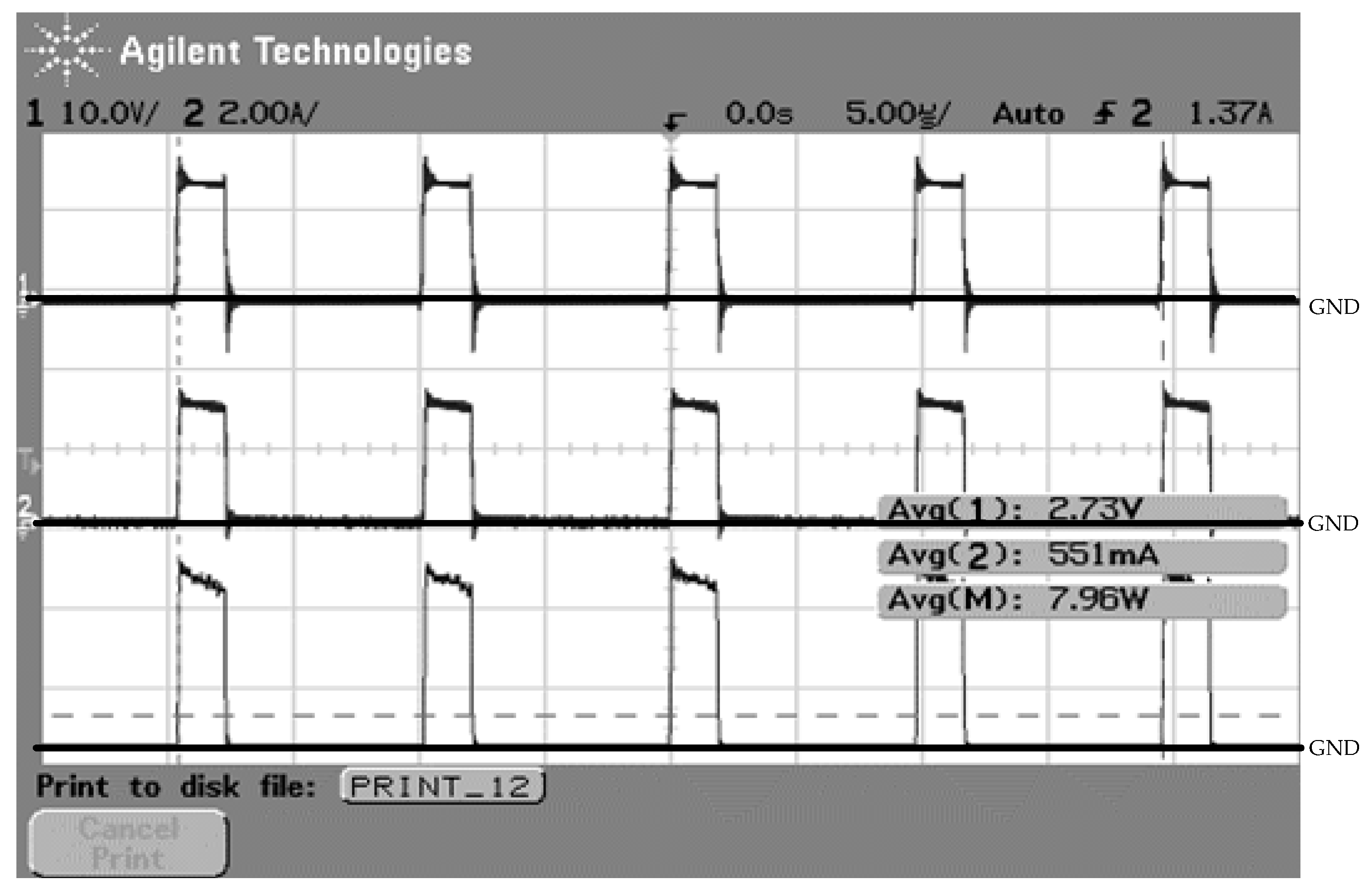
Experimental results are presented in Figure 17, Figure 18, Figure 19 and Figure 20. To confirm the operation of the simplified boost converter with a reduced number of components, a simplified booster converter was used. The components used are: L = 70 µH, transistor = IRF540, LED = 3 W LED with 6 in series. The circuit as shown in Figure 8 was used for the test. The brightness of the LEDs could be regulated successfully by the duty ratio control, as shown in Appendix A. Figure 17 shows experimental waveforms of the boost converter at switching frequency fs = 50 kHz and 80% duty ratio. Figure 18 shows the output waveforms, with the output voltage impressed onto the LED. The measured efficiency was 69%. From Section 2.4.2, we know that the efficiency of circuits with ideal elements was close to 1. The error was 31%. The reason was the switching losses of the LEDs and the transistor. Figure 19 and Figure 20 show the results at 100 kHz with 80% duty ratio. The dimming could be regulated successfully. The LED illumination output was confirmed to be regulated successfully by the high-frequency switching signal.
5. Discussion
When compared with the classical LED driving topologies presented in [13,14,15,16,17,18], the proposed new family of power converters have the following advantages: First, the design can be used to reduce the cost and components. Since the LEDs are put in the diode, transistor, and inducer paths, the drivers can have less components. Thus, if a small size is required, the corresponding size can be reduced. Second, the proposed converters can work at low voltage. Third, high efficiency is achieved without a complicated control circuit. In Figure 11, Figure 12 and Figure 13, the proposed power converters could achieve high efficiency at specific duty ratios. However, current high efficiency research often focuses on high LED power applications [36]. These new power converters can be used in special occasions where low voltage, low size, and high efficiency is needed. Moreover, the output ripple amplitude is low in this family of power converters. From theoretical analyses, the output voltage ripple of the proposed LED drivers can be reduced significantly at specific duty ratios.
However, this paper pays more attention to the topology and theoretical derivation. All the circuit components are ideal in this paper. Therefore, in some cases, the efficiency can be close to 100%. But for real circuits, there are switching losses and conduction losses of LEDs and the transistor.
The switching losses of MOSFET PSW in this paper can be expressed as [37]:
where Idmax is the maximum current through MOSFET, and tcross is overlap time.
The conduction losses of MOSFET PCOND in this paper can be expressed as [37]:
where IRMS is the root–mean–square value of the current, and Rds is resistance.
When the efficiency is being calculated, PSW and PCOND should be taken into account.
LED is the freewheeling diode in Section 2.2 and Section 2.4. The conduction losses of the freewheeling diode cannot be neglected. The conduction losses of freewheeling diode PCOND-D are:
where ID_AVG is the diode average current.
The way to reduce the conduction losses is to reduce the forward voltage drop of the diode and the transistor.
The switching losses of the freewheeling diode or LED include turn-on losses and turn-off losses.
Turn-on losses can be derived as:
where tfp is the forward recovery time, Vfp is the peak forward voltage, and Ifp is the peak forward current.
Turn-on losses are:
where trp is the reverse current descent time, Vrp is the peak back voltage, and Irp is the peak back current.
When the efficiency is calculated, PSW, PCOND, PCOND-D, PD,turn-off, and PD,turn-on should be taken into account. In the next research, we will build circuits to verify these topologies, and the ideal elements will be replaced by real ones.
There is another issue that should be taken into account. Because uneven voltage is inevitable among the LEDs, this factor can affect the life of LEDs, which leads to potential safety problems for the circuits. As the LED lifespan increases, the driver controls the overall lifetime of the LED system. However, the driver consists of a number of components, and the components’ lifespan is usually less than that of LED chips; therefore, the safety issue is still unknown. The authors will explore these issues in our next research.
6. Conclusions
In this paper, we propose a new family of power converters to the low-power LED lighting for lighting and special effect design. It was found that the LED could replace the freewheel diode in the converters. It can also be placed in the transistor and inducer paths. The proposed circuits reduce both the cost and component count through simplifying the classic driving for LEDs, especially for LEDs in inductor path circuits. The formulation of an output conversion ratio, power of the LED, and the efficiency was derived. Efficiency and output ripple amplitude of the proposed circuit topologies are discussed in this paper. Analytical study shows that efficiency of proposed circuits can be high. Buck, buck–boost, and Ćuk LEDs in transistor path circuits have relatively high efficiency. It should be emphasized that buck and boost LEDs in diode path circuits and all LEDs in inductor path circuits have almost no loss. It was found that low output ripple amplitude could be obtained for the proposed circuits. For buck and buck–boost LEDs in transistor path circuits, voltage ripple magnitude was very low (ΔVLED/nVLED < 0.4% for buck, ΔVLED/nVLED < 1.6% for buck–boost). The results also show that the proposed circuit topologies could be easily adopted to design LED lighting because high efficiency, less components, and low voltage ripple magnitude criteria can be met at the same time. Finally, the experimental waveforms of the laboratory prototype confirmed the operation of the simplified converter.
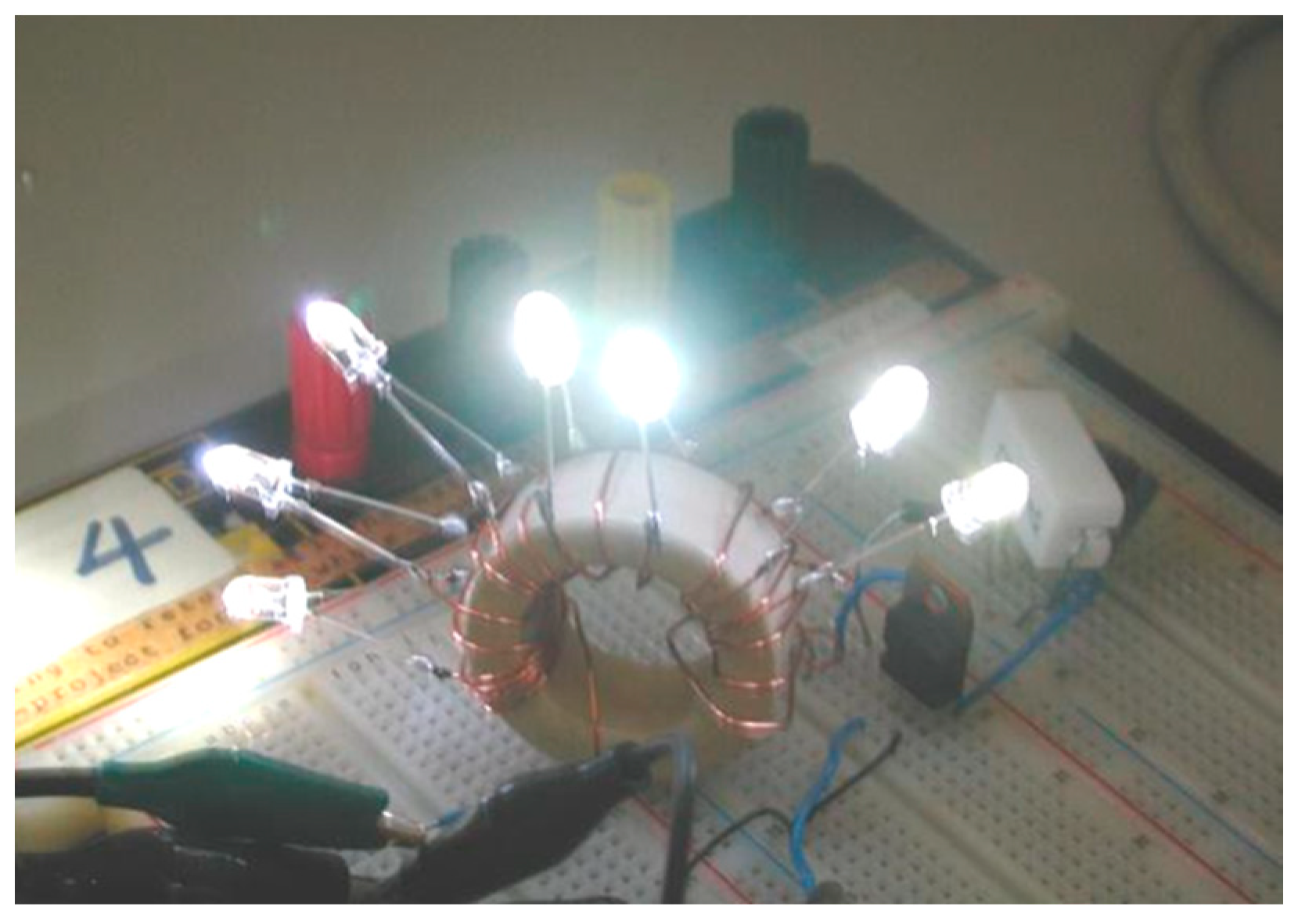
An LED integrated in the inductor winding has been demonstrated that is another method of integration of inductor and LEDs by combining the LED leads and inductor winding. It is shown in Appendix A.
Author Contributions
Conceptualization, W.C., K.W.E.C., and J.S.; investigation, W.C. and K.W.E.C.; writing—review and editing, W.C. and K.W.E.C.; supervision, K.W.E.C.
Funding
This research was funded by the Research Committee of the Hong Kong Polytechnic University under the project code: 845G and ZDBL.
Conflicts of Interest
The authors declare no conflict of interest.
Appendix A
Figure A1.
The LED connected in inductor path.
References
- Li, S.; Tan, S.; Lee, C.K.; Waffenschmidt, E.; Hui, S.Y.; Tse, C.K. A survey, classification, and critical review of light-emitting diode drivers. IEEE Trans. Power Electron. 2016, 31, 1503–1516. [Google Scholar] [CrossRef]
- Lin, H.; Hu, J.; Zhou, X.; Lu, Z.; Wang, L. New DC Grid Power Line Communication Technology Used in Networked LED Driver. Energies 2018, 11, 3531. [Google Scholar] [CrossRef]
- Arias, M.; Lamar, D.G.; Sebastian, J.; Balocco, D.; Diallo, A.A. High-Efficiency LED Driver Without Electrolytic Capacitor for Street Lighting. IEEE Trans. Ind. Electron. 2013, 49, 127–137. [Google Scholar] [CrossRef]
- Liu, Y.-C.; Chen, C.; Chen, K.-D.; Syu, Y.-L.; Tsai, M.-C. High-Frequency LLC Resonant Converter with GaN Devices and Integrated Magnetics. Energies 2019, 12, 1781. [Google Scholar] [CrossRef]
- Cheng, K.W.E.; Wang, H.; Cheng, D.K.W. Derivation of an Electronic Ballast with a Secondary DC Output. Int. J. Circ. Theor. Appl. 2007, 14, 466. [Google Scholar]
- Yan, W.; Hui, S.Y. An analysis into the dimming control and characteristic of discharge lamps. IEEE Trans. Power Electron. 2005, 20, 1432–1440. [Google Scholar] [CrossRef]
- Dong, P.; Cheng, K.W.E.; Wang, D.H.; Divakar, B.P. Investigation on the Modeling and Ageing Characteristics of the HID Car Headlight Automotive System. J. Key Eng. Mater 2008, 364, 1280–1284. [Google Scholar]
- European Commission. Low Voltage Directive 2006/95/EC; The European Parliament and of The Council, Official Journal of the European Union: Brussels, Belgium, 2006. [Google Scholar]
- Choi, W.Y.; Kwon, J.M.; Kwon, B.H. Efficient LED back-light power supply for liquid-crystal-display. IET Electr. Power Appl. 2007, 1, 133–142. [Google Scholar] [CrossRef]
- Lo, Y.; Wu, K.; Pai, K.; Chiu, H. Design and Implementation of RGB LED Drivers for LCD Backlight Modules. IEEE Trans. Ind. Electron. 2009, 56, 4862–4871. [Google Scholar]
- Cheng, K.W.E. Classical Switched Mode and Resonant Power Converter; The Hong Kong Polytechnic University: Hong Kong, China, 2002; Chapter 2; pp. 15–64. ISBN 962-367-364-7. [Google Scholar]
- Hui, S.Y.; Li, S.N.; Tao, X.H.; Chen, W.; Ng, W.M. A Novel Passive Offline LED Driver with Long Lifetime. IEEE Trans. Power Electron. 2010, 25, 2665–2672. [Google Scholar] [CrossRef]
- Baek, J.; Chae, S. Single-Stage Buck-Derived LED Driver with Improved Efficiency and Power Factor Using Current Path Control Switches. IEEE Trans. Ind. Electron. 2017, 64, 7852–7861. [Google Scholar] [CrossRef]
- Lu, Y.; Czarkowski, D.; Bury, W.E. High efficiency adaptive boost converter for LED drivers. In Proceedings of the 2011 7th International Conference-Workshop Compatibility and Power Electronics (CPE), Tallinn, Estonia, 1–3 June 2011; pp. 315–318. [Google Scholar]
- Mannam, R.; Vangala, N. Soft switching boost converter for DC input LED drivers. In Proceedings of the 2016 7th India International Conference on Power Electronics (IICPE), Patiala, India, 17–19 November 2016; pp. 1–5. [Google Scholar]
- Lin, R.; Chang, Y.; Lee, C. Optimal Design of LED Array for Single-Loop CCM Buck–Boost LED Driver. IEEE Trans. Ind. Electron. 2013, 49, 761–768. [Google Scholar] [CrossRef]
- Mohamed, L.; Hamid, N.F.A.; Isa, Z.M.; Saudin, N.; Ramly, N.H.; Ahamad, N.B. Cuk converter as a LED lamp driver. In Proceedings of the 2012 IEEE International Conference on Power and Energy (PECon), Kota Kinabalu, Malaysia, 2–5 December 2012; pp. 262–267. [Google Scholar]
- Lin, W.; Yuzhen, X.; Zheng, Q.L. A high efficiency integrated step-down Cuk and flyback converter for LED power driver. In Proceedings of the 2015 9th International Conference on Power Electronics and ECCE Asia (ICPE-ECCE Asia), Seoul, Korea, 1–5 June 2015; pp. 60–64. [Google Scholar]
- Chan, H.L.; Cheng, K.W.E.; Sutanto, D. Phase-shift controlled DC-DC converter with bi-directional power flow. IEE Proc.-Electr. Power Appl. 2001, 148, 193–201. [Google Scholar] [CrossRef]
- Lun, W.; Loo, K.H.; Tan, S.; Lai, Y.M.; Tse, C.K. Bilevel Current Driving Technique for LEDs. IEEE Trans. Power Electron 2009, 24, 2920–2932. [Google Scholar]
- Chen, H.; Tan, S.; Hui, S.Y. Color Variation Reduction of GaN-Based White Light-Emitting Diodes Via Peak-Wavelength Stabilization. IEEE Trans. Power Electron. 2014, 29, 3709–3719. [Google Scholar] [CrossRef]
- Cheng, K.W.E. Storage energy for classical switched mode power converters. IEE Proc.-Electr. Power Appl. 2003, 150, 439–446. [Google Scholar] [CrossRef]
- Jang, Y.; Jovanović, M.M. Bridgeless high-power-factor buck converter. IEEE Trans. Power Electron. 2011, 26, 602–611. [Google Scholar] [CrossRef]
- Cheng, H.; Lin, C. Design and Implementation of a High-Power-Factor LED Driver with Zero-Voltage Switching-On Characteristics. IEEE Trans. Power Electron. 2014, 29, 4949–4958. [Google Scholar] [CrossRef]
- Wu, X.; Xie, X.; Chen, Z.; Qian, Z.; Zhao, R. Low voltage and current stress ZVZCS full bridge DC–DC converter using center tapped rectifier reset. IEEE Trans. Ind. Electron. 2008, 55, 1470–1477. [Google Scholar] [CrossRef]
- Hsieh, H.I.; Li, J.S.; Chen, D. Effects of X capacitors on EMI filter effectiveness. IEEE Trans. Ind. Electron. 2008, 55, 949–955. [Google Scholar] [CrossRef]
- Narendran, N.; Gu, Y. Life of LED-based white light sources. IEEE Disp. Technol. 2005, 1, 167. [Google Scholar] [CrossRef]
- Hsieh, Y.Y.; Juang, Y.Z. Analysis and suppression of overcurrent in boost LED drivers. IEEE Disp. Technol. 2013, 9, 388–395. [Google Scholar] [CrossRef]
- Dong, Z.; Tse, C.K.; Hui, S.Y.R. Circuit Theoretic Considerations of LED Driving: Voltage-Source Versus Current-Source Driving. IEEE Trans. Power Electron. 2019, 34, 4689–4702. [Google Scholar] [CrossRef]
- Saini, D.K.; Ayachit, A.; Salvatierra, T.; Kazimierczuk, M.K. Design of zero-voltage-ripple buck dc-dc converter. In Proceedings of the 2017 IEEE 60th International Midwest Symposium on Circuits and Systems (MWSCAS), Boston, MA, USA, 6–9 August 2017; pp. 456–459. [Google Scholar]
- Reddy, U.R.; Narasimharaju, B.L. Single-stage electrolytic capacitor less non-inverting buck-boost PFC based AC–DC ripple free LED driver. IET Power Electron. 2017, 10, 38–46. [Google Scholar] [CrossRef]
- Yu, Y.; Zhang, F.; Ni, J. Capacitor clamped current sharing circuit for multistring LEDs. In Proceedings of the 2012 IEEE Energy Conversion Congress and Exposition (ECCE), Raleigh, NC, USA, 15–20 September 2012; pp. 3568–3574. [Google Scholar]
- Hwu, K.; Jiang, W. Input-Current-Ripple-Free Two-Channel LED Driver. IEEE Trans. Ind. Electron. 2017, 64, 5865–5874. [Google Scholar] [CrossRef]
- Wu, X.K.; Zhang, J.M.; Zhao, M.Q. A simple two-channel LED driver with automatic precise current sharing. IEEE Trans. Ind. Electron. 2011, 58, 4783–4788. [Google Scholar] [CrossRef]
- Zhao, C.; Xie, X.; Liu, S. Multioutput LED drivers with precise passive current balancing. IEEE Trans. Power Electron. 2013, 28, 1438–1448. [Google Scholar] [CrossRef]
- Lee, E.S.; Choi, B.H.; Nguyen, D.T.; Choi, B.G.; Rim, C.T. Static regulated multistage semiactive LED drivers for high-efficiency applications. IEEE Trans. Power Electron. 2015, 31, 6543–6552. [Google Scholar] [CrossRef]
- Maniktala, S. Switching Power Supplies A–Z; Elsevier: Amsterdam, The Netherlands, 2012. [Google Scholar]
Figure 1.
Conventional method for LED connection. (a) Basic LED buck converter; (b) Basic LED boost converter; (c) Basic LED buck–boost converter; (d) Basic LED Ćuk converter.
Figure 1.
Conventional method for LED connection. (a) Basic LED buck converter; (b) Basic LED boost converter; (c) Basic LED buck–boost converter; (d) Basic LED Ćuk converter.
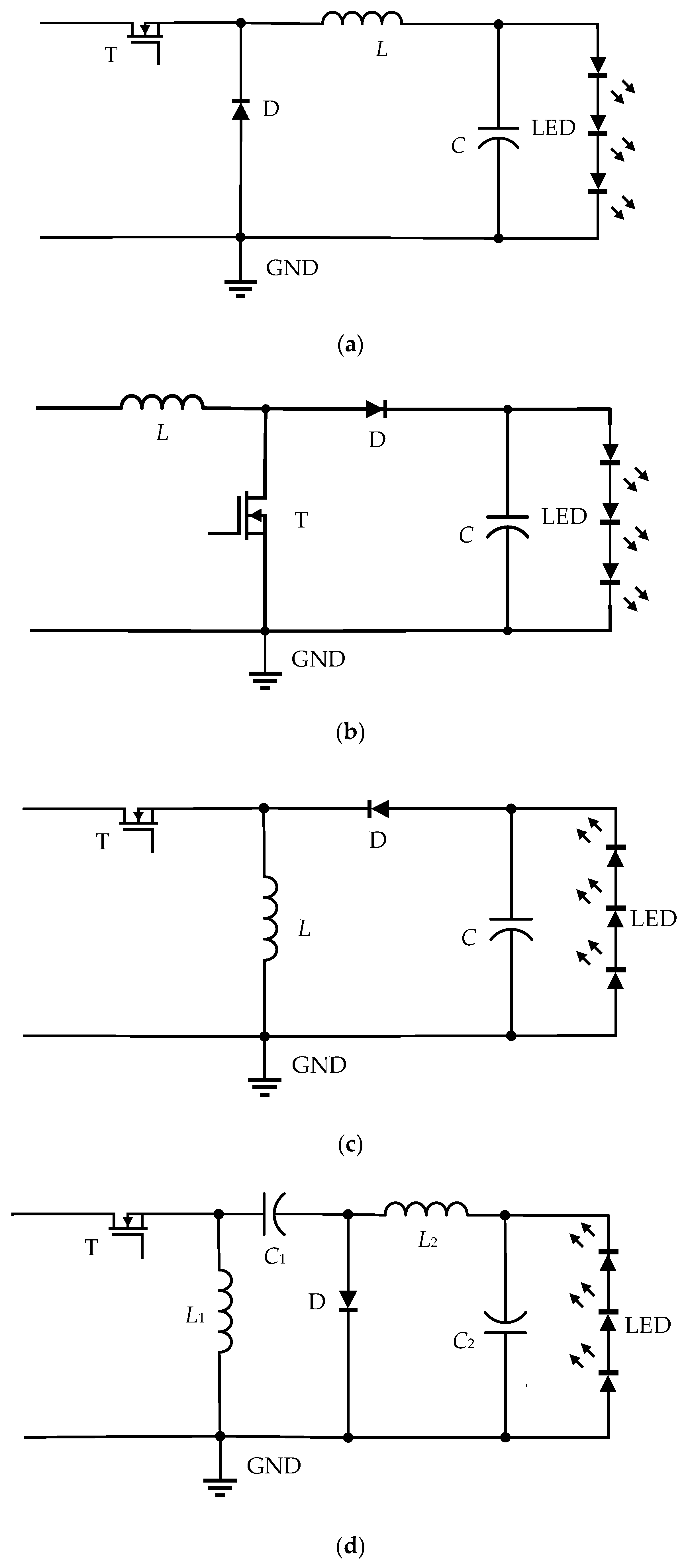
Figure 2.
LED buck converter.
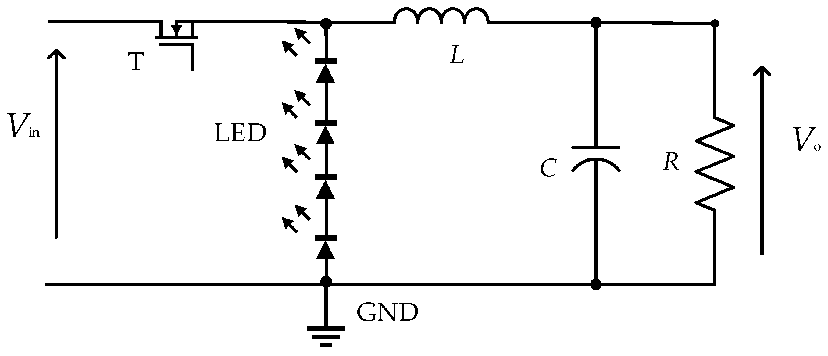
Figure 3.
LED Boost converter.

Figure 4.
LED buck–boost converter.
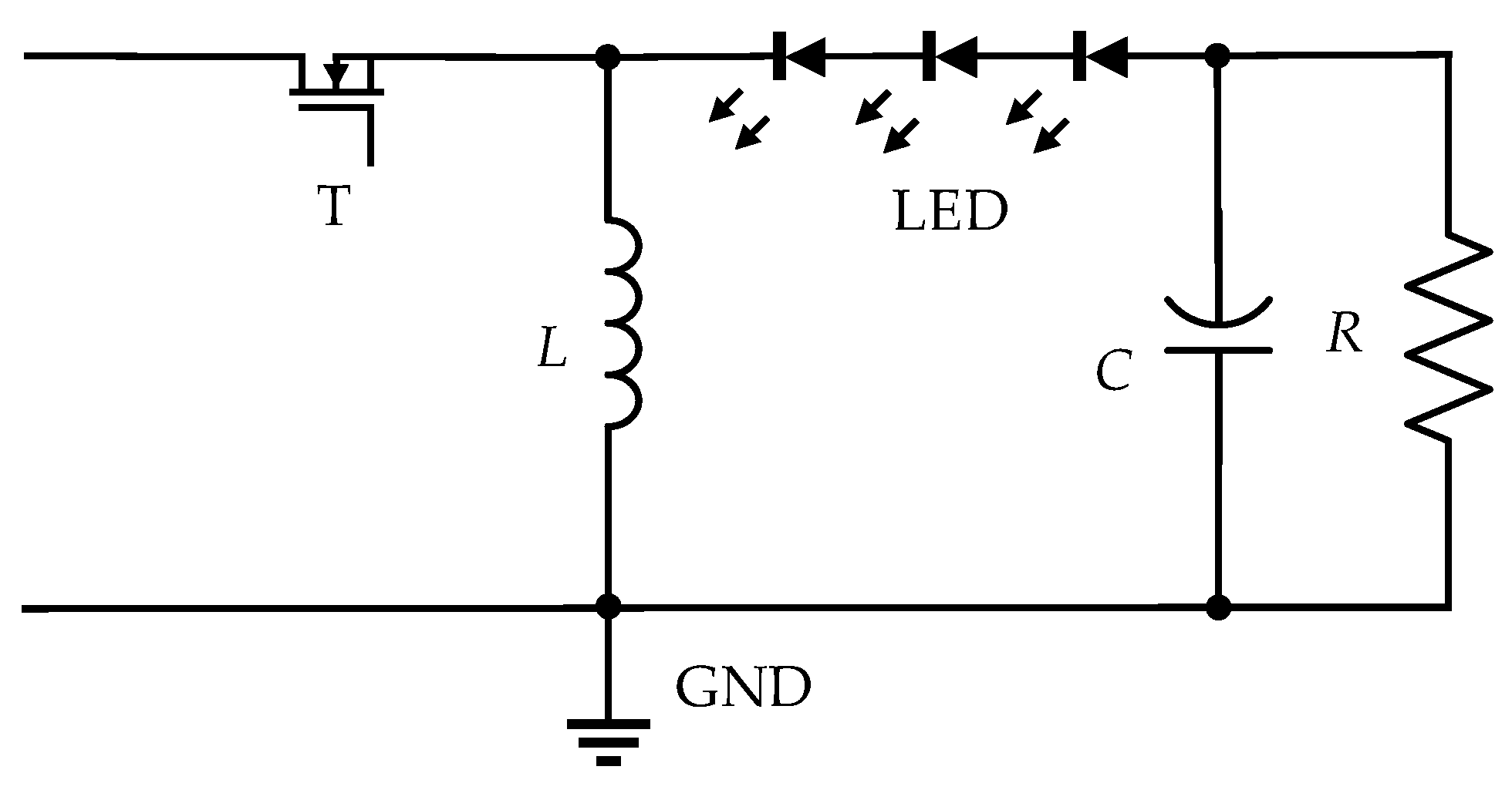
Figure 5.
LED Ćuk converter.
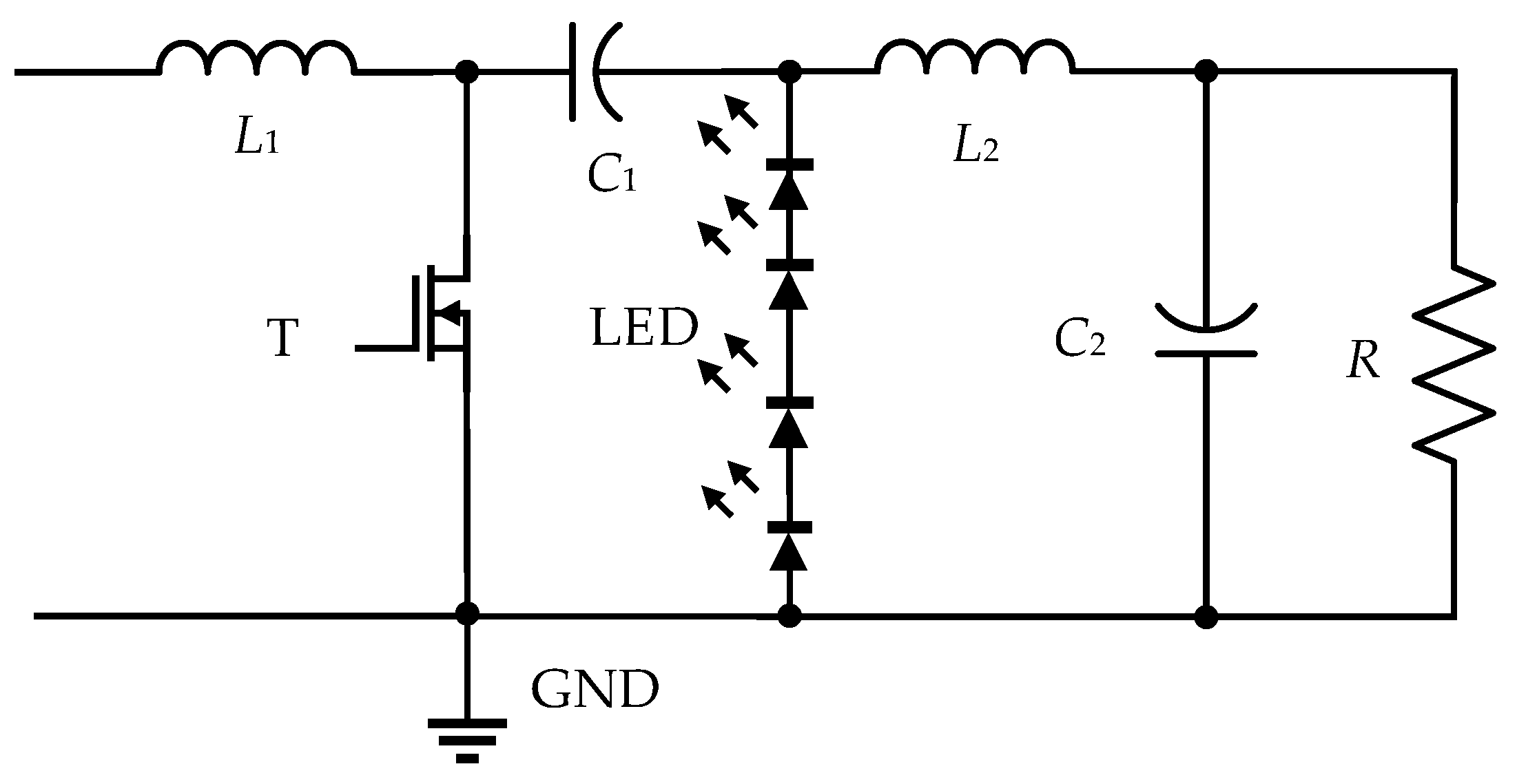
Figure 6.
Transistor path LED converter. (a) Buck; (b) Boost; (c) Buck–Boost; (d) Ćuk.
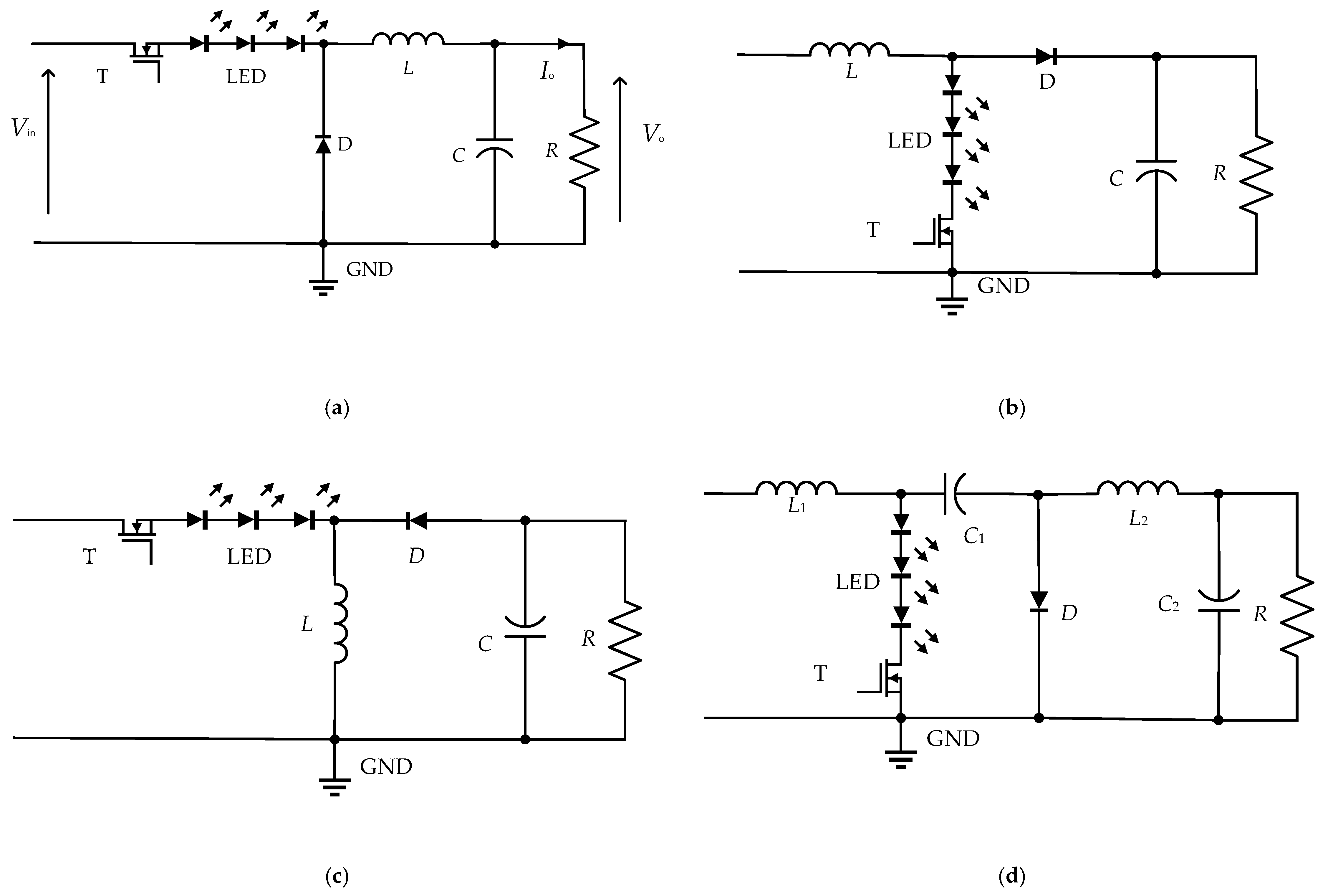
Figure 7.
Simplified LED chopper like a “buck” converter.

Figure 8.
Simplified LED Boost converter.
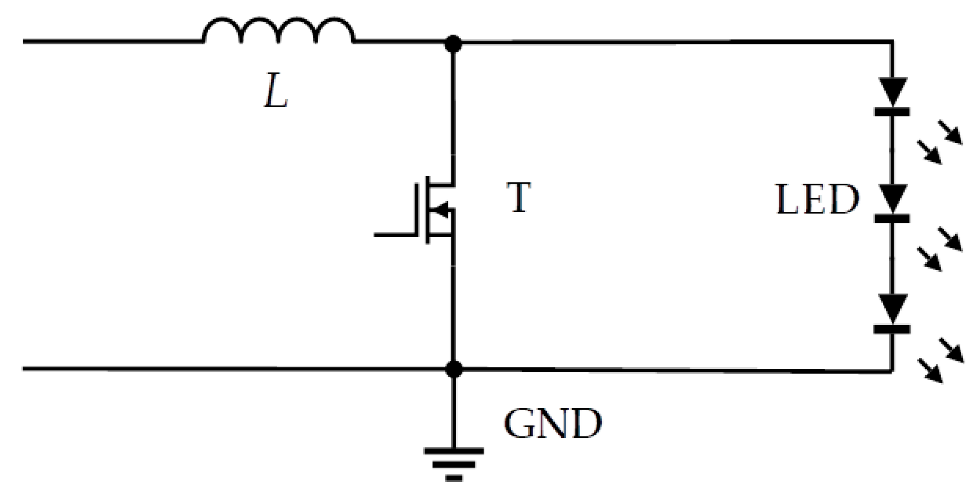
Figure 9.
Simplified LED buck–boost converter.
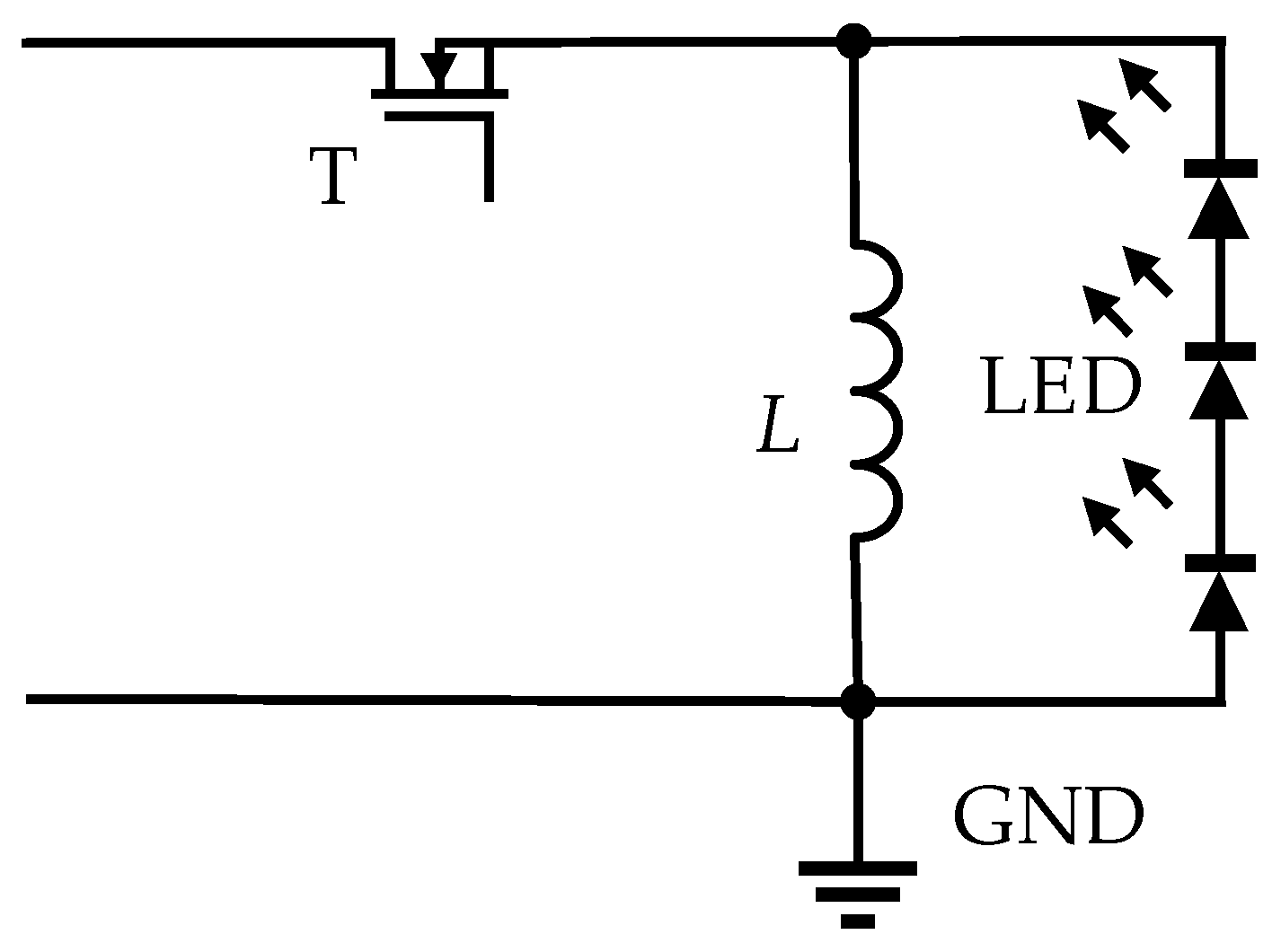
Figure 10.
Simplified LED Ćuk converter.

Figure 11.
Relationship between efficiency and D of the LED in the diode converter.
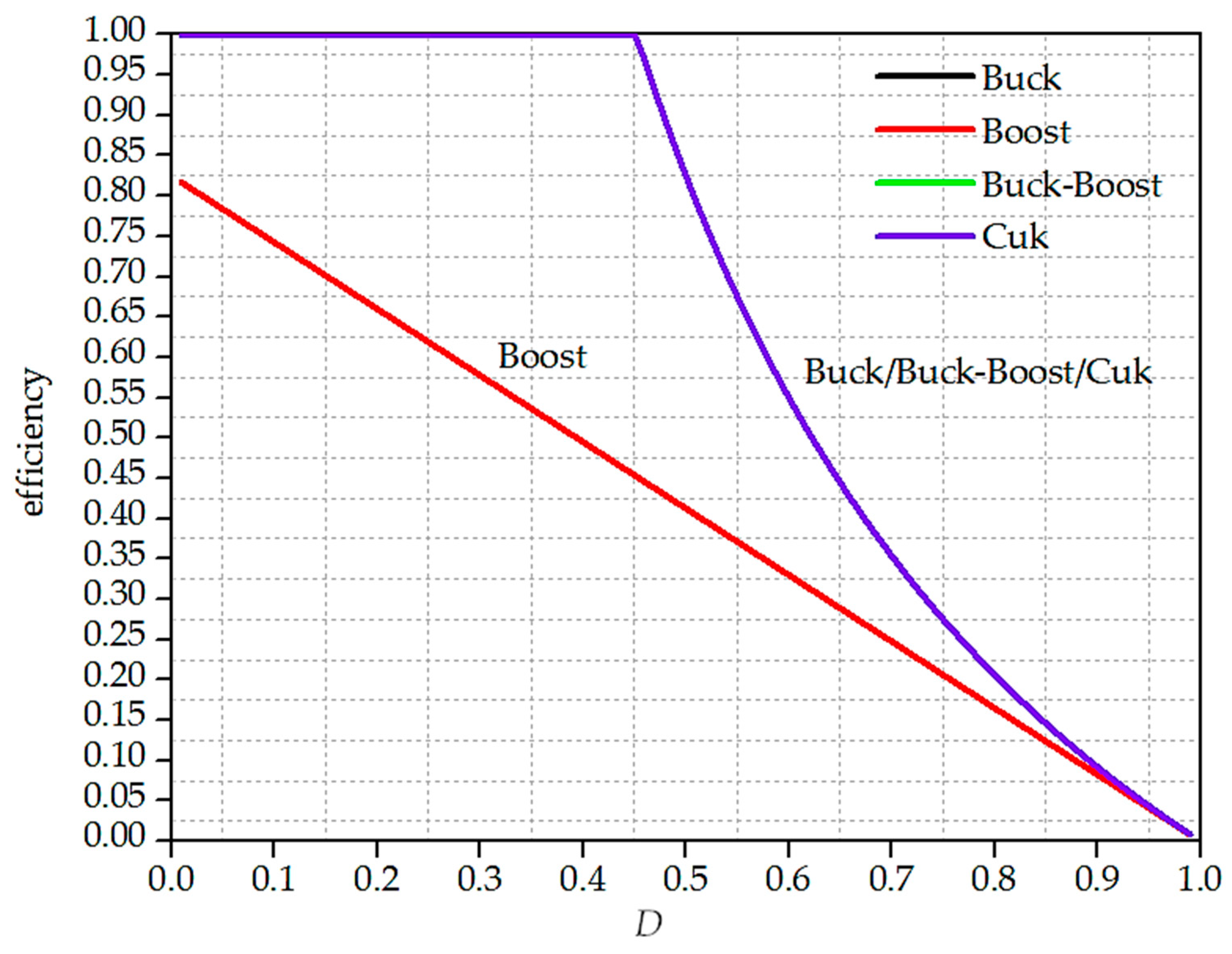
Figure 12.
Relationship between efficiency and D of the LED in transistor converter.
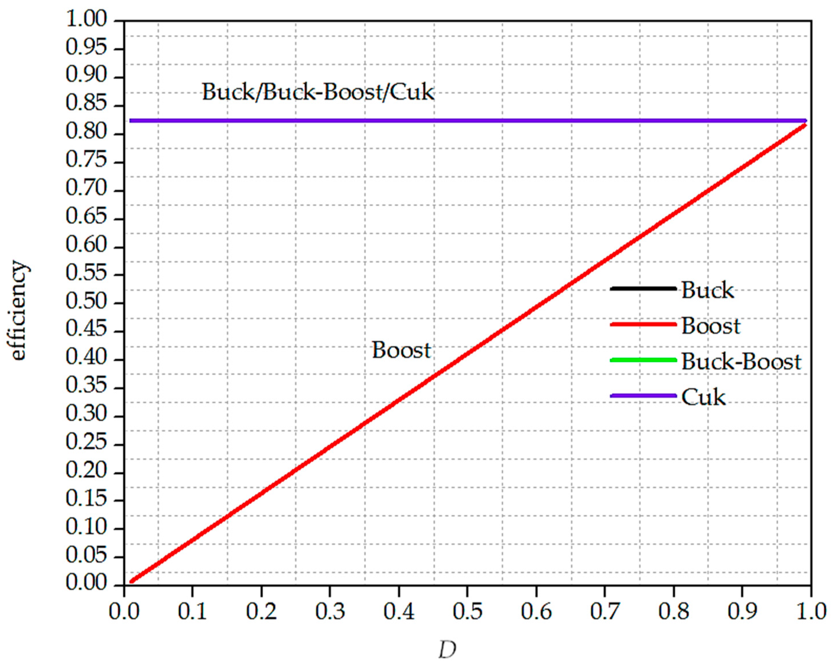
Figure 13.
Relationship between efficiency and D of the LED in inductor converter.
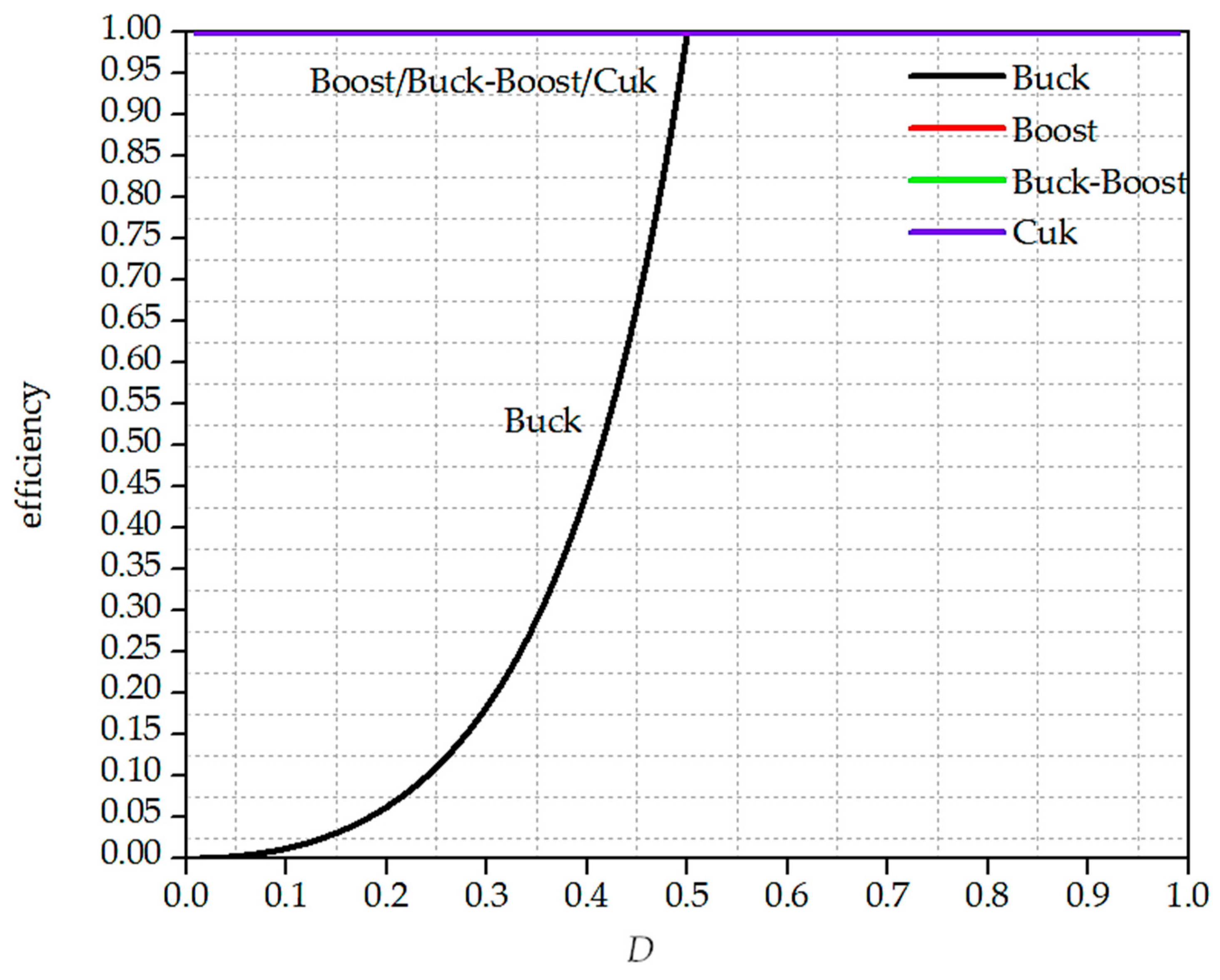
Figure 14.
Relationship between voltage ripple magnitude and D of the LED in diode converters.
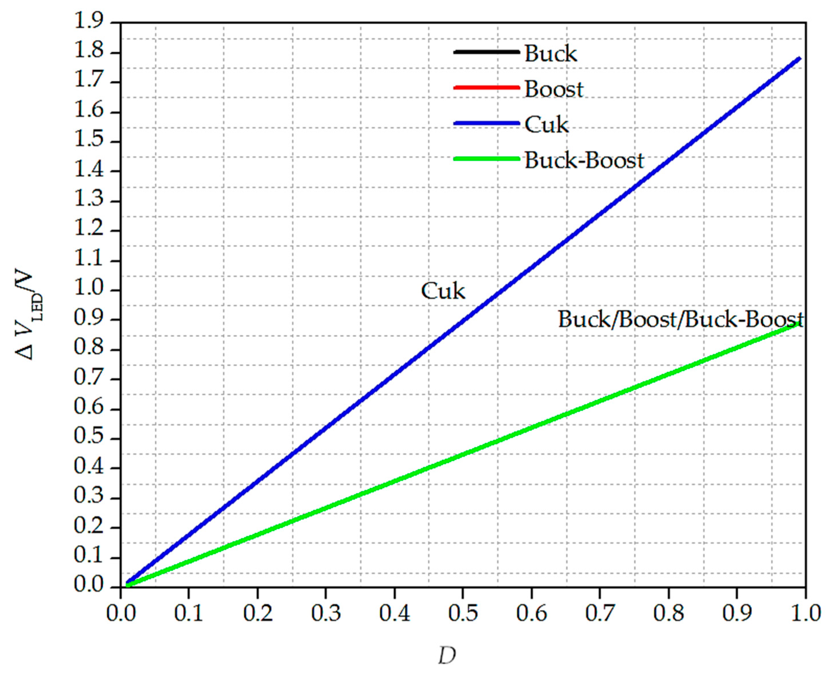
Figure 15.
Relationship between voltage ripple magnitude and D of the LED in transistor converters.
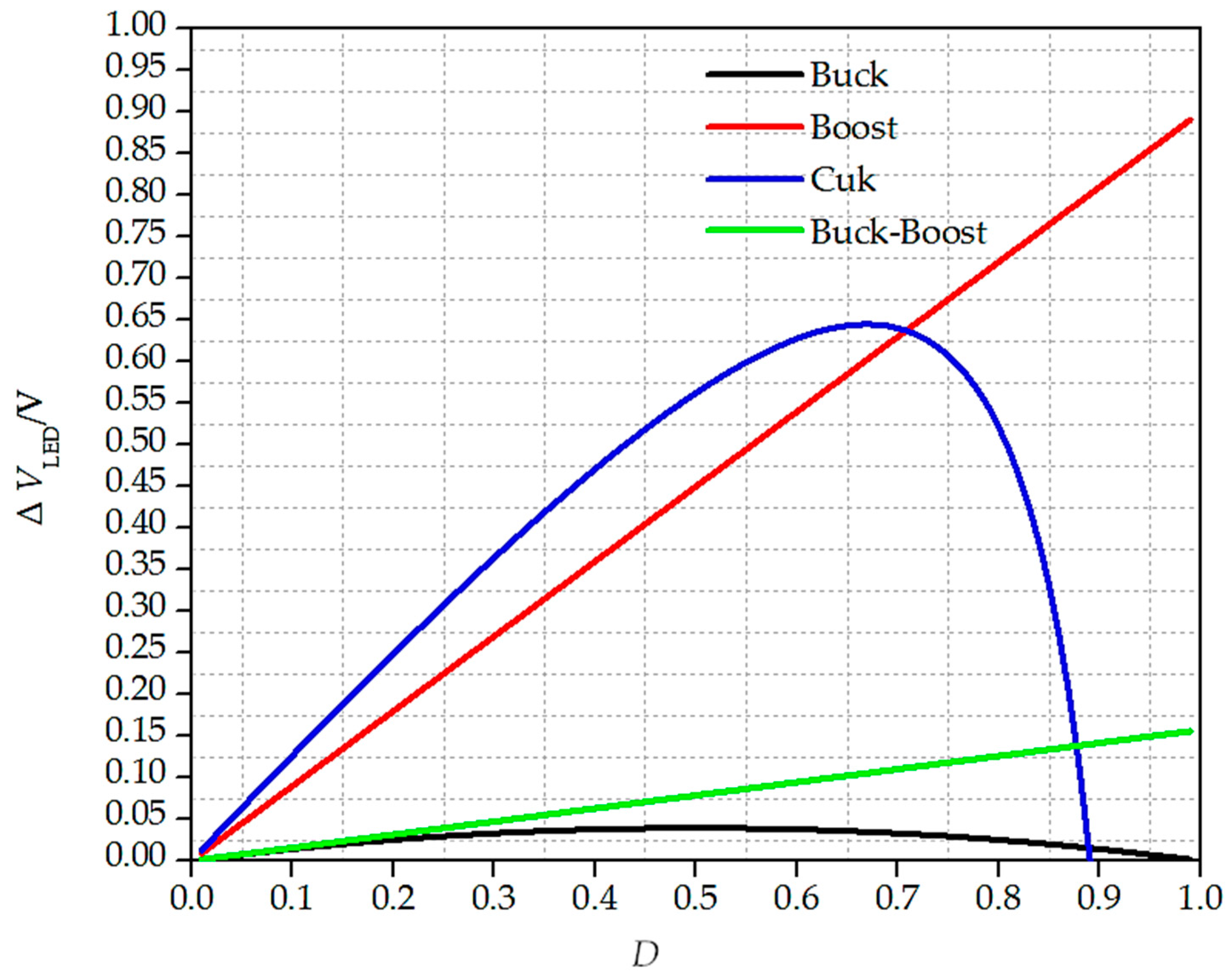
Figure 16.
Relationship between voltage ripple magnitude and D of the LED in inductor converters.
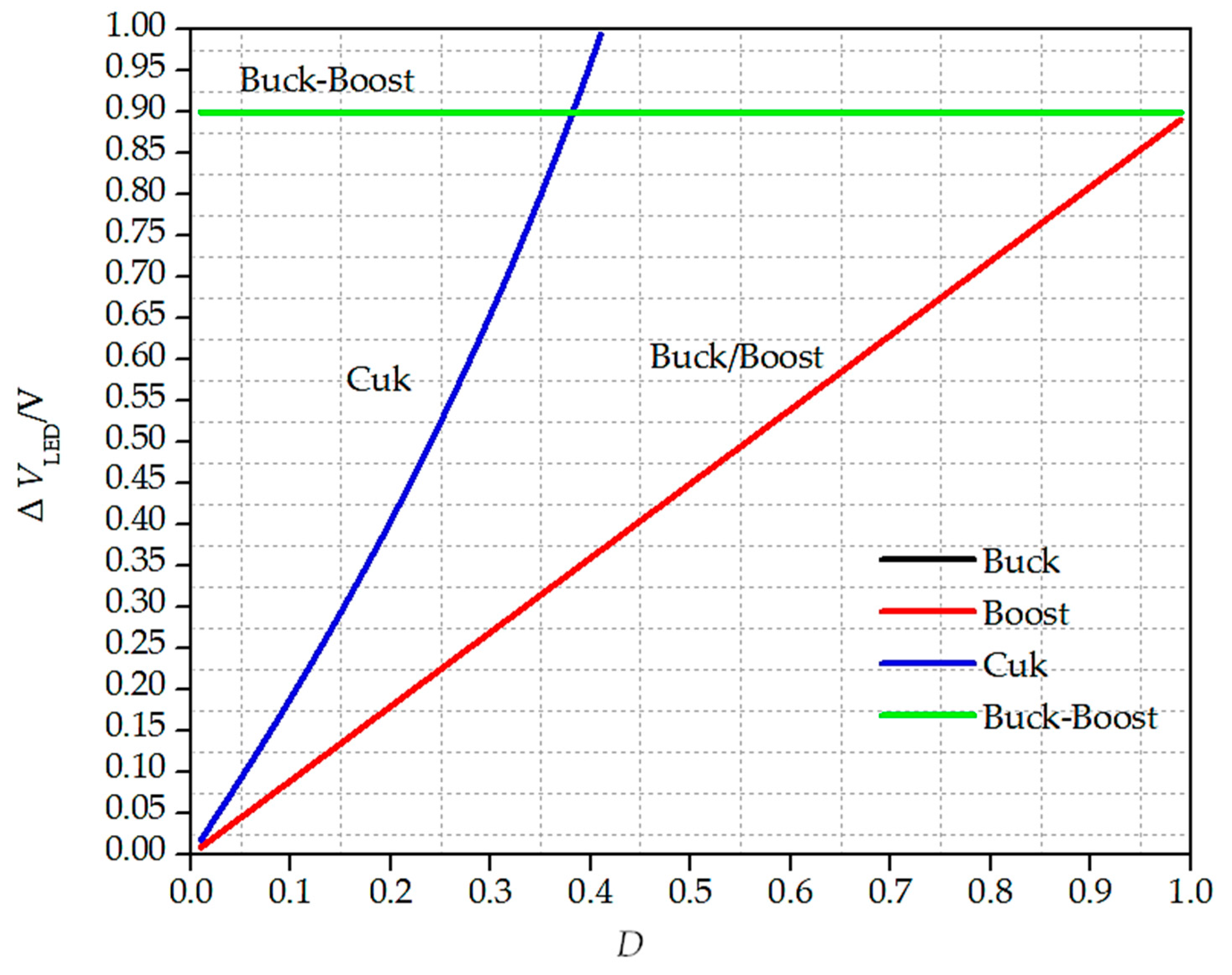
Figure 17.
Input characteristics of the proposed boost converter with fs = 50 kHz. (Top Trace) Input Voltage (5 V/div); (Middle Trace) Input Current (2 A/div); (Bottom Trace) Input Power (2 W/div).
Figure 17.
Input characteristics of the proposed boost converter with fs = 50 kHz. (Top Trace) Input Voltage (5 V/div); (Middle Trace) Input Current (2 A/div); (Bottom Trace) Input Power (2 W/div).
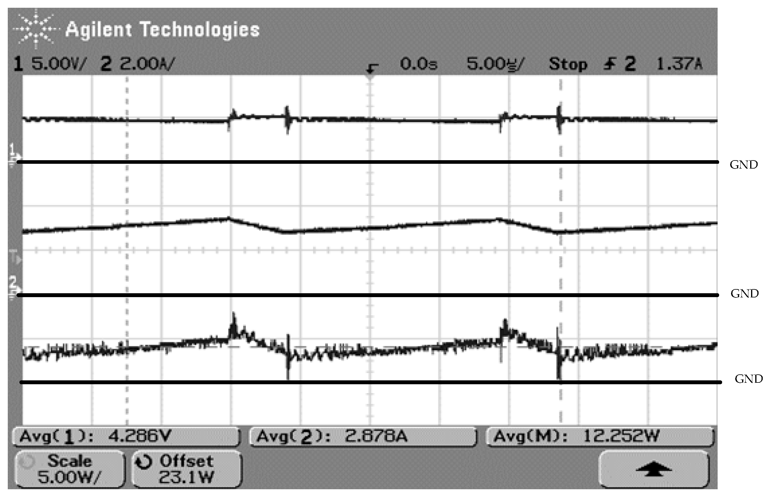
Figure 18.
Output characteristics of proposed boost converter with fs = 50 kHz. (Top Trace) Output Voltage (10 V); (Middle Trace) Output Current (2 A/div); (Bottom Trace) Output Power (20 W/div).
Figure 18.
Output characteristics of proposed boost converter with fs = 50 kHz. (Top Trace) Output Voltage (10 V); (Middle Trace) Output Current (2 A/div); (Bottom Trace) Output Power (20 W/div).
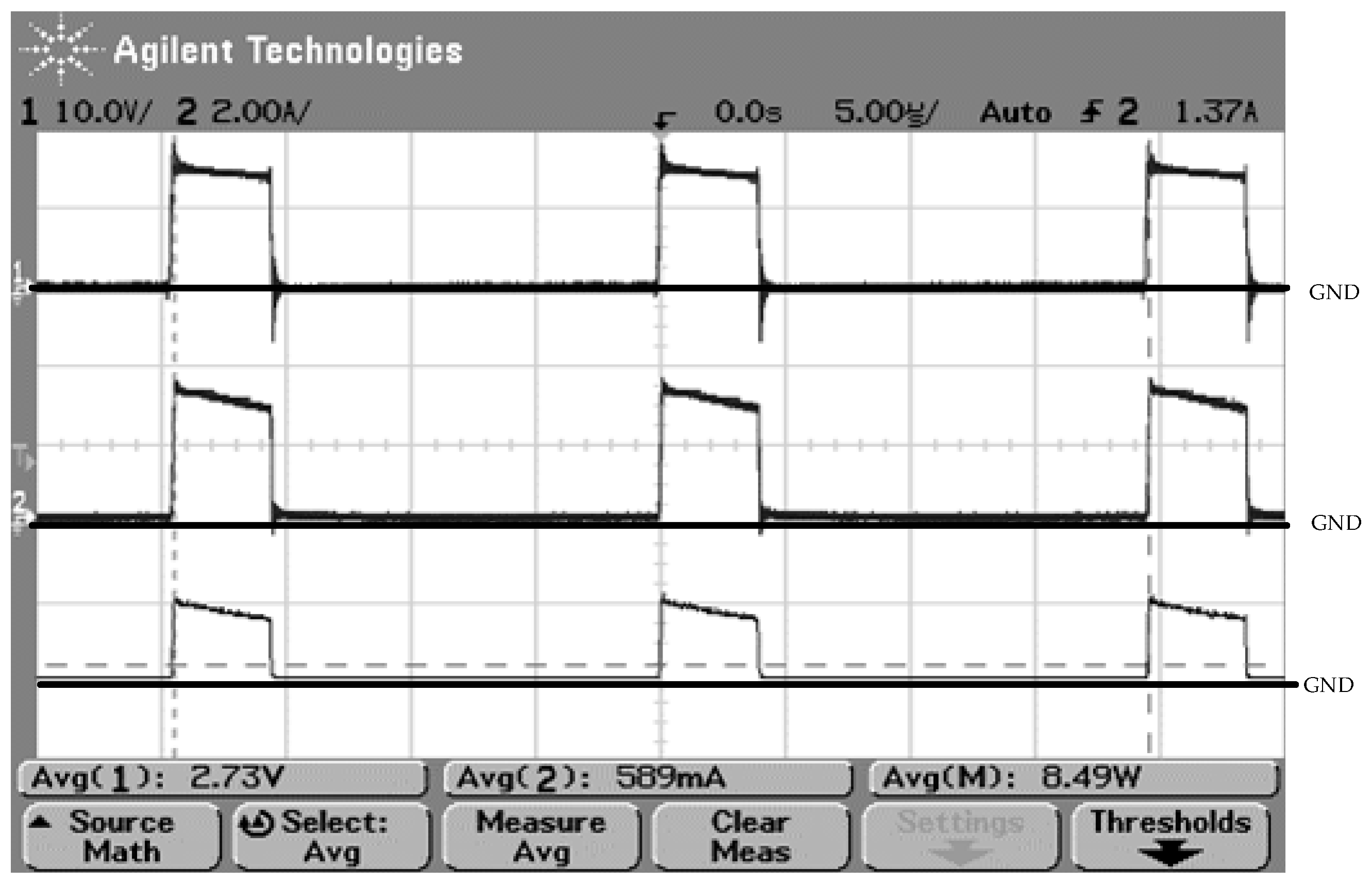
Figure 19.
Input characteristics of the proposed boost converter with fs = 100 kHz. (Top Trace) Input Voltage; (Middle Trace) Input Current; (Bottom Trace) Input Power.
Figure 19.
Input characteristics of the proposed boost converter with fs = 100 kHz. (Top Trace) Input Voltage; (Middle Trace) Input Current; (Bottom Trace) Input Power.
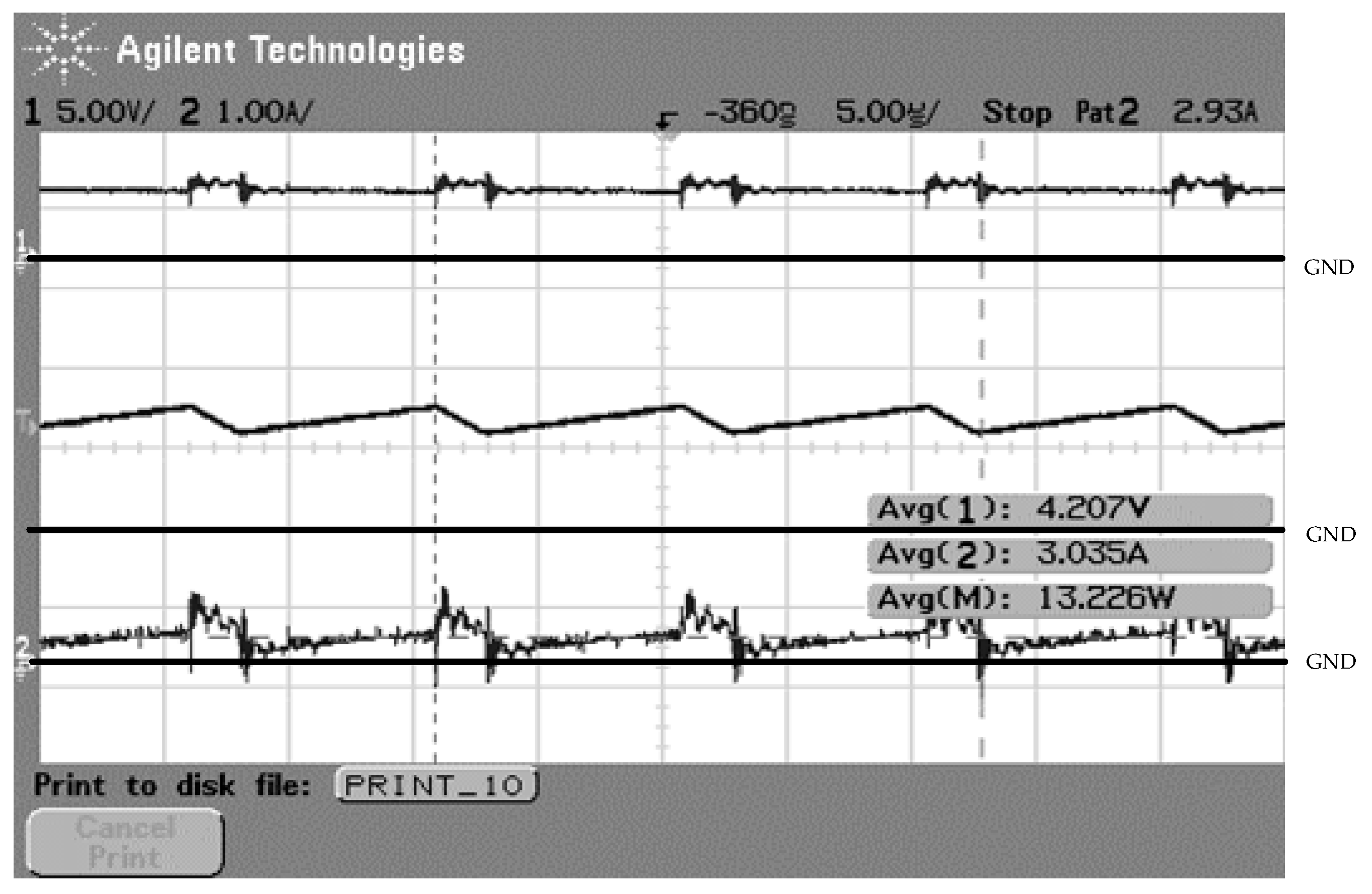
Figure 20.
Output characteristics of proposed boost converter with fs = 100 kHz. (Top Trace) Output Voltage; (Middle Trace) Output Current; (Bottom Trace) Output Power.
Figure 20.
Output characteristics of proposed boost converter with fs = 100 kHz. (Top Trace) Output Voltage; (Middle Trace) Output Current; (Bottom Trace) Output Power.

Table 1.
Output efficiency of different LEDs’ driving circuit topologies.
| Topology | LED in the Diode Path | LED in the Transistor Path | LED in the Inductor Path |
|---|---|---|---|
| Buck | |||
| Boost | close to 1 | ||
| Buck–Boost | close to 1 | ||
| Ćuk | close to 1 |
Table 2.
Output voltage ripples of different LEDs’ driving circuit topologies.
| Topology | LED in the Diode Path | LED in the Transistor Path | LED In The Inductor Path |
|---|---|---|---|
| Buck | |||
| Boost | |||
| Buck–Boost | |||
| Ćuk |
© 2019 by the authors. Licensee MDPI, Basel, Switzerland. This article is an open access article distributed under the terms and conditions of the Creative Commons Attribution (CC BY) license (http://creativecommons.org/licenses/by/4.0/).
Share and Cite
MDPI and ACS Style
Chen, W.; Cheng, K.W.E.; Shao, J. Circuit Topology Analysis for LED Lighting and its Formulation Development. Energies 2019, 12, 4203. https://doi.org/10.3390/en12214203
AMA Style
Chen W, Cheng KWE, Shao J. Circuit Topology Analysis for LED Lighting and its Formulation Development. Energies. 2019; 12(21):4203. https://doi.org/10.3390/en12214203
Chicago/Turabian StyleChen, William, Ka Wai Eric Cheng, and Jianwei Shao. 2019. "Circuit Topology Analysis for LED Lighting and its Formulation Development" Energies 12, no. 21: 4203. https://doi.org/10.3390/en12214203
Note that from the first issue of 2016, this journal uses article numbers instead of page numbers. See further details here.