Double-Layer E-Structure Equalization Circuit for Series Connected Battery Strings

School of Electrical Engineering, Southwest Jiaotong University, Chengdu 611756, China
*
Author to whom correspondence should be addressed.
Energies 2019, 12(22), 4252; https://doi.org/10.3390/en12224252
Submission received: 10 October 2019
/
Revised: 1 November 2019
/
Accepted: 5 November 2019
/
Published: 8 November 2019
(This article belongs to the Special Issue Testing and Management of Lithium-Ion Batteries)
Abstract
:In order to eliminate the voltage imbalance among battery cells when they are connected in series, the paper proposes a double-layer E-structure (DLE) equalizer based on bidirectional buck–boost converters, which has the advantage of quick equalization speed and can be applied to arbitrary number batteries. Furthermore, a novel two-stage equalization control strategy is proposed for the DLE equalizer to decrease maximum voltage gap between the maximum and minimum voltage cells. The paper analyses the working principle of proposed equalizer in detail and describes the detailed design of the control strategy and implement process. Simulation and experiment results show that the proposed equalizer can improve equalization performance of battery cells compared with adjacent cell-to-cell (AC2C) equalizer.
1. Introduction
Nowadays, lithium-ion batteries are more and more widely used in the field of electric vehicles (EVs). Since EVs require higher voltage than what a single storage cell can output, large number of cells are needed to be connected in series [1,2]. However, cell voltage imbalance among series-connected batteries will occur due to manufacturing and environmental differences among them. This imbalance will lead to the decay of available battery capacity and lifetime of batteries. Therefore, battery equalizers are needed to eliminate the voltage imbalance among battery cells and to improve system performance.
In order to equalize the energy among the mismatch cells connected in series, many battery equalizers have been developed [3,4]. These equalizers can be classified into two categories: passive and active battery equalizers. Passive battery equalizers have the advantages of low cost and small size, because they just need a resistor and a switch for each cell [5,6]. However, the energy dissipation of resistor degrades the efficiency and might cause thermal issue. In order to overcome the drawback of the passive equalizers, many active battery equalizers have been proposed. These equalizers transfer excessive energy from the higher voltage cells to the lower voltage cells by using capacitors or inductors. Typical active battery equalizers include switched capacitor equalizers [7,8,9], equalizers based on bidirectional buck–boost converters [10,11,12,13,14,15,16], and transformer equalizers [17,18,19]. Among them, switched capacitor equalizers have advantages of small volume and simple control strategy, such as single-tiered switched capacitor [7], and improved switched capacitor [8,9], but their equalization speeds are slow. Transformer equalizers have advantages of flexible equalization path and quick equalization speed, such as single-winding transformer equalizer [18], and multi-winding transformer equalizers [17,19], but leakage inductor of transform lead to the appearance of equalization deviation. Equalizers based on the bidirectional buck–boost converters have the advantages of the bidirectional energy flow, easy modularization, and simple structure. Literature [10] proposes an adjacent cell-to-cell (AC2C) equalizer based on bidirectional buck–boost converters. The AC2C equalizer is featured with arbitrary battery number and simple control, but the redundant energy of higher voltage cell can only be transferred between two adjacent cells. When an AC2C equalizer is applied to a large battery string, it has many shortcomings, such as slow equalization speed, low equalization efficiency, and huge voltage gap between maximum and minimum voltage cells in the battery string. Literature [11] improves the equalization speed by exchanging the positions of switches and inductors, but the equalizer control strategy is complicated. Studies [12,13] have improved the equalization speed by changing the connection of equalizer unit, but their cost are increased. Studies [14,15] introduce two methods to improve equalization speed and efficiency, but the huge voltage gap after equalization is still existed. Reference [16] proposes a parallel architecture equalizer based on buck–boost converter. It has fast equalization speed and high equalization efficiency compared to the AC2C equalizer. However, it is worth mentioning that the parallel structure is difficult to extend. In other words, the number of batteries is restricted. Figure 1 shows AC2C equalizer and parallel structure equalizer, which are commonly used in battery equalization mentioned above. Figure 1a shows the AC2C equalizer. Figure 1b shows the parallel architecture equalizer.
A double-layer E-structure (DLE) battery equalizer is proposed in this paper. The proposed equalizer has the advantage of quick equalization speed and can be applied to arbitrary number batteries. In addition, a novel two-stage control strategy is proposed to decrease the maximum voltage gap after equalization. The structures of proposed equalizer are described in Section 2. The equalization principle is described in Section 3. The equalization control strategy is described in Section 4. The simulation results are described in Section 5. The experimental results are described in Section 6, followed by the conclusion in Section 7.
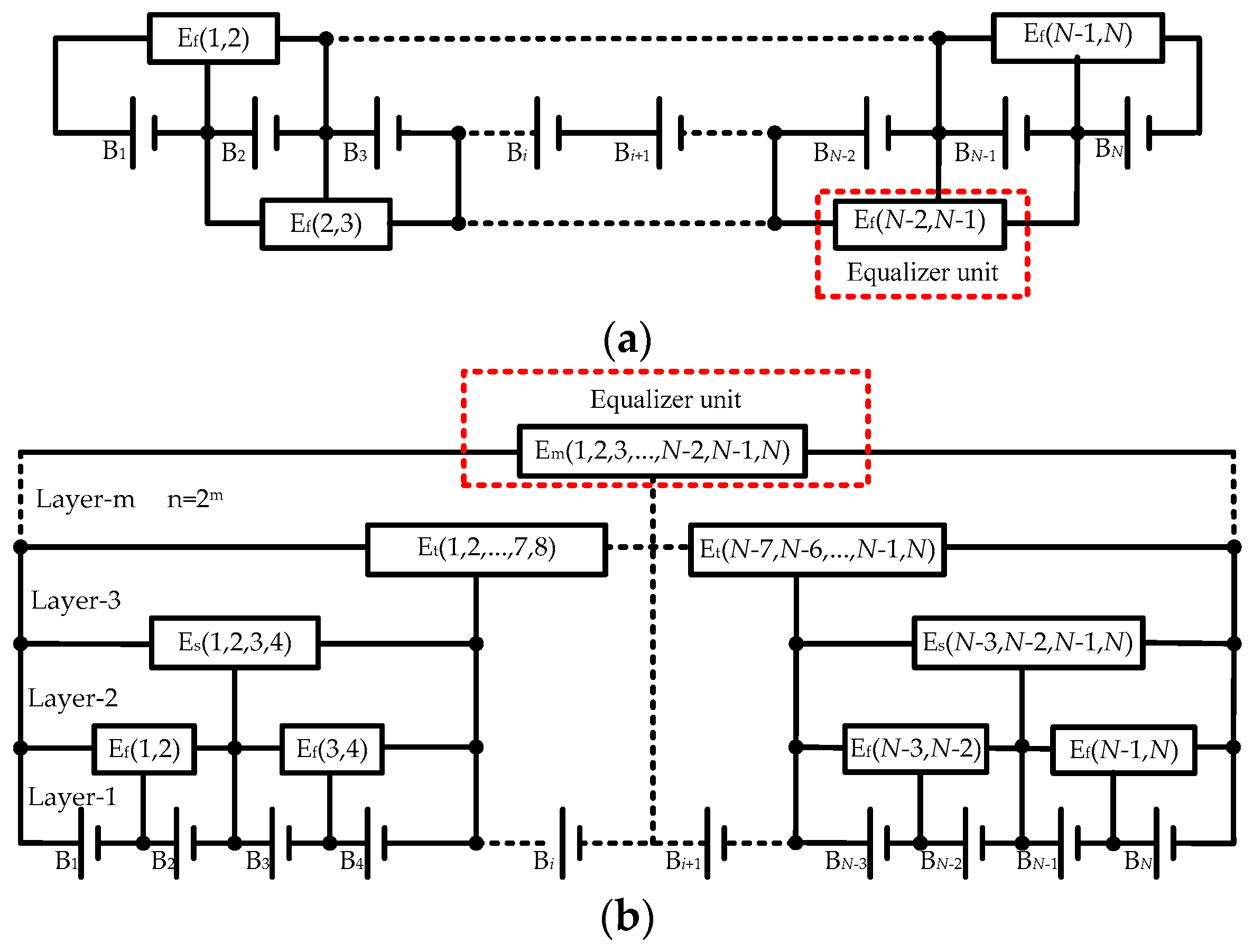
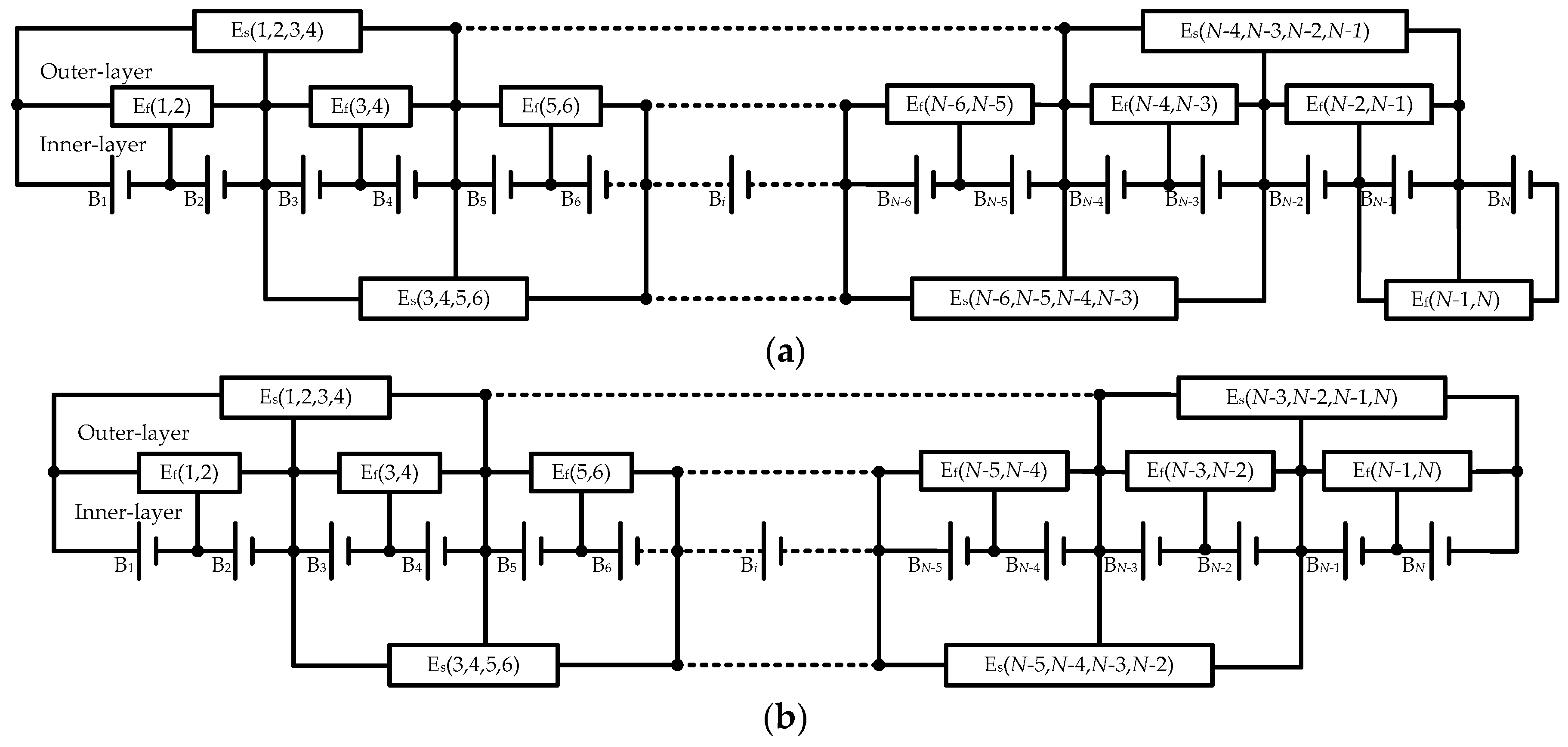
2. Structures of Proposed Equalizer
The structures of proposed equalizer are shown in Figure 2. Figure 2a,b show the odd structure and even structure of proposed equalizer, respectively. The proposed equalizer is composed of the inner-layer equalizer units and the outer-layer equalizer units. Ef (i, i + 1) represents the inner-layer equalizer unit and it equalizes the cells Bi and Bi+1. Es (j, j + 1, j + 2, j + 3) represents outer-layer equalizer unit and it equalizes the cell substrings (Bi, Bi+1) and (Bi+2, Bi+3).
When cell number N is odd, the inner-layer equalizer units of proposed equalizer include Ef (1, 2), Ef (3, 4), …, Ef (i, i + 1), …, Ef (N − 2, N − 1), Ef (N − 1, N) and its outer-layer equalizer units include Es (1, 2, 3, 4), Es (3, 4, 5, 6), …, Es (j, j + 1, j + 2, j + 3), …, Es (N − 4, N − 3, N − 2, N − 1). The number of equalizer units can be expressed as
where Nf and Ns are the number of inner-layer and outer-layer equalizer units, respectively.
When N is even, the inner-equalizer units of proposed equalizer include Ef (1, 2), Ef (3, 4), …, Ef (i, i + 1),…, Ef (N − 1, N), and its outer-layer equalizer units include Es (1, 2, 3, 4), Es (3, 4, 5, 6), …, Es (j, j + 1, j + 2, j + 3), …, Es (N − 3, N − 2, N − 1, N). The number of equalizer units can be expressed as
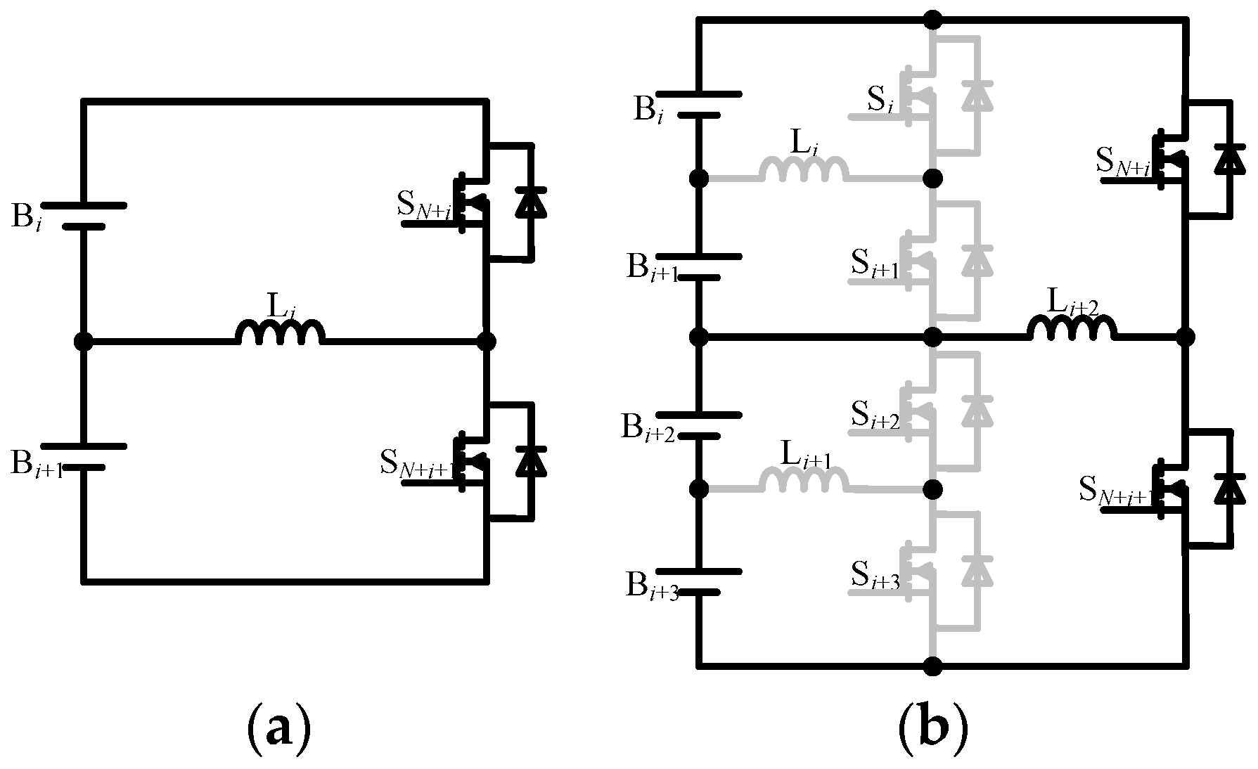
Each equalizer unit of proposed equalizer is a bidirectional buck–boost converter, as shown in Figure 3. Figure 3a shows an inner-layer equalizer unit that equalizes two adjacent cells; Figure 3b shows an outer-layer equalizer unit that equalizers two adjacent cell substrings. The proposed equalizer is composed of (2N − 2) switches (inner-layer switches: S1–SN, outer-layer switches: SN+1–S2N-2) and (N − 1) inductors, as many as the traditional AC2C equalizer. In addition, similar to the parallel structure equalizer, the proposed equalizer provides flexible equalization paths, which reduces equalization time and improves equalization efficiency.
To facilitate the analysis, several assumptions are made as follows:
- All diodes, switches, and inductors employed in proposed equalizer are ideal;
- Each inductor has the identical parameter, i.e., L = L1 = L2 = L3 = … = L2N-2;
- Cell voltages are constant during one switching period;
- All of the buck–boost converters are operated in discontinuous conduction mode (DCM)
3. Equalization Principles
The equalization process of the proposed equalizer consists of two stages. In the first stage, the energy is transferred among adjacent cell substrings and between two cells in a substring by corresponding outer-layer and inner-layer equalizer units, respectively. It is noted that, when N is odd, the energy can also be transferred between cells BN and BN-1, which are adjacent cells but belong to different substrings. In the second stage, the energy is transferred from the maximum voltage cell to the minimum voltage cell, which is implemented by multiple inner-layer and outer-layer equalizer units. By the first stage equalization process, adjacent cell substrings and two cells in a substring are equalized, but the imbalance among cells in the whole battery string is still large. The second stage equalization can realize the equalization of the battery string with small maximum voltage gap among cells, but its equalization speed is slower. Thus, the proposed equalization control strategy combines the first with second stage equalization, which has advantages of both the first and second stage equalization.
3.1. First Stage Equalization
In the first stage equalization, the inner-layer equalizer and outer-layer equalizer work independently. The operation of the equalizer is based on the voltage gap between two adjacent cells or cell substrings. The equalizer has two predefined equalization thresholds; one predefined threshold ∆V for the inner-layer equalizer unit and one predefined threshold 2∆V for out-layer equalizer unit. If the voltage gap is less than the predefined equalization threshold, the corresponding equalizer unit stops working. The working condition of inner-layer equalizer unit can be expressed as
where VBi is the voltage of cell Bi. The working condition of outer-layer equalizer unit can be expressed as
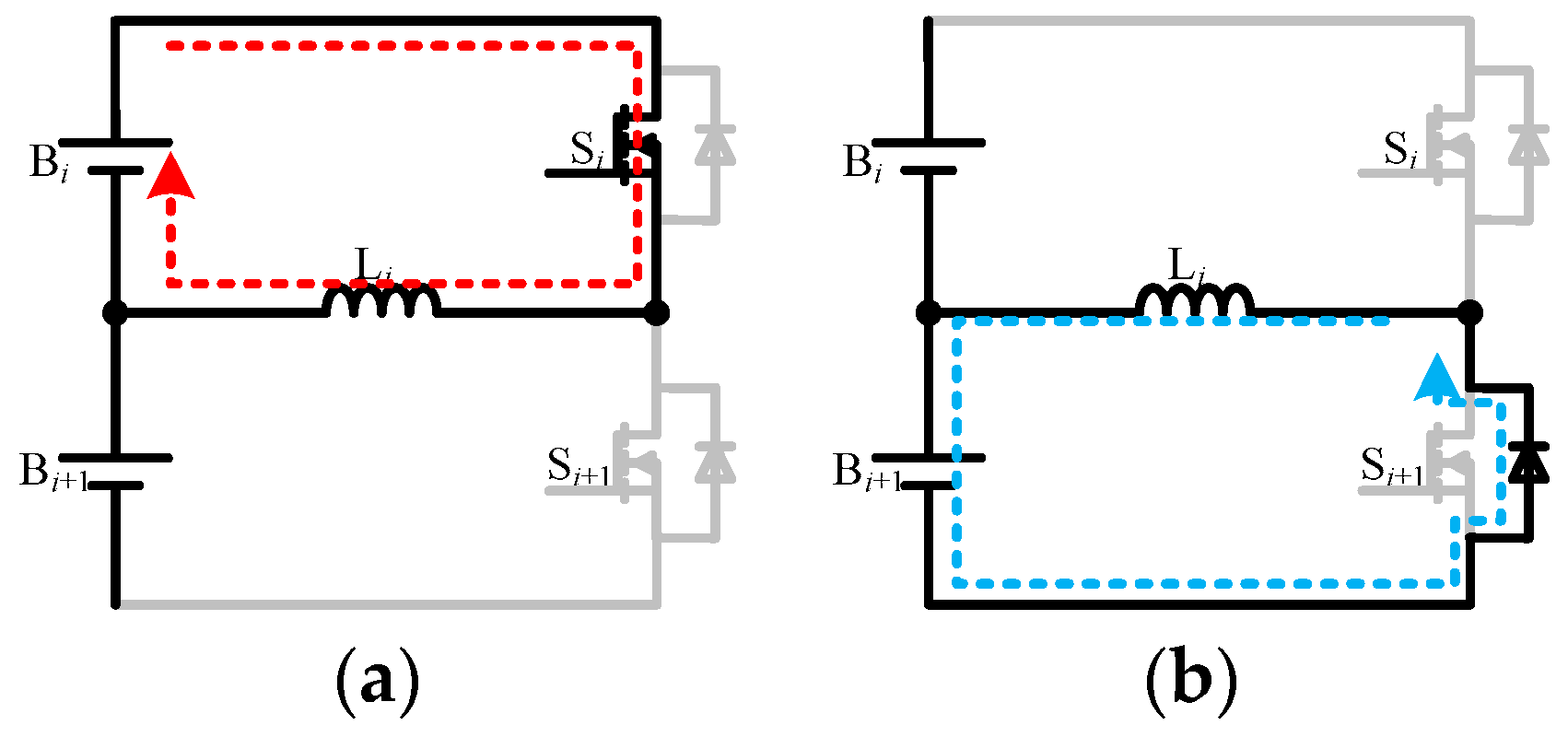
When both the inner-equalizer unit and outer-layer equalizer unit stop working, the equalization process ends. During this stage, the operation principles of inner-layer and outer-layer equalizer units are similar. For the sake of simplification, take inner-equalizer unit as an example to analyze the working process. Assuming that cell voltage VBi is higher than cell voltage VBi+1. The equalization process of this stage includes two modes, i.e., Mode 1 and Mode 2. The current paths of the first stage equalization during different modes are shown in Figure 4.
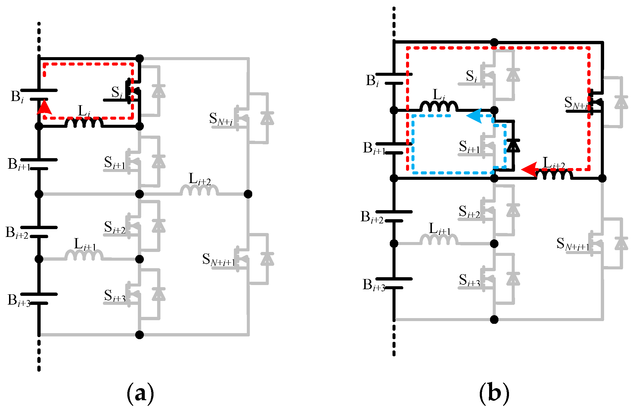
Mode 1 [t0–t1]: Bi discharges.
Figure 4a presents the inductor current path of Mode 1. Mode 1 starts when the switch Si is turned on and the switch Si+1 is turned off. Then, VBi is directly applied to the terminal of the inductor Li, and the inductor current iLi is built up. During this mode, Li is charged by cell Bi and iLi increases linearly. Therefore, iLi can be expressed as
The energy Wi is transferred from cell Bi to Li, and it can be expressed as
In the Formula (6), Di is the duty cycle of the switch Si, and Ts is the switching period.
Mode 2 [t1–t2]: Bi+1 charges.
Figure 4b presents the inductor current path of Mode 2. Mode 2 begins when the switches Si and Si+1 are turned off. The inductor current is commutated from Si to the parasitic diode of Si+1, and it decreases linearly due to the cell voltage is applied to the inductor in the opposite direction. During this mode, the energy is transferred into cell Bi+1 and VBi+1 increases slowly. iLi can be expressed as
When iL reduces to zero, the energy transportation will be stopped by the parasitic diode of Si+1. The freewheeling time Td of iL can be expressed as
In order to avoid magnetic saturation of inductors, the duty cycle of all switches should be designed to satisfy the following expression
The normal voltage range of lithium-ion battery is 2.8–4.2 V, so the duty cycle of all switches must be less than 0.4 to avoid magnetic saturation.
3.2. Second Stage Equalization
The second stage equalization forms an equivalent equalization path by controlling the conduction of the switches and regulating specific duty cycle to achieve equalization between the maximum voltage cell and minimum voltage cell. The second stage equalization includes three modes: Mode 1, the energy transfers from the maximum voltage cell to outer-layer inductor; Mode 2, the energy flows among outer-layer inductors; Mode 3, the energy transfers from outer-layer inductor to the minimum voltage cell. The paper takes even structure of proposed equalizer as an example to elaborate the operation process of the second stage equalization. It is supposed that the voltage of cell Bi is maximum and the voltage of cell Bj is minimum.
Mode 1: the energy transfers from the maximum voltage cell to outer-layer inductor.
Whether switches work or not in equalization process is related to the position of maximum voltage cell Bi in Mode 1, and the corresponding relationship is shown in Table 1. The energy transfer process consists of two parts in Mode 1: (a) the maximum voltage cell Bi discharges; (b) the outer-layer inductor Li+2 charges. The two parts are presented in Figure 5.
As shown in Figure 5a, when the inner-layer switch Si is turned on, the analysis process is the same as the first stage equalization, the energy that stored in Li can be obtained from Formula (6). When Si is turned off, the inductor current iLi flows from the parasitic diode of Si+1 to the adjacent cell Bi+1. The equalizer unit transfers the excess energy from the highest voltage cell Bi to the adjacent cell Bi+1. On the other hand, as shown in Figure 5b, when the outer-layer switches SN+i is turned on, the cell Bi+1 charges the outer-layer inductor Li+2. The energy Wri+1 transfers from cell Bi+1 to Li+2 can be expressed as
If the energy of cell Bi+1 maintains dynamic balance in the process of charging and discharging, the process transfers excess energy from cell Bi to Li+2, and the energy of cell Bi+1 is unchanged. The corresponding energy relationship can be expressed as
From Formula (11), the duty cycle DN+i of SN+i can be obtained as
In addition, the energy WLi+2 transferred from the cell substring (Bi, Bi+1) to Li+2 during this process can be expressed as
Mode 2: the energy flows among outer-layer inductors.
Whether switches work or not in equalization process is related to the position of maximum voltage cell Bi and minimum voltage cell Bj in Mode 2, and the corresponding relationship is shown in Table 2. In addition, the energy transfer process consists of three parts in Mode 2: (a) the outer-layer inductor Li+2 discharges; (b) the outer-layer inductor Li+3 charges; (c) the outer-layer inductor Lj+1 charges. The three parts are presented in Figure 6.
As shown in Figure 6a, when the switch SN+i is turned off, Li+2 charges the adjacent cell substrings through the parasitic diode of switch SN+i+1 to realize the energy transfer from Li+2 to the cell substring (Bi+2, Bi+3). Then, as shown in Figure 6b, when the outer-layer switch SN+i+2 is turned on, the cell substring (Bi+2, Bi+3) charges the outer-layer inductor Li+3. In this process, the energy WLi+3 transfers from the cell substring (Bi+2, Bi+3) to Li+3, which can be expressed as
If the energy of cell substring (Bi+2, Bi+3) maintains dynamic balance in the process of charging and discharging, the mode transfers excess energy from cell Bi to Li+3, and the energy of cell substring (Bi+2, Bi+3) is unchanged in this process. The corresponding energy relationship can be expressed as
From Formula (15), the duty cycle DN+i+2 of SN+i+2 can be expressed as
Similarly, owing to the unchanged energy of intermediate cell substrings in this mode, it means that the duty cycle of the corresponding switches can be solved. Meanwhile, the energy that stored in the inductor Lj-2 can be obtained from Formula (6). When the outer-layer switch SN+j-4 is turned off, the inductor Lj-2 charges the cell substring (Bj-2, Bj-1) through the parasitic diode of switch SN+j-3. Then, as shown in Figure 6c, when the switch SN+j-2 is turned on, the cell substring (Bj-2, Bj-1) charges the outer-layer inductor Lj+1. Similar to the above Formulas (13), (14), (15), duty cycle DN+j-2 of SN+j-2 can be expressed as
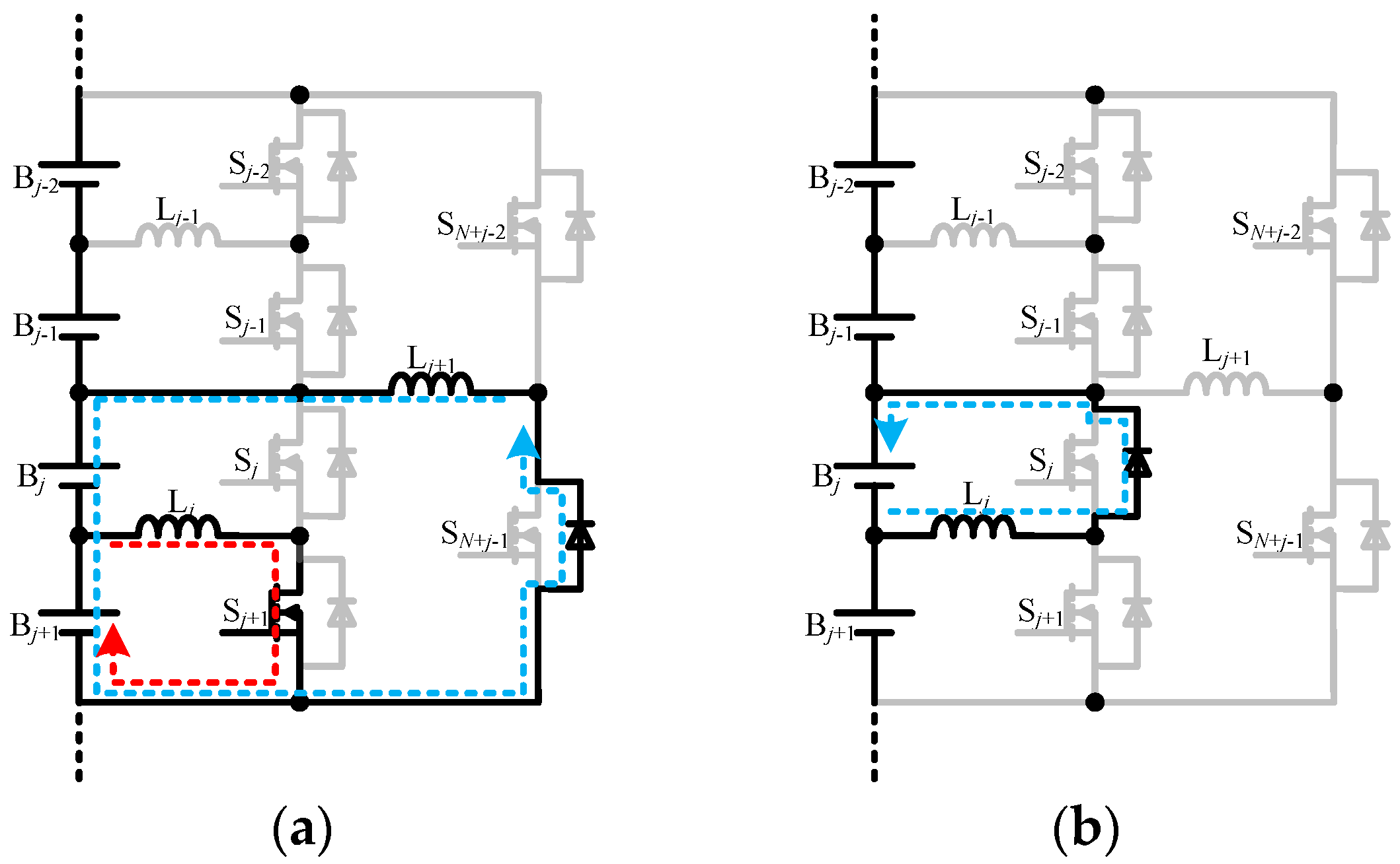
Mode 3: the energy transfers from outer-layer inductor to the minimum voltage cell.
Whether switches work or not in equalization process is related to the position of maximum voltage cell Bi in Mode 3, and the corresponding relationship is shown in Table 3. In addition, the energy transfer process consists of two parts in Mode 3: (a) the outer-layer inductor Lj+1 discharges; (b) the minimum voltage cell Bj charges. The two parts are presented in Figure 7.
To simplify the analysis, it is assuming that all components is ideal, then the energy loss of the whole equalization process can be ignored. The energy transfers from the cell Bi to the inductor Lj+1 can be obtained from the Formula (13). As shown in Figure 7a, when SN+j-2 is turned off, the inductor current iLj+1 commutated from SN+j-2 to parasitic diode of outer-layer switch SN+j-1, and the outer-layer equalizer unit transfers energy from Lj+1 to the cell substring (Bj, Bj+1). According to voltage-divider theorem, the energy Wsj+1 transferred from Lj+1 to the cell Bj+1 can be expressed as
On the other hand, when the inner-layer switch Sj+1 is turned on, cell Bj+1 charges the inner-layer inductor Lj. The energy Wrj+1 transferred from the cell Bj+1 to Lj can be expressed as
If the energy of cell Bj+1 maintains dynamic balance in the process of charging and discharging, the mode transfers excess energy from the maximum voltage cell Bi to Lj, and the energy of cell Bj+1 is unchanged in this process. The corresponding energy relationship can be expressed as
From Formulas (18), (19), and (20), the duty cycle Dj+1 of Sj+1 can be expressed as
As shown in Figure 7b, when Sj+1 is turned off, Lj charges the cell Bj through the parasitic diode of inner-layer switch Sj to realize the energy transfer from Lj to cell Bj.
In fact, the energy transfers from the maximum voltage cell Bi to the minimum voltage cell Bj by the second stage equalization, and the energy of other cells are unchanged. Thus, the second stage equalization decreases the maximum voltage gap between maximum voltage and minimum voltage in the battery string.
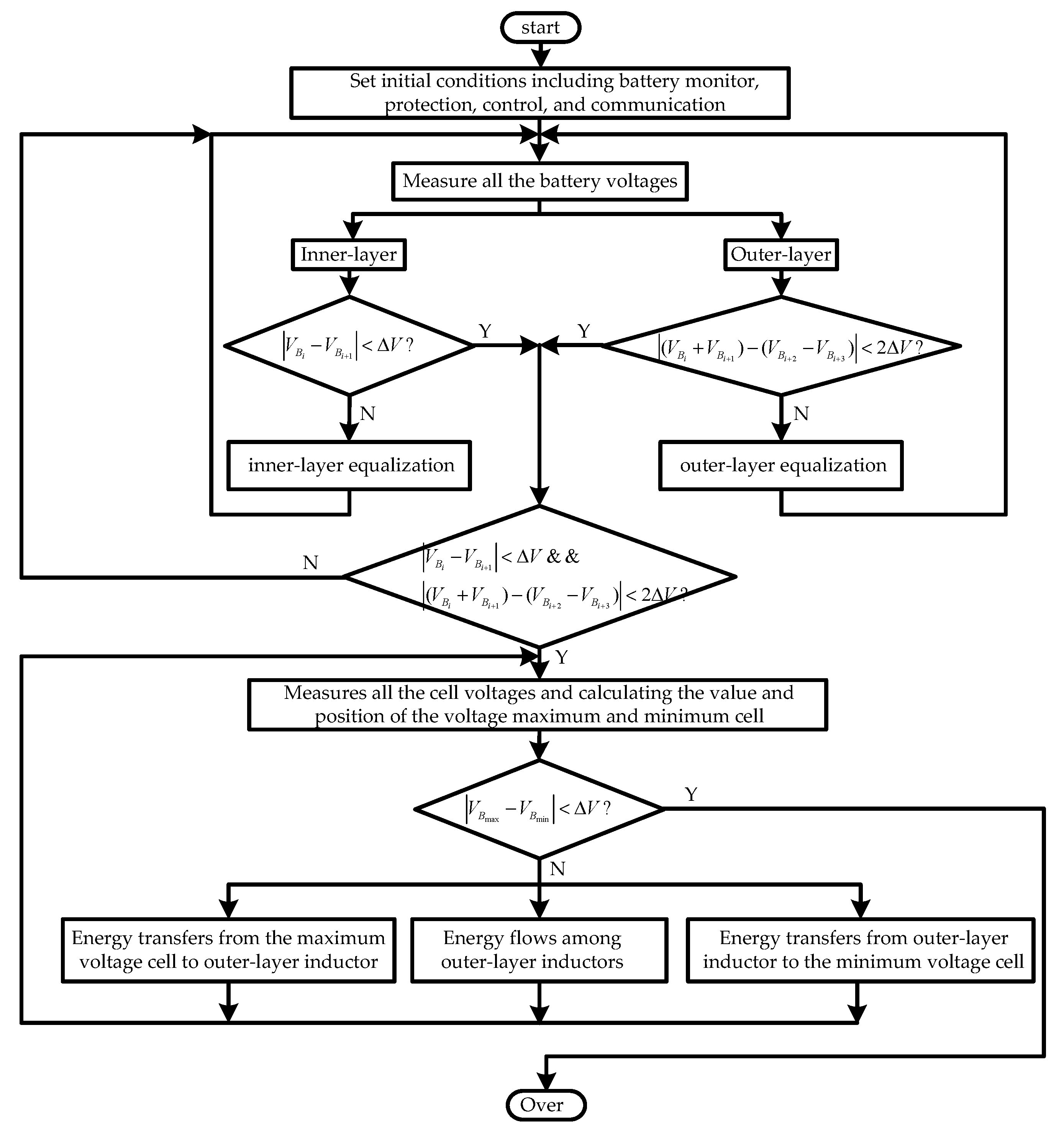
4. Equalization Control Strategy
The paper proposes a two stages equalization control strategy. The first stage equalization is widely used in traditional equalizers, it has the advantages of fast equalization speed and simply control, but it has the disadvantage of repeated flow of energy. Meanwhile, the maximum voltage gap after balancing among cells is increased with the increase of N due to the accumulation of threshold voltage gap of equalizers. Especially for AC2C equalizer, if the voltage gap of two adjacent cells is less than the predefined threshold, then in the worst case, the maximum voltage gap between maximum voltage and minimum voltage in the battery string can be expressed as
The increase of maximum voltage gap after balancing among cells affects the equalization performance, which will decrease the total storage capacity and battery lifecycle. Meanwhile, if the given threshold is reduced, although the maximum voltage gap will also decrease, the corresponding equalization time will be greatly increased. Therefore, the second stage equalization is proposed to decrease the maximum voltage gap.
The flow chart of the proposed equalization control strategy used in simulations and experiments is show in Figure 8. When the arbitrary equalizer unit detects that two adjacent cells or cell substrings voltage gap is greater than the predefined threshold, the first stage equalization starts working. On the contrary, when all equalization units detect that the adjacent voltage gap is less than the given threshold, the first stage equalization stops working. Unfortunately, the maximum voltage gap is still large after finishing the first stage equalization, the equalizer begins the second stage equalization, and it stops working until the maximum voltage gap is less than the predefined threshold. Thus, the proposed control strategy can improve equalization performance.
5. Simulation
In order to compare the equalization performance of proposed equalizer with AC2C equalizer, the simulations for six cells at six different initial voltage distributions were carried out using PSIM software. Table 4 shows the initial voltage distributions of six cells.
As shown in Table 4, at different cases, the maximum voltage gaps among cells are 0.59 V. In simulation, the switching frequency was set as 10 kHz, and the value of each inductor is 100 μH and duty cycle was set as 0.4. In addition, energy storage cells B1–B6 were replaced by capacitors (0.1F). The paper compares three equalizers by simulation: AC2C equalizer, DLE equalizer with first stage equalization (DLE1 equalizer), and DLE equalizer with the proposed two-stage equalization (DLE2 equalizer). For the AC2C equalizer, simulation and experimental voltage thresholds are set to 10 mV. For DLE1 equalizer, the inner-layer voltage threshold was set as 10 mV and outer-layer voltage threshold was set as 20 mV. Furthermore, for DLE2 equalizer, the maximum voltage gap of the whole battery pack was set as 10 mV.
The three equalizers are simulated using identical voltage distribution and parameters. Under the condition of six cells, the number of different initial voltage distribution sequences is . It is almost impossible to simulate those distributions one by one. However, for DLE equalizer, six cells can be divided into three substrings that include two adjacent cells, so the paper compares six different voltage distributions due to .
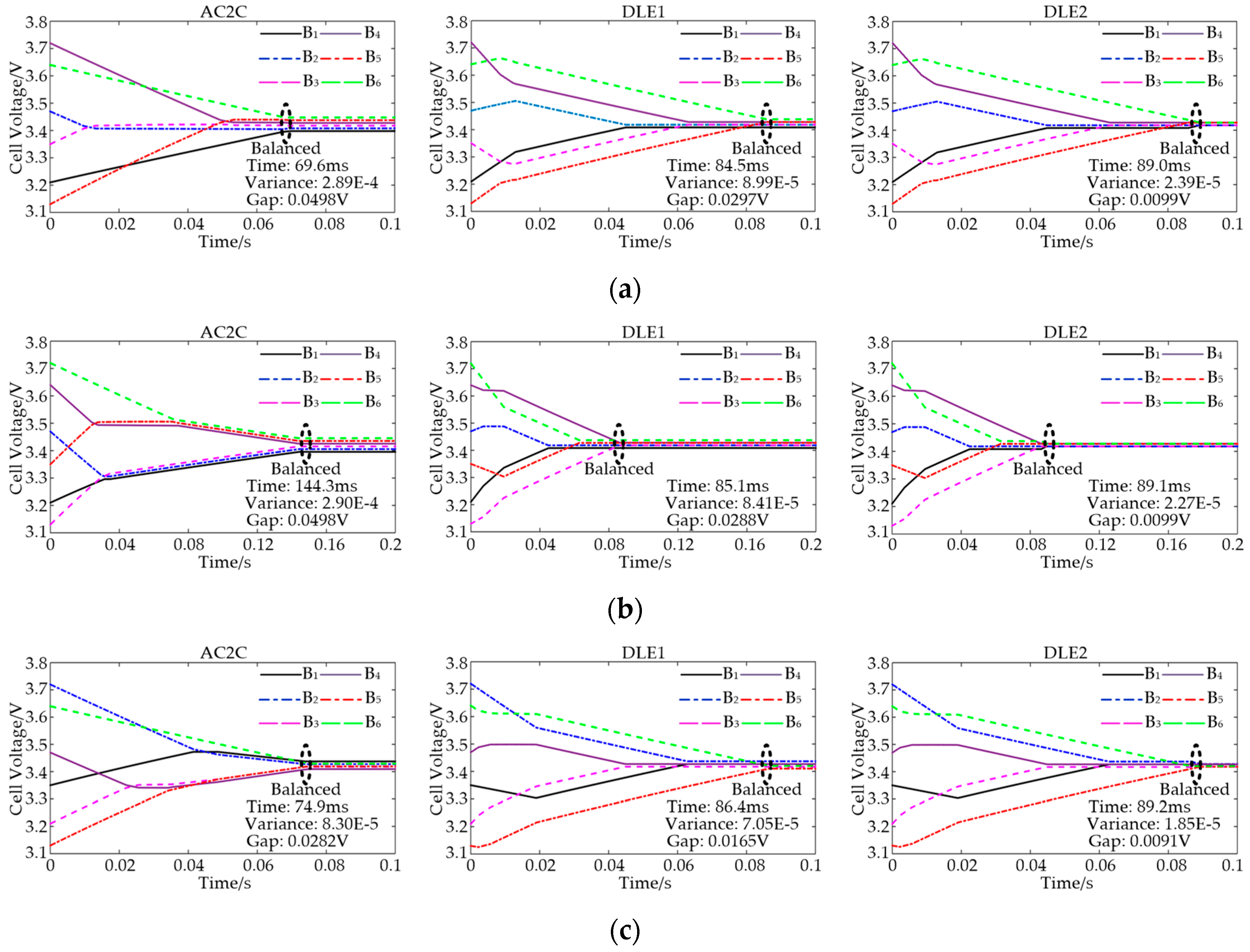
The simulation results are shown in Figure 9. From the simulation results, at six different initial voltage distributions, DLE2 equalizer has controllable maximum voltage gap compared to the other equalizers. Furthermore, the DLE equalizer has a relatively stable equalization time than AC2C equalizer in different distribution sequences of the cell voltage, it means that DLE equalizer has more stable equalization performance.
The paper also defines voltage variance and maximum voltage gap as extra index for further evaluate the equalization performance.
The variance σ2 is defined as
where is the average voltage of cells in the battery string. The smaller σ2 is, the better equalization performance is.
The maximum voltage gap Vgap in the battery string is defined as
where VBmax is maximum voltage in the battery string and VBmin is minimum voltage in the battery string. Similarly, the smaller Vgap is, the better equalization performance is.
Table 5 shows the average equalization performance of six simulation results. The DLE1 and DLE2 equalizers have shorter average equalization time, smaller voltage variance, and smaller maximum voltage gap compare with AC2C equalizer, which further proves that DLE1 and DLE2 equalizers have superior equalization performance. As N grows, the advantages of DLE1 and DLE2 equalizers will become more and more obvious. In addition, although the average equalization time of DLE2 equalizer increases slightly compared with DLE1 equalizer, the voltage variance and the maximum voltage gap is significant declined.
6. Experimental Results
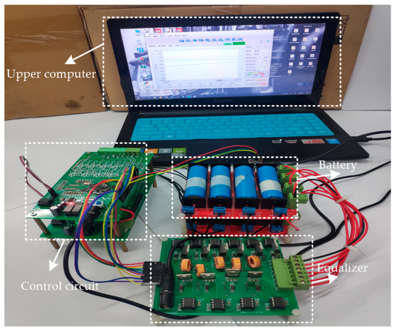
In order to verify the analysis and simulation results in above sections, experiments were carried out by using lithium-ion battery string containing six cells connected in series. Figure 10 shows a photograph of the experimental circuit. The acquisition chip is the sensor to make measurement on the status of the battery cell. The monitoring IC reads the voltage value of the cells and communication with the microcontroller. The microcontroller collects data and sends it to upper computer. The microcontroller comparers the result with the threshold value set, detects the unbalanced cell and generates pulse width modulation (PWM) signals to drive the corresponding MOSFET according to the proposed algorithm. Figure 10 shows a photograph of the experimental circuit and Table 6 shows the specification of component used for experiments.
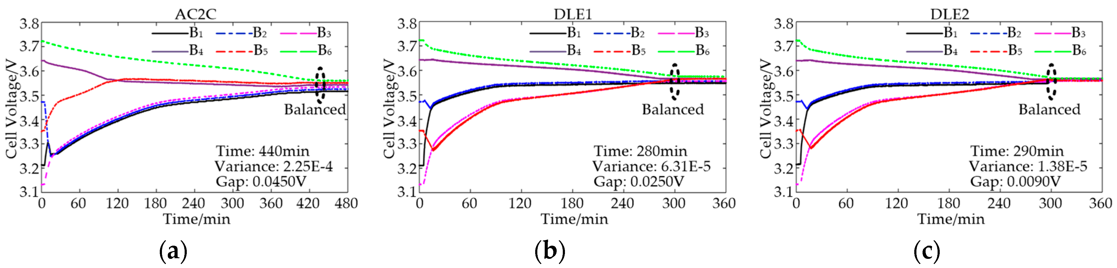
Figure 11 shows the experimental results for six cells under the condition of Case 2 of Table 4. The operating conditions of AC2C equalizer and the proposed equalizers are the same as the simulation. As shown in Figure 11, three equalizers can realize the equalization of battery string, but their balancing time is different. The AC2C equalizer takes 440 min. However, the proposed equalizers require only 280 min and 290 min. Thus, the equalization speed of the proposed equalizers is better than that of the conventional AC2C equalizer. In addition, the maximum voltage gap of conventional AC2C equalizer is 0.045 V after the total equalization process. The maximum voltage gap of DLE1 equalizer is 0.025 V after balancing, and it is reduced by 55.6% compared with AC2C equalizer. For the DLE2 equalizer, although the equalization time equalizer increases slightly compared with DLE1 equalizer, the maximum voltage gap is reduced from 0.025 V to 0.009 V, which is the minimum among three equalizers. Meanwhile, the voltage variance of the proposed equalizers is smaller than the AC2C equalizer.
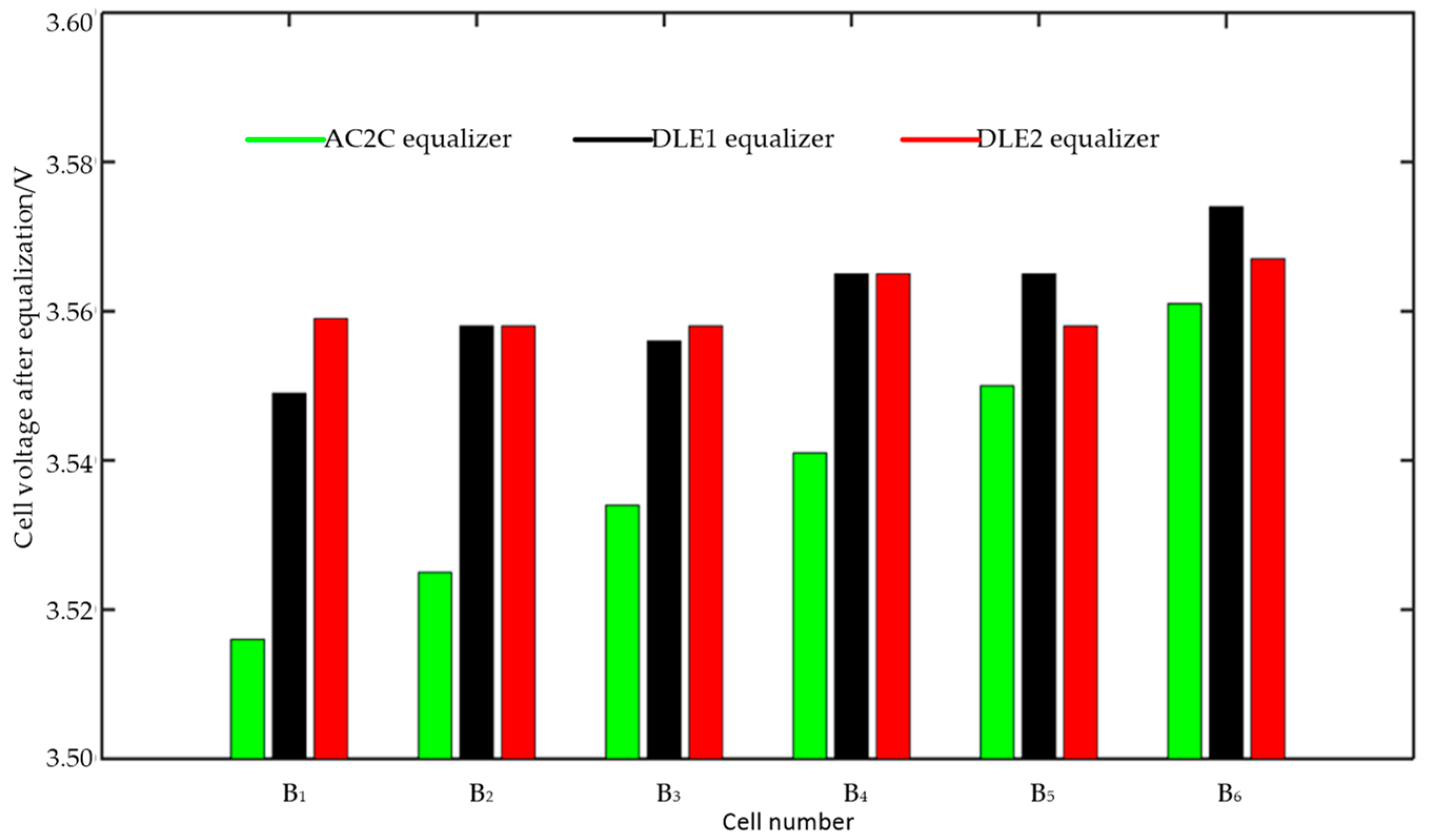
Figure 12 shows the cell voltage distributions of three equalizers after balancing. Among them, the maximum voltage gap of the DLE2 equalizer is minimum, followed by DLE1 equalizer, and the maximum voltage gap of the AC2C equalizer is maximum. Thus, it is further demonstrated that the proposed equalizers can achieve better equalization performance.
In summary, DLE1 and DLE2 equalizers realize better equalization performance compared with AC2C equalizer. In addition, the DLE2 equalizer decreases efficiency and speed a little compared with the DLE1 equalizer due to adding second stage equalization, but the maximum voltage gap and variance are minimum of the DLE2 equalizer among three equalizers. Furthermore, the maximum voltage gap of the DLE2 equalizer is controllable and does not increase as N increases. It means that the DLE2 equalizer can better prolong battery lifecycle and available capacity compared with the AC2C equalizer and the DLE1 equalizer. However, as in any engineering problem, the DLE2 equalizer exists as a tradeoff. The DLE2 equalizer increases equalization performance, but it also increases complexity of the control strategy compared with the AC2C equalizer and DLE1 equalizer.
7. Conclusions
This paper proposes a new double-layer E-structure (DLE) equalizer for battery voltage equalization, in which the equalization time can be decreased compared with AC2C equalizer. In addition, a novel two-stage control strategy is proposed to decrease the maximum voltage gap. The novel control strategy is very useful to meet higher cell voltage consistency. Furthermore, simulations and experiments are used to verify the validity of the proposed equalizer and control strategy. Thus, it is anticipated that the proposed equalizer and control strategy will allow important improvements in the performance of energy storage systems.
Author Contributions
This research article has four authors. The circuit structure and control strategy were designed by S.X. and K.G. X.Z., K.L. and K.G. conceived the research methods. S.X. contributed the experimental environment. K.G. wrote the paper. X.Z. and S.X. revised the paper and provided some helpful suggestions.
Funding
This research was supported by Sichuan Science and Technology Program under Grants (61371033). The authors would like to thank them for their support and help. The authors would also like to thank the reviewers for their corrections and helpful suggestions.
Conflicts of Interest
The authors declare no conflict of interest.
References
- Cassani, P.; Williamson, S. Significance of battery cell equalization and monitoring for practical commercialization of plug-in hybrid electric vehicles. In Proceedings of the 2009 Twenty-Fourth Annual IEEE Applied Power Electronics Conference and Exposition, Washington, DC, USA, 15–19 February 2009; pp. 4654–4671. [Google Scholar]
- Chan, C.; Chau, K. An overview of electric vehicles-challenges and opportunities. In Proceedings of the 22nd International Conference on Industrial Electronics, Control, and Instrumentation, Taipei, Taiwan, 9–9 August 1996; pp. 1–6. [Google Scholar]
- Cao, J.; Schofield, N.; Emadi, A. Battery balancing methods: A comprehensive review. In Proceedings of the 2008 IEEE Vehicle Power and Propulsion Conference, Harbin, China, 3–5 September 2008; pp. 1–6. [Google Scholar]
- Linzen, D.; Buller, S.; Karden, E.; Doncker, R.W.D. Analysis and evaluation of charge balancing circuits on performance, reliability and lifetime of supercapacitor systems. IEEE Trans. Ind. Appl. 2005, 41, 1135–1141. [Google Scholar] [CrossRef]
- Daowd, M.; Omar, N.; Bossche, P.V.D.; Mierlo, J.V. A review of passive and active battery balancing based on Matlab/Simulink. In Proceedings of the 2011 IEEE Vehicle Power and Propulsion Conference, Chicago, IL, USA, 6–9 September 2011; pp. 2974–2989. [Google Scholar]
- Lindemark, B. Individual cell voltage equalizers (ICE) for reliable battery performance. In Proceedings of the Thirteenth International Telecommunications Energy Conference-INTELEC 91, Kyoto, Japan, 5–8 November 1991; pp. 196–201. [Google Scholar]
- Pascual, C.; Krein, P. Switched capacitor system for automatic series battery equalization. In Proceedings of the Applied Power Electronics Conference, Atlanta, GA, USA, 27 February 1997; pp. 848–854. [Google Scholar]
- Ye, Y.; Cheng, K.W.E. An automatic switched-capacitor cell balancing circuit for series-connected battery string. Energies 2016, 9, 138. [Google Scholar] [CrossRef]
- Kim, M.; Kim, C.; Kim, J.; Moon, G. A chain structure of switched capacitor for improved cell balancing speed of lithium-ion batteries. IEEE Trans. Ind. Electron. 2014, 61, 3989–3999. [Google Scholar] [CrossRef]
- Kutkut, N.; Wiegman, H.; Divan, D.; Novotny, D. Design considerations for charge equalization of an electric vehicle battery system. IEEE Trans. Ind. Appl. 1999, 35, 28–35. [Google Scholar] [CrossRef] [Green Version]
- Cassani, P.A.; Williamson, S.S. Design, testing, and validation of a simplified control scheme for a novel plug-in hybrid electric vehicle battery cell equalizer. IEEE Trans. Ind. Electron. 2010, 57, 3956–3962. [Google Scholar] [CrossRef]
- Guo, X.; Kang, L.; Huang, Z.; Yao, Y.; Yang, H. Research on a novel power inductor-based bidirectional lossless equalization circuit for series-connected battery packs. Energies 2015, 8, 5555–5576. [Google Scholar] [CrossRef]
- Wang, S.; Kang, L.; Guo, X.; Wang, Z.; Liu, M. A novel layered bidirectional equalizer based on a buck-boost converter for series-connected battery strings. Energies 2017, 10, 1011. [Google Scholar] [CrossRef]
- Peng, F.; Wang, H.; Yu, L. Analysis and design considerations of efficiency enhanced hierarchical battery equalizer based on bipolar CCM buck-boost unit. IEEE Trans. Ind. Appl. 2019, 55, 4053–4063. [Google Scholar] [CrossRef]
- Kim, M.; Kim, J.; Moon, G. Center-cell concentration structure of a cell-to-cell balancing circuit with a reduced number of switches. IEEE Trans. Power Electron. 2014, 29, 5285–5297. [Google Scholar] [CrossRef]
- Dong, B.; Li, Y.; Han, Y. Parallel architecture for battery charge equalization. IEEE Trans. Power Electron. 2015, 30, 4906–4913. [Google Scholar] [CrossRef]
- Lee, K.; Lee, S.; Choi, Y.; Kang, B. Active balancing of Li-Ion battery cells using transformer as energy carrier. IEEE Trans. Ind. Electron. 2017, 64, 1251–1257. [Google Scholar] [CrossRef]
- Park, H.; Kim, J.; Kim, C.; Moon., G.; Lee, J. A modularized charge Equalizer for an HEV lithium-ion battery string. IEEE Trans. Ind. Electron. 2009, 56, 1464–1476. [Google Scholar] [CrossRef]
- Uno, M.; Kukita, A. String-to-battery voltage equalizer based on a half-bridge converter with multistacked current doublers for series-connected batteries. IEEE Trans. Power Electron. 2019, 34, 1286–1298. [Google Scholar] [CrossRef]
Figure 1.
AC2C equalizer and parallel structure equalizer. (a) AC2C equalizer; (b) parallel structure equalizer.
Figure 1.
AC2C equalizer and parallel structure equalizer. (a) AC2C equalizer; (b) parallel structure equalizer.

Figure 2.
Structures of proposed equalizer. (a) Odd structure of proposed equalizer. (b) Even structure of proposed equalizer.
Figure 2.
Structures of proposed equalizer. (a) Odd structure of proposed equalizer. (b) Even structure of proposed equalizer.

Figure 3.
Equalizer unit. (a) Inner-layer equalizer unit. (b) Outer-layer equalizer unit.

Figure 4.
Current paths of the first stage equalization during different modes. (a) Mode 1, Bi discharges; (b) Mode 2, Bi+1 charges.
Figure 4.
Current paths of the first stage equalization during different modes. (a) Mode 1, Bi discharges; (b) Mode 2, Bi+1 charges.

Figure 5.
Current paths of second stage equalization in Mode 1. (a) The maximum voltage cell Bi discharges. (b) The out-layer inductor Li+2 charges.
Figure 5.
Current paths of second stage equalization in Mode 1. (a) The maximum voltage cell Bi discharges. (b) The out-layer inductor Li+2 charges.

Figure 6.
Current paths of the second stage equalization in Mode 2. (a) Outer-layer inductor Li+2 discharges. (b) Outer-layer inductor Li+3 charges. (c) Outer-layer inductor Lj+1 charges.
Figure 6.
Current paths of the second stage equalization in Mode 2. (a) Outer-layer inductor Li+2 discharges. (b) Outer-layer inductor Li+3 charges. (c) Outer-layer inductor Lj+1 charges.

Figure 7.
Current paths of the second stage equalization in Mode 3. (a) Outer-layer inductor Lj+1 discharges. (b) Minimum voltage cell Bj charges.
Figure 7.
Current paths of the second stage equalization in Mode 3. (a) Outer-layer inductor Lj+1 discharges. (b) Minimum voltage cell Bj charges.

Figure 8.
Flow chart of proposed equalization control strategy used in simulations and experiments.

Figure 9.
Simulation results of different initial voltage distribution. (a) Case 1; (b) Case 2; (c) Case 3; (d) Case 4; (e) Case 5; (f) Case 6.
Figure 9.
Simulation results of different initial voltage distribution. (a) Case 1; (b) Case 2; (c) Case 3; (d) Case 4; (e) Case 5; (f) Case 6.


Figure 10.
Photograph of the experimental circuit.

Figure 11.
Experimental results of three equalizers for six cells under the condition of Case 2 of Table 4. (a) AC2C; (b) DLE1; (c) DLE2.
Figure 11.
Experimental results of three equalizers for six cells under the condition of Case 2 of Table 4. (a) AC2C; (b) DLE1; (c) DLE2.

Figure 12.
Cell voltage distributions of three equalizers after balancing.


Table 1.
Switches working in Mode 1
| i | Odd Number | Even Number | |
|---|---|---|---|
| Layer | |||
| Inner-layer | |||
| Outer-layer | |||
Table 2.
Switches working in Mode 2.
| i | Odd Number | Even Number | |
|---|---|---|---|
| j | |||
| Odd number | |||
| Even number | |||
Table 3.
Switches working in Mode 3
| j | Odd Number | Even Number | |
|---|---|---|---|
| Layer | |||
| Inner-layer | |||
Table 4.
Initial voltage distributions for simulation
| B1 (V) | B2 (V) | B3 (V) | B4 (V) | B5 (V) | B6 (V) | |
|---|---|---|---|---|---|---|
| Case 1 | 3.21 | 3.47 | 3.35 | 3.72 | 3.13 | 3.64 |
| Case 2 | 3.21 | 3.47 | 3.13 | 3.64 | 3.35 | 3.72 |
| Case 3 | 3.35 | 3.72 | 3.21 | 3.47 | 3.13 | 3.64 |
| Case 4 | 3.35 | 3.72 | 3.13 | 3.64 | 3.21 | 3.47 |
| Case 5 | 3.13 | 3.64 | 3.21 | 3.47 | 3.35 | 3.72 |
| Case 6 | 3.13 | 3.64 | 3.35 | 3.72 | 3.21 | 3.47 |
Table 5.
Average equalization performance of six simulation results
| AC2C | DLE1 | DLE2 | |
|---|---|---|---|
| Equalization time (ms) | 90.67 | 85.42 | 88.97 |
| Variance | 2.3×10⁻⁴ | 8.16×10⁻⁵ | 2.17×10⁻⁵ |
| Voltage gap (V) | 0.0421 | 0.0267 | 0.0097 |
Table 6.
Specification of component for experiments
| Parameters | Value | |
|---|---|---|
| Cell balancing circuit | MOSFET | IRF540NPBF |
| Gate driver | HCPL-3120 | |
| Switching frequency | 10 KHz | |
| Inductor | 100 µH | |
| Microcontroller | STM32F103RCT6 | |
| Acquisition chip | LTC6803 | |
| Lithium-ion battery | Nominal capacity | 2 Ah |
| Cell voltage variation | 2.8–4.2 V | |
© 2019 by the authors. Licensee MDPI, Basel, Switzerland. This article is an open access article distributed under the terms and conditions of the Creative Commons Attribution (CC BY) license (http://creativecommons.org/licenses/by/4.0/).
Share and Cite
MDPI and ACS Style
Xu, S.; Gao, K.; Zhang, X.; Li, K. Double-Layer E-Structure Equalization Circuit for Series Connected Battery Strings. Energies 2019, 12, 4252. https://doi.org/10.3390/en12224252
AMA Style
Xu S, Gao K, Zhang X, Li K. Double-Layer E-Structure Equalization Circuit for Series Connected Battery Strings. Energies. 2019; 12(22):4252. https://doi.org/10.3390/en12224252
Chicago/Turabian StyleXu, Shungang, Kai Gao, Xiaobing Zhang, and Kangle Li. 2019. "Double-Layer E-Structure Equalization Circuit for Series Connected Battery Strings" Energies 12, no. 22: 4252. https://doi.org/10.3390/en12224252
Note that from the first issue of 2016, this journal uses article numbers instead of page numbers. See further details here.