Study of Conventional Sintered Cu2Se Thermoelectric Material


Department of Electrical Engineering, The Hong Kong Polytechnic University, Hong Kong
*
Author to whom correspondence should be addressed.
Energies 2019, 12(3), 401; https://doi.org/10.3390/en12030401
Submission received: 12 December 2018
/
Revised: 11 January 2019
/
Accepted: 15 January 2019
/
Published: 27 January 2019
(This article belongs to the Section D1: Advanced Energy Materials)
Abstract
:Lead-free thermoelectric material, copper chalcogenides, have been attracting much interest from many research and industrial applications owing to their high capability of harvesting energy from heat. The state-of-the-art copper chalcogenides are commonly fabricated by the spark plasma sintering (SPS) and hot pressing (HP) techniques. Those methods are still costly and complicated particularly when compared to the conventional solid-state sintering method. Here, we report an easy-to-fabricate lead-free copper(I)-selenium (Cu2Se) that was fabricated using the conventional sintering method. The fabrication conditions, including sintering temperature and dwelling time, have been systematically studied to optimize the thermoelectric performance of Cu2Se. The optimized zT value for the pure Cu2Se was found to be 1.2 for the sample sintered at 1173 K for 2 h. The study shows that Cu2Se developed using the simple and low-cost techniques could exhibit comparable thermoelectric performance when compared with those fabricated by the SPS method, which provides an alternative potential technique to synthesize high-performance thermoelectric materials in a cost-effective way for industrialization.
1. Introduction
Thermoelectric material defines one kind of material specified by the capability of converting heat into electricity directly and vice versa [1,2]. During the past twenty years, this functional material has attracted great interest due to its potential application in the sustainable energy area [3]. To evaluate the performance of thermoelectricity, a figure of merit (zT) is introduced with component parts, Seebeck coefficient (S), electrical conductivity (σ), absolute temperature (T), thermal conductivity (κ), following the relationship of zT = S2σTκ−1 [4].
Among the state-of-the-art excellent thermoelectric materials, copper selenide (Cu2Se) has been widely studied due to its potential of having high zT and its environmentally friendly nature when compared with lead-based thermoelectric materials. The excellent thermoelectric performance of Cu2Se is associated with its superionic behaviour in the high-temperature β-phase such that its theoretical specific heat at constant volume is smaller than that of general solid crystals. This would induce the reduction of specific heat capacity at constant pressure, and thus decrease the thermal conductivity [5]. Recently, studies on Cu2Se have been performed via fabrication techniques using the spark plasma sintering (SPS) technique [5], the hot pressing method [6], the cold quenching method [7], and the nanostructuring method [8], among which the SPS and hot pressing dominate the fabrication methods of Cu2Se. Liu et al., reported the Cu2Se material, fabricated using the SPS method, showed extremely low thermal conductivity and an enhanced zT value of 1.5 [5]. Many other methods have been proposed to enhance the thermoelectric performance of Cu2Se, such as silver doping [9], nanostructured Cu2−xSe [8], and bulk nanocomposites in which nano-inclusions are embedded in bulk matrices [10], etc. Nevertheless, the superionic behavior itself becomes an obstacle to be applied in the thermoelectric devices due to its quick aging during cycling with high current flow. The other reason for the unstable thermoelectric performance arises from the evaporation of Se during the high-temperature cycling [11]. Attempts to resolve the issue include introducing a second phase-like CuInSe2 [12] and enlarging the band gap by the substitution of Cu sites with Li [13] or other dopants such as Sn [14]. Another strategy proposed is to use a blocking layer like carbon to suppress the migration of Cu under high current flow inside the material [15].
Nevertheless, the aforementioned techniques are relatively costly and complicated, especially when compared to the conventional sintering method. The SPS technique features short-time sintering and high sample density, while requiring physical contact with the sample and electrical current excitement during the fabrication process. However, the superionic nature of Cu2Se allows Cu to migrate easily under the high current flow, which is the case during the sintering progress using the SPS technique. This kind of Cu migration in the SPS process has been observed by G. Dennler et al. [16]. Thus, the SPS technique may not be the optimal fabrication method for superionic thermoelectric materials. For the hot press sintering technique, graphite paper is required. Some active metals like lithium could react with graphite. The conventional sintering technique offers an alternative easy way to obtain densified samples without involving the physical excitement or contact of the sample. Besides, the cost would be reduced remarkably if the thermoelectric materials, such as Cu2Se, could be fabricated using the conventional sintering method, which favors its industrialization.
Here, we investigated the thermoelectric properties of the stoichiometric Cu2Se fabricated by the conventional sintering method and explore the influence of sintering temperature and dwelling time on the phase structure, microstructure, and thermoelectric performance of Cu2Se. Finally, the optimized sintering parameters of Cu2Se were determined. The optimized zT value approached 1.2 at 823 K for the samples sintered at 1173 K for two hours.
2. Experimental procedures
2.1. Preparation of Materials
Cu2Se samples were synthesized by the conventional solid-state sintering method. The starting materials, Cu (99.9%) and Se (99.99%), were used and calculated according to the chemical formula of the material. Then, the mixture was sealed in a quartz crucible and sintered at 933 K for 2 h with a protective ultrahigh purity argon atmosphere to obtain the sintered powder. The as-prepared powder was ground into fine powder using an agate jar, weighed, and pressed into discs under a pressure of 240 MPa. Finally, the discs with a diameter of 14 mm were sintered again at 973 K and 1173 K for 2 and 20 h. Consequently, the samples were slowly cooled to the room temperature. The density of the samples was measured using Archimedes’ Principle.
2.2. Characterizations
2.2.1. Powder X-ray Diffraction (XRD)
PXRD patterns were collected using a Rigaku SmartLab diffractometer equipped with a CuKα source. The patterns were collected with a specified scanning step of 0.02° in the range of 20–55°.
2.2.2. Scanning Electron Microscopy (SEM)
SEM was performed using a TESCAN-VEGA3 scanning electron microscope to investigate the microstructure and morphology of the as-prepared Cu2Se samples at room temperature. The samples were cracked in air to explore the fracture morphology. Due to the good electrical conductivity of the as-prepared Cu2Se, the coating of gold (Au) was not implemented before conducting the SEM examinations.
2.3. Thermoelectric Characterization
2.3.1. Seebeck Coefficient and Electrical Conductivity Measurements
The electrical transport properties including the Seebeck coefficient (S) and the electrical conductivity (σ) were measured in a helium atmosphere with the Netzsch SBA458 (Netzsch, Gerätebau GmbH, Germany) instrument system using the four-wire method. The testing temperature ranged from room temperature to 823 K with a step of 50 K. Two pairs of thermocouples and current pins were placed under the sample for the measurements of the Seebeck coefficient and electrical conductivity. The maximum constant current setting was set to 8 mA for the electrical conductivity measurement while the maximum heating voltage was set to 8 V, producing a temperature difference of about 3 K. The furnace was then manually evacuated or filled with inert gas or continuously purged with inert gas. During the test of the Seebeck coefficient, the real-time thermoelectric voltage (V) and temperature (T) were recorded and plotted to obtain the slope of V-T plot. The final Seebeck coefficient was modified according to the following equation:
where and are the slopes in the V-T plot corresponding to the measurement probe types: n type for and p type for . sAB is the contact potential difference of the thermocouple. sA and sB represent the thermoelectric voltage for n-type and p-type thermocouples, respectively.
2.3.2. Thermal Conductivity Measurement
The method for determining the thermal conductivity (κ) is to measure the thermal diffusivity (D), the specific heat (cp) and the geometric density (ρ) as a function of temperature, and then calculate the thermal conductivity using the following equation:
The thermal diffusivity was measured in an argon atmosphere by a Netzsch LFA 457 laser flash analysis unit (Netzsch, Gerätebau GmbH, Germany); the specific heat capacity was indirectly derived using a representative sample (9606) in the range of 300–823 K. The measurement accuracy of the whole temperature range is within 5%.
3. Results and Discussion
3.1. Microstructural Properties
The mean density of the samples was measured to be ~6.5 g/cm3, which is close to the theoretical value of 6.8 g/cm3. Figure 1 shows the PXRD patterns for the Cu2Se samples sintered at 973 K and 1173 K for 2 h and 20 h, respectively. It can be seen that all the patterns exhibit almost identical diffraction peaks compared to the standard PDF card #27-1131, indicating that the conventional sintering technique does not produce impurities. Actually, according to Liu H. et al., the microstructure of the low-temperature Cu2Se phase is very complex and closely correlated with the synthesis methods. For example, the diffraction peaks of Cu2Se prepared by melting and hot-pressing methods coincide with the peaks of Cu2−xSe (JCPDS 47-1448) [5]. Liu F. S. et al., employed the melt-quenching method to obtain a mixture of β-Cu2Se (PDF card number: 46-1129) and α-Cu2Se (PDF card number: 19-0401) phases at room temperature [17]. According to Yang et al., the high-temperature β-Cu2Se phase (JCPDS 06-0680) could be maintained at room temperature by applying the solvothermal synthesis technique [18]. Rietveld refinement was performed with a open source free software GSAS (released by University of California) [19] and the data are shown in Figure 2 and Table 1. As can be seen, the unit volume reduced from 2452.977 Å3 to 2424.877 Å3 after sintering at higher temperature and longer dwelling time. This should be mainly due to the evaporation of Se during the sintering progress, leading to the shrinkage of the volume.
Figure 3 shows the morphology of Cu2Se sintered at (a) 973 K for 20 h, (b) 1173 K for 2 h, (c) 1173 K for 20 h. The samples sintered at different temperatures exhibit a grain size of ~10 μm. With higher sintering temperature or longer dwelling time, the grain size was shown to be enlarged, and the crystallization was well developed. Figure 3b,c show that more pores can be observed, which is mostly related to the severe evaporation of Se or Cu2Se during the sintering at higher temperature with longer dwelling time.
The cross-section of the sample sintered at 1173 K for 2 h shows the transcrystalline fracture, which is mainly due to the grain growth, resulting in the reduction of the grain boundaries when compared with the sample sintered at 973 K for 20 h. Furthermore, the porosity increased considerably for those samples sintered with relatively long dwelling time and high temperature, which may be attributed to the evaporation of Cu2Se. High porosity is known to affect the thermoelectric performance in terms of electrical conductivity, which will be discussed in the following section.
3.2. Thermoelectric Performance
For the σ curves (Figure 4a), there exists a turning point at a temperature of around 400 K, which indicates the phase transition from the low-temperature phase to a high-temperature phase (β phase). In addition, the electrical conductivity of the samples sintered at 1173 K shows an abnormal trend from 400 K to 700 K, which belongs to the high-temperature β-Cu2Se phase. This phenomenon is firstly observed for Cu2Se, which is quite different from the ones prepared by the SPS or nanostructuring techniques [5,8]. As the electrical conductivity of the β phase depends on the microstructural properties of Cu2Se that are strongly affected by the fabrication conditions, the abnormal trend might be attributed to the introduction of oxidized copper in air into the material during the high-temperature heat treatment. The σ for the sample sintered at 1173 K for 20 h shows the lowest value, which can be attributed to the lowest carrier concentration of holes among the samples. From XRD analysis as shown in Figure 2 and Table 1, the samples with higher sintering temperature and longer swelling time exhibit smaller cell volume, which is largely due to the evaporation of Se. This indirectly proves that lower Cu vacancy density and more Se vacancy sites are produced after sintering at a higher temperature for a longer time. Y. Sun et al. [20] investigated the influence of Cu vacancy on the band structure and found that the increased Cu vacancy would shift the Fermi level to the edge of the valance band, thus changing the carrier concentration accordingly. Based on the definition of electrical conductivity, the carrier concentration undoubtedly increases with the electrical conductivity if the mobility is kept unchanged [21]. Figure 4b shows the Seebeck coefficient of Cu2Se as a function of temperature. All the samples sintered under different conditions exhibit comparable Seebeck coefficients of 50–70 µV/K at room temperature. It can be observed that the Seebeck coefficient is not only the function of temperature, but also the function of sintering temperature and dwelling time. Specifically, higher sintering temperature strongly promoted the Seebeck coefficient in the temperature range of 300 K to 750 K by at least 50%. The largest Seebeck coefficient of 165 µV K−1 was obtained for the samples sintered at 973 K for 20 h. Combining the Seebeck coefficient and electrical conductivity of samples, their behavior can be strongly correlated. This can be explained by using the following equation for the semiconductor. When one type of carrier dominates, the equation is given by [22]
where e is the electronic charge, h is Planck’s constant, n is the carrier concentration, m* is the effective mass of the charge carriers, and A is the scattering coefficient. The relationship of σ and n is shown below:
where μ is the mobility. Then, Equation (3) can be rewritten as [22,23,24]:
According to above equation, the Seebeck coefficient of a semiconductor strongly depends on the electrical conductivity. It seems that the electrical transport properties of the materials can be modified via controlling their microstructures using the fabrication conditions.
As shown in Figure 4c, the power factor for the samples sintered at 973 K and 1173 K shows the overall increasing tendency relative to the temperature. Finally, the largest power factor of ~12.37 µW m−1 K−2 was obtained for the samples sintered at 1173 K for 2 h. The superionic liquid-like thermal conductivity κ can also be observed for the samples sintered at 973 K, which is shown in Figure 4d. The turning point of the κ appears at ~700 K, which is almost 100 K lower than that of SPS samples [5]. Normally, the superionic liquid-like β-Cu2Se shows lower thermal conductivity relative to temperature. However, it is shown that the effect weakened when the dwelling time was prolonged from 2 h to 20 h at 1173 K, and the overall κ also decreased to 20% of that of the samples sintered for 20 h. This could be explained from the microstructural point of view at different sintering conditions: for the samples sintered at a higher temperature, the SEM images show a plate-shaped structure. These small-angle grain boundaries with high-density dislocations in nano-sized grains may further enhance the phonon scattering, which was also observed by Yang et al. in a study on the Cu2Se nanoplates fabricated by the SPS technique [8]. Finally, the overall thermal conductivity decreased, and the overall figure of merit could be further improved as shown in Figure 5. The peak values for the figure of merit appear to be 1.2 at 823 K for the samples sintered at 1173 K for 2 h. Although the zT values obtained are slightly smaller than those reported work using SPS [5,25,26,27], hot press [28], water quenching/liquid nitrogen quenching [7] methods, the fabrication method employed in this work is very simple and has a low cost.
4. Conclusions
The pure Cu2Se fabricated by the conventional sintering method has been reported and systematically investigated. It was found that the fabrication conditions strongly affect the morphology and thus the thermoelectric performance. A higher sintering temperature and longer dwelling time strongly favor the growth of polycrystalline grains, but the liquid-like thermal conductivity mechanism was diminished with the existence of large grains. The samples sintered at 1173 K for 2 h show the optimal outcome. The maximum zT value of Cu2Se fabricated using the simple sintering technique reached 1.2 at 823 K.
Author Contributions
D.S. prepared the samples, did microstructural characterizations, and wrote the original draft of the paper. Z.G. performed thermoelectric measurements. K.H.L. designed and supervised the project. All authors discussed the results and reviewed the manuscript.
Funding
This research was funded by The Hong Kong Polytechnic University grant numbers [1-ZVGH, DD7F].
Conflicts of Interest
The authors declare no conflict of interest.
References
- Snyder, G.J.; Toberer, E.S. Complex thermoelectric materials. Nat. Mater. 2008, 7, 105–114. [Google Scholar] [CrossRef] [PubMed]
- Tritt, T.M.; Subramanian, M.A. Thermoelectric materials, phenomena, and applications: A bird’s eye view. MRS Bull. 2006, 31, 188–198. [Google Scholar] [CrossRef]
- Han, C.; Sun, Q.; Zhen, L.; Shi, X.D. Thermoelectric Enhancement of Different kinds of metal chalcogenides. Adv. Energy Mater. 2016, 6, 1600498. [Google Scholar] [CrossRef]
- Zhao, L.D.; Tan, G.J.; Hao, S.Q.; He, J.Q.; Pei, Y.L.; Chi, H.; Wang, H.; Gong, S.K.; Xu, H.B.; Dravid, V.P.; et al. Ultrahigh power factor and thermoelectric performance in hole-doped single-crystal SnSe. Science 2016, 351, 141–144. [Google Scholar] [CrossRef] [PubMed]
- Liu, H.L.; Shi, X.; Xu, F.F.; Zhang, L.L.; Zhang, W.Q.; Chen, L.D.; Li, Q.; Uher, C.; Day, T.; Snyder, G.J. Copper ion liquid-like thermoelectrics. Nat. Mater. 2012, 11, 422–425. [Google Scholar] [CrossRef] [PubMed]
- Li, D.; Qin, X.Y.; Liu, Y.F.; Song, C.J.; Wang, L.; Zhang, J.; Xin, H.X.; Guo, G.L.; Zou, T.H.; Sun, G.L.; et al. Chemical synthesis of nanostructured Cu2Se with high thermoelectric performance. RSC Adv. 2014, 4, 8638. [Google Scholar] [CrossRef]
- Zhao, L.L.; Wang, X.L.; Wang, J.Y.; Cheng, Z.X.; Dou, S.X.; Wang, J.; Liu, L.Q. Superior intrinsic thermoelectric performance with zT of 1.8 in single-crystal and melt-quenched highly dense Cu2−xSe bulks. Sci. Rep. 2015, 5, 7671. [Google Scholar] [CrossRef]
- Yang, L.; Chen, Z.G.; Han, G.; Hong, M.; Zou, Y.C.; Zou, J. High-performance thermoelectric Cu2Se nanoplates through nanostructure engineering. Nano Energy 2015, 16, 367–374. [Google Scholar] [CrossRef]
- Day, T.W.; Borup, K.A.; Zhang, T.S.; Drymiotis, F.; Brown, D.R.; Shi, X.; Chen, L.D.; Iversen, B.B.; Snyder, G.J. High temperature thermoelectric properties of Cu1.97Ag0.03Se1+y. Mater. Renew. Sustain. Energy 2014, 3, 26. [Google Scholar] [CrossRef]
- Biswas, K.; He, J.Q.; Blum, I.D.; Wu, C.I.; Hogan, T.P.; Seidman, D.N.; Dravid, V.P.; Kanatzidis, M.G. High-performance bulk thermoelectrics with all-scale hierarchical architectures. Nature 2012, 489, 414–418. [Google Scholar] [CrossRef]
- Bohra, A.; Bhatt, R.; Bhattacharya, S.; Basu, R.; Ahmad, S.; Singh, A.; Aswal, D.K.; Gupta, S.K. Study of thermal stability of Cu2Se thermoelectric material. J. Appl. Phys. 2016, 1731, 110010. [Google Scholar]
- Olvera, A.A.; Moroz, N.A.; Sahoo, P.; Ren, P.; Bailey, T.P.; Page, A.A.; Uher, C.; Poudeu, P.F. Partial indium solubility induced chemical stability and colossal thermoelectric figure of merit in Cu2Se. Energy Environ. Sci. 2017, 10, 1668–1676. [Google Scholar] [CrossRef]
- Kang, S.D.; Pohls, J.H.; Aydemir, U.; Qiu, P.F.; Stoumpos, C.C.; Hanus, R.; White, M.A.; Shi, X.; Chen, L.D.; Kanatzidis, M.G.; et al. Enhanced stability and thermoelectric figure-of-merit in copper selenide by lithium doping. Mater. Today Phys. 2017, 1, 7–13. [Google Scholar] [CrossRef] [Green Version]
- Bailey, T.P.; Hui, S.; Xie, H.Y.; Olvera, A.; Poudeu, P.F.P.; Tang, X.F.; Uher, C. Enhanced zT and attempts to chemically stabilize Cu2Se via Sn doping. J. Mater. Chem. A 2016, 4, 17225–17235. [Google Scholar] [CrossRef]
- Nunna, R.; Qiu, P.F.; Yin, M.J.; Chen, H.Y.; Hanus, R.; Song, Q.F.; Zhang, T.S.; Chou, M.Y.; Agne, M.T.; He, J.Q.; et al. Ultrahigh thermoelectric performance in Cu2Se-based hybrid materials with highly dispersed molecular CNTs. Energy Environ. Sci. 2017, 10, 1928. [Google Scholar] [CrossRef]
- Dennler, G.; Chmielowski, R.; Jacob, S.; Capet, F.; Roussel, P.; Zastrow, S.; Nielsch, K.; Opahle, I.; Madsen, G.K.H. Are binary copper sulfides/selenides really new and promising thermoelectric materials? Anv. Energy Mater. 2014, 4, 1301581. [Google Scholar] [CrossRef]
- Liu, F.S.; Huang, M.J.; Gong, Z.N.; Ao, W.Q.; Li, Y.; Li, J.Q. Enhancing the thermoelectric performance of β-Cu2Se by incorporating SnSe. J. Alloy Compd. 2015, 651, 648–654. [Google Scholar] [CrossRef]
- Yang, L.; Chen, Z.G.; Han, G.; Hong, M.; Huang, L.Q.; Zou, J. Te-Doped Cu2Se nanoplates with a high average thermoelectric figure of merit. J. Mater. Chem. A 2016, 4, 9213. [Google Scholar] [CrossRef]
- Larson, A.C.; Von Dreele, R.B. General structure analysis system (GSAS). Los Alamos Natl. Lab. Rep. LAUR 2000, 86–748. [Google Scholar]
- Sun, Y.X.; Xi, L.L.; Yang, J.; Wu, L.H.; Shi, X.; Chen, L.D.; Snyder, J.; Yang, J.H.; Zhang, W.Q. The “electron crystal” behaviour in copper chalcogenides Cu2X (X = Se, S). J. Mater. Chem. A 2017, 5, 5098. [Google Scholar] [CrossRef]
- Mansour, B.A.; Demian, S.E. Determination of the effective mass for highly degenerate copper selenide from reflectivity measurements. J. Mater. Sci. Mater. Electron. 1992, 3, 249–252. [Google Scholar] [CrossRef]
- Zhang, P.J.; Meng, Y.; Liu, Z.Y.; Li, Y.D.; Su, T.; Meng, Q.Y.; Mao, Q.; Pan, X.Y.; Chen, D.M.; Zhao, H.W. Impact of interfacial resistance switching on thermoelectric effect of Nb-doped SrTiO3 single crystalline. J. Appl. Phys. 2012, 111, 063702. [Google Scholar] [CrossRef]
- Solannki, G.K.; Gujarathi, D.N.; Deshpande, M.P.; Lakshminarayana, F.; Agarwal, M.K. Transport property measurements in tungsten sulphoselenide single crystals frown by a CVT technique. Cryst. Res. Technol. 2008, 43, 179–185. [Google Scholar] [CrossRef]
- Suh, D.; Lee, D.; Kang, C.Y.; Shon, I.J.; Kim, W.; Baik, S. Enhanced thermoelectric properties of tungsten disulfide-multiwalled carbon nanotube composites. J. Mater. Chem. 2012, 22, 21376–21381. [Google Scholar] [CrossRef]
- Liu, F.S.; Gong, Z.N.; Huang, M.J.; Ao, W.Q.; Li, Y.; Li, Q.J. Enhanced thermoelectric properties of β-Cu2Se by incorporating CuGaSe2. J. Alloys Compd. 2016, 688, 521–526. [Google Scholar] [CrossRef]
- Peng, P.; Gong, Z.N.; Liu, F.S.; Huang, M.J.; Ao, W.Q.; Li, Y.; Li, J.Q. Structure and thermoelectric performance of beta-Cu2Se doped with Fe, Ni, Mn, In, Zn or Sm. Intermetallics 2016, 75, 72–78. [Google Scholar] [CrossRef]
- Wu, L.C.; Su, X.L.; Yan, Y.G.; Uher, C.; Tang, X.F. Ultra-Fast One-Step Fabrication of Cu2Se Thermoelectric Legs with Ni-Al electrodes by plasma-activated reactive sintering technique. Adv. Eng. Mater. 2016, 7, 1181–1188. [Google Scholar] [CrossRef]
- Cao, F.; Du, X.H.; Wu, F.; Li, X.J.; Hu, X.; Song, H.Z. Thermoelectric properties of Cu2Se/xNi0.85Se hot-pressed from hydrothermal synthesis nanopowders. Mod. Phys. Lett. B 2017, 31, 1750093. [Google Scholar]
Figure 1.
Powder x-ray diffraction (PXRD) patterns for the Cu2Se samples sintered under different conditions. (Black bars show the standard PDF card #27–1131 diffraction peak sites).
Figure 1.
Powder x-ray diffraction (PXRD) patterns for the Cu2Se samples sintered under different conditions. (Black bars show the standard PDF card #27–1131 diffraction peak sites).

Figure 2.
Rietveld refinement of XRD profiles of samples sintered at 973 K for 20 h and 1173 K for 2 h and 20 h.
Figure 2.
Rietveld refinement of XRD profiles of samples sintered at 973 K for 20 h and 1173 K for 2 h and 20 h.
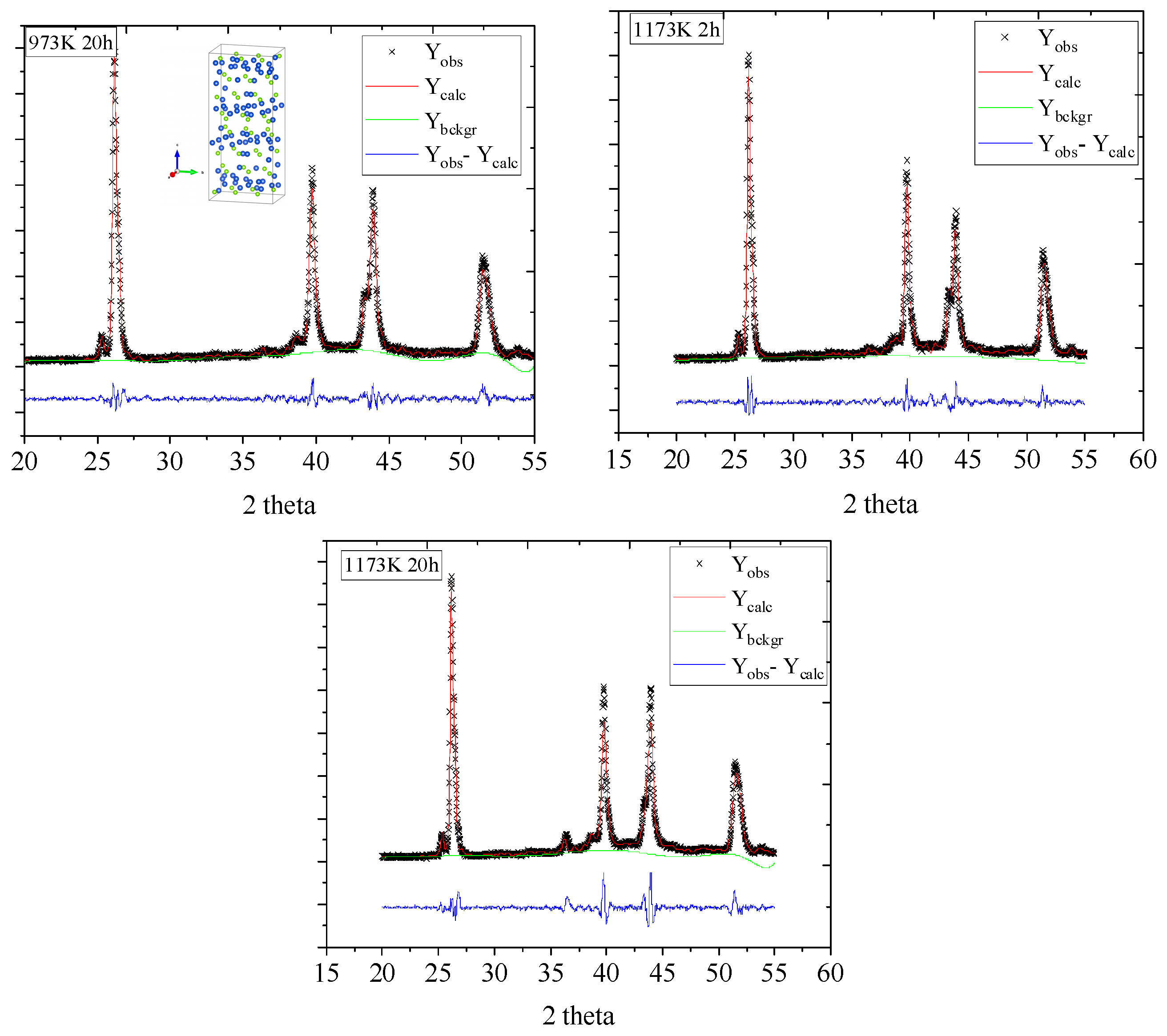
Figure 3.
Scanning electron microscopy (SEM) graphs for the Cu2Se samples sintered under different conditions: (a) 973 K for 20 h; (b) 1173 K for 2 h; (c) 1173 K for 20 h.
Figure 3.
Scanning electron microscopy (SEM) graphs for the Cu2Se samples sintered under different conditions: (a) 973 K for 20 h; (b) 1173 K for 2 h; (c) 1173 K for 20 h.
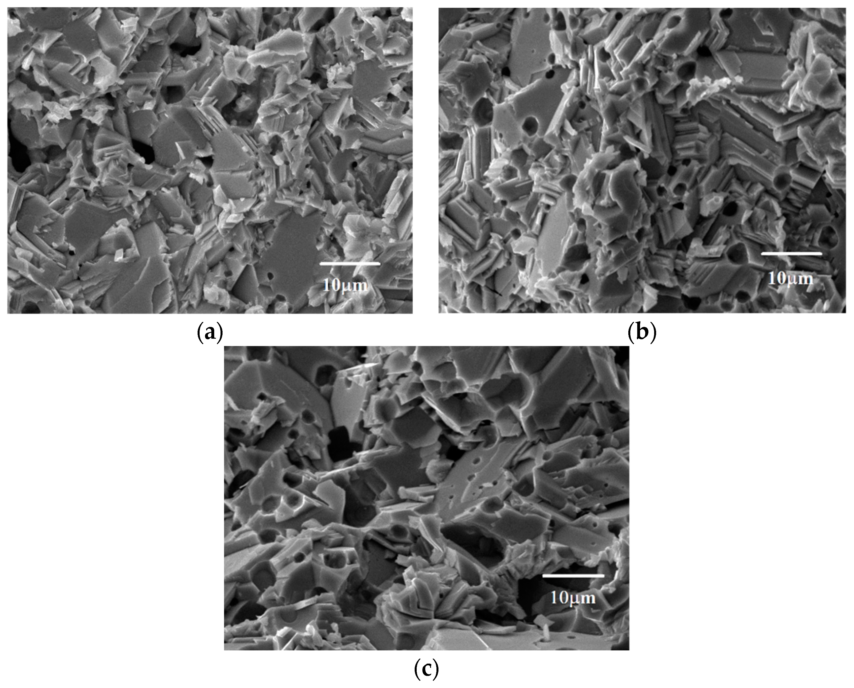
Figure 4.
Thermoelectric properties ((a) electrical conductivity, σ; (b) Seebeck coefficient, S; (c) power factor, PF; and (d) thermal conductivity, κ) for the Cu2Se samples sintered under different conditions.
Figure 4.
Thermoelectric properties ((a) electrical conductivity, σ; (b) Seebeck coefficient, S; (c) power factor, PF; and (d) thermal conductivity, κ) for the Cu2Se samples sintered under different conditions.

Figure 5.
zT values for the Cu2Se samples sintered under different conditions.


Table 1.
The results of the Rietveld analysis of samples.
| Samples | Lattice Parameters | R-Factors | ||||||
|---|---|---|---|---|---|---|---|---|
| a (Å) | b (Å) | c (Å) | beta | Vol (Å3) | χ2 | Rp (%) | Rwp (%) | |
| Cu2Se-973 K 20 h | 7.158 | 12.470 | 27.574 | 94.669 | 2452.977 | 2.535 | 7.09 | 9.34 |
| Cu2Se-1173 K 2 h | 7.110 | 12.505 | 27.391 | 95.165 | 2425.473 | 2.58 | 7.17 | 9.39 |
| Cu2Se-1173 K 20 h | 7.164 | 12.376 | 27.432 | 94.408 | 2424.877 | 4.459 | 9.74 | 12.85 |
© 2019 by the authors. Licensee MDPI, Basel, Switzerland. This article is an open access article distributed under the terms and conditions of the Creative Commons Attribution (CC BY) license (http://creativecommons.org/licenses/by/4.0/).
Share and Cite
MDPI and ACS Style
Shi, D.; Geng, Z.; Lam, K.H. Study of Conventional Sintered Cu2Se Thermoelectric Material. Energies 2019, 12, 401. https://doi.org/10.3390/en12030401
AMA Style
Shi D, Geng Z, Lam KH. Study of Conventional Sintered Cu2Se Thermoelectric Material. Energies. 2019; 12(3):401. https://doi.org/10.3390/en12030401
Chicago/Turabian StyleShi, Dongliang, Zhiming Geng, and Kwok Ho Lam. 2019. "Study of Conventional Sintered Cu2Se Thermoelectric Material" Energies 12, no. 3: 401. https://doi.org/10.3390/en12030401
Note that from the first issue of 2016, this journal uses article numbers instead of page numbers. See further details here.