Partial Discharges in Insulating Systems of Low Voltage Electric Motors Fed by Power Electronics—Twisted-Pair Samples Evaluation


1
ABB Corporate Research Center, ul. Starowislna 13A, 31-216 Krakow, Poland
2
AGH University of Science and Technology, al. Mickiewicza 30, 30-059 Krakow, Poland
*
Author to whom correspondence should be addressed.
Energies 2019, 12(5), 768; https://doi.org/10.3390/en12050768
Submission received: 5 December 2018
/
Revised: 20 February 2019
/
Accepted: 21 February 2019
/
Published: 26 February 2019
(This article belongs to the Section F: Electrical Engineering)
Abstract
:Power electronics switching devices currently represent the dominant technology for supplying low voltage (LV) electric motors. The fast switching processes exert a different class of stress on dielectric insulating materials than standard sinusoidal excitations. Such stresses result in an increase in the dynamic activity of the working electric field, which in turn lead to an increased likelihood of partial discharges (PD). The stator design of low voltage motor is often in form of random-wound windings, where the magnet wires (copper or aluminum round wires coated with thin layer of insulation) form a common system of coils with not precisely defined mutual position of particular turns, resulting in various turn-to-turn and coil-to-coil voltage distributions. Pulse Width Modulated (PWM) voltage waveforms from modern electronic inverters are characterized by very short rise times and presence of repetitively occurring overvoltages that can significantly stress the insulation of feeding cables and motors. These factors influence the inception and dynamics of PD and processes of space charge accumulation in electrical insulation. In this paper investigations performed on round magnet wire twisted-pair samples representing LV motor random-wound winding elements are presented. Special attention was afforded to the twist configurations, observed breakdown voltage and PD activity. To describe the field conditions for the formation of PD in the turn-to-turn insulation system, the results of numerical simulations of electric field distributions for winding wires with different diameters, modeled using the COMSOL program, were analyzed. PD created in the insulating systems of model twisted-pair systems were registered and analyzed using the phase resolved partial discharge analysis (PRPDA) method.
1. Introduction
Power electronics switching devices currently represent the dominant technology for supplying power to new, industry performance low voltage motors. The fast switching processes exert a different class of stress on dielectric insulating materials than standard sinusoidal excitations [1,2]. Such stresses result in an increase in the dynamic activity of the working electric field, which in turn lead to an increased likelihood of partial discharges (PD). In the last decades, the influence of Pulse Width Modulated (PWM) voltages, creating sequences of almost rectangular (semi-square) voltage pulses with very steep slopes and high switching frequencies, generated by modern electronic inverters of variable speed drives (VSDs) with very fast solid-state switches (e.g., IGBT, MOSFET), is a topic which has received considerable attention. PWM voltage waveforms with very fast slopes cause overvoltages with relatively high values, generated due to transmission line phenomena and resonances, that stress insulating systems of feeding cables and motors [1,2,3]. These factors change conditions for processes of space charge accumulation, which influence on initiation and dynamics of PD development in electrical insulating systems [4]. As a result, it leads to acceleration of aging processes and shortening the lifetime of insulation [4,5,6,7].
The stator windings design of low voltage three-phase electric motors for industrial applications (with the rated phase-to-phase voltage Up-p up to 690 V) are usually in form of random-wound windings inserted into the slots [8,9], where the magnet wires (copper or aluminum round wires coated with thin layers of insulation) form a common system of coils with not precisely defined mutual position of particular turns (Figure 1), resulting in various turn-to-turn and coil-to-coil voltage distributions. A basic setup of induction motor controlled by voltage source inverter of VSD is presented in Figure 2. A modulated sequence of almost rectangular voltage pulses, generated by inverter, is fed to terminals of the three-phase motor via a feeding cable (in industrial applications having length up to tens of meters or more), which for fast rising/falling voltage pulses can be treated as a long transmission line. For voltage inverters based on very fast switches, the rise times of voltage pulses can be in the order of 10−10 s, and the voltage slew rate can be significantly greater than 1 kV/µs (i.e., greater than 109 V/s). The accompanying physical phenomena occurring in electrical circuits lead to significant overvoltages and oscillations at the motor terminals and in the cable. The length, characteristic impedance and per unit electrical parameters of the feeding cable have important meaning for working of inverter-cable-motor system, because in many situations can result in unwanted resonances and oscillations [3,7,10,11].
Fast changing voltage at motor terminals causes a change of voltage distribution in the stator winding and leads to an increase in inter-turn voltage in certain parts of the winding, in relation to the distribution at AC 50/60 Hz [12,13]. As result, local voltage increasing may be sufficient for the occurrence of electric field stress initiating of PD activity. Inception of PD, and then their activity in the insulation system depend on a number of factors. In the insulation of the stator windings of LV motors, PD occur in defects that were created in the imperfect production process or during motor operation (mainly due to mechanical, thermal and electrical stresses). In windings impregnated with epoxy resin, discharges can be generated, for example, in gaseous inclusions, but in windings without global impregnation they will develop in the air, in the areas between the wires and on the insulation surface of the wires [14]. Figure 3 presents simplified examples of specific defects, especially PD sources, that can occur in insulating systems of random-wound windings.
For the initiation of electrical discharge, it is necessary to locally exceed the critical value of the electric field strength and the first electron, starting the ionization process, must be available. For this reason, the impact on the occurrence of discharges have: polarity, value and rate of voltage changes, geometry of electrodes (wires) and insulating system, values of electrical permittivity of insulating materials, temperature and pressure of air, humidity, state and electrical properties of dielectric surface, PWM voltage sequence, etc. [10,11,15,16,17,18,19,20]. Impacts of PD, being the basic factor that accelerates aging of magnet wires insulation [4], are increased for PWM voltages due to:
- High repetition rate of PWM voltage pulses with associated overvoltages;
- High steepness of voltage rise;
- Electric charge injection and accumulation processes, dependent not only on the properties of dielectric materials, but also on the time-varying motor control sequences.
Research issues related to the generation and impact of PD on the insulation of magnet wires is very wide. Because the electric field strength between the winding wires and on their surface depends on the diameter of the wires, this aspect must be taken into account when analyzing the conditions for PD initiation. The article presents the results of research on the influence of winding wire diameter and the number of wire twists in twisted-pair samples as well as the steepness of semi-square testing voltage on selected reliability parameters of wires. For time-to-breakdown evaluation accelerated aging test at square-wave voltage with 10 kHz switching frequency was carried out for magnet wires of different diameters. To assess the parameters of the electric field in the insulation system of tested twisted-pairs, they were numerically modeled in the COMSOL program and then the 2D and 3D electric field distributions for wires of different diameters were calculated. The analysis of these distributions supported the interpretation of the results of PD measurements, registered by the phase-resolved method (PRPDA). These PD measurements were performed for samples made of different diameter wires, tested at AC 50 Hz voltage with elevated values of voltage for each subsequent test. Twisted-pairs used during all described tests were prepared as recommended in IEC standards [21,22].
2. Modeling of Turn-to-Turn Insulation of Stator Winding in Laboratory Tests
2.1. Twisted-Pair Sample Preparation
In inverter-fed LV motors, PD can occur at the enameled wires forming stator winding and cause deterioration processes in the insulation. The mechanism of PD in random-wound type windings depends on the placement of wires in the stator slots of electrical machine. For laboratory testing of the round magnet wires the simple models of random-wound winding parts, prepared as standardized twisted-pair (TP) samples [21,22] are usually used. Twisted-pair is made using two enamel coated wires of the same diameter, twisted together during strictly defined mechanical procedure (Figure 4).
Twisted-pairs prepared in a repeatable manner, allow to conduct life-time and breakdown voltage tests of the insulation of directly contacting wires, simulating the turn-to-turn system of the LV motor winding. According to [21] nominal length l of twisted-pair sample is 125 mm, and the normalized number of twists ts depends on diameter of tested wire—from 3 twists for diameters 2.000 mm to 2.500 mm up to 33 twists for diameters 0.100 mm to 0.250 mm. In the twisted-pair sample voltage can be fed from a symmetrical source (positive/negative voltage) or an asymmetrical source (one of the wires in a pair is then grounded and the other energized).
Figure 4 shows a schematic of samples made of enameled wires with a small diameter (Figure 4a) and for wires with a larger diameter (Figure 4b). The wires can be in direct contact or partly there may be a small air gap between them. This distance is depicted in cross sections A and B. In cross section A, the distance between wires w depends on the wire diameter and number of twists ts in a sample.
2.2. Breakdown Voltage in Twisted-Pair Samples with Different Number of Twists Time to Breakdown
The assessment of insulation quality of enameled wires was based on a comparison of the breakdown voltage at sinusoidal voltage for twisted-pair samples containing various numbers of twists ts: 1, 3, 5, 10 and 15, as illustrated in Figure 5. The breakdown voltages UBD for samples 0.3 mm (TP0.3) and 0.8 mm (TP0.8) are shown in Table 1 and Figure 6.
In TP samples with different numbers of twists, the number of contact spots between the twisted wires will be also different. Enameled wires may contain manufacturing defects like: nonhomogeneous insulation thickness and gaseous micro-inclusions in the insulation. These defects are distributed along the wire length. Both have an influence on the breakdown voltage UBD and PD mechanism.
In the investigation on the influence of semi-square voltage rise-time tr on the breakdown voltage UBD of TP samples the high voltage modulator SSV [7] as described in Part 4 was used. The following setup was applied:
- Two values of rise time at f = 50Hz: tr1 = 1 kV/160 µs denoted as SSV1, and tr2 = 1 kV/5.8 µs denoted as SSV2;
- Rise time tr2 at frequency f = 500Hz, tr2 = 1 kV/5.8 µs denoted as SSV3.
The results of breakdown voltage at SSVx and for reference at VSIN50 voltage are shown in Figure 7 and Figure 8.
The following influence of voltage SSV rise-time on breakdown voltage of the TP samples was observed:
- When rise-time tr is shorter, the breakdown voltage is smaller, i.e.,: if tr2 < tr1 then UBD SSVtr2 < UBD SSVtr1;
- Further increase of frequency of voltage SSV will lead to the decrease of breakdown voltage UBD UBD SSVtr2(500 Hz) < UBD SSVtr2(50 Hz);
- Breakdown voltage at SSV is smaller than at sinusoidal voltage: UBD SSV < UBD VSIN50;
- There is a distinct impact of the number of twists ts on the breakdown voltage UBD for ts = 1 ÷ 3, but in the range ts = 10 ÷ 15 this influence is practically negligible, breakdown voltage UBD in the case of ts = 1 is much higher than for ts = 15: UBD SSVts=15 < UBD SSVts=1.
2.3. Evaluation of Time to Breakdown
For wires with different diameters, long-term tests were performed to determine the time to breakdown of polyamide-imide insulation of wires for PWM type voltage. For the tests, six twisted-pair samples were prepared for each wire diameter, with the same insulation. As a test voltage source, a semi-square pulse voltage generator with a voltage of 1 kV and a repetition frequency of 10 kHz was used. In each of the tested twisted-pair one wire was grounded and the test voltage was applied to the other. The analysis of the test results (shown in Figure 9) indicates that during the accelerated aging test, a significantly shorter average life-time has the insulation of wires with a smaller diameter.
3. Numerical Modelling of Electric Field in Twisted-Pair Sample
3.1. Geometry of Twisted-Pair Insulation System
The TP insulation system consists of two layers of enamel covering the wires and the air surrounding the wire (Figure 10a). If the wires do not touch directly, a thin layer of air between them creates an additional serial microgap g (Figure 10b).
- Zone 1 (Figure 10c) is located in the area of the microgap between adjacent winding wires. This area is characterized by a high intensity of the electric field, with the dominant normal component of the field strength, perpendicular to the surface of the wires’ insulation. The field strength in the insulation is significantly smaller than the field strength in the gap due to the difference in the dielectric relative permittivity (εr about 3.8 to 4.2 for used solid insulation).
- Zone 2 (Figure 10c) covers the area between the curvatures of both wires, with the widening area of the air insulation. Due to the geometry of this part of the insulating system, there is also a tangential component present in addition to the normal component of the field on the surface of the wires insulation.
The analysis of electric field strength distribution indicates that the maximum strength values occur in the area adjacent to the winding wires contact point. In this area, therefore, there are potential conditions for PD initiation and development. This fact is confirmed by optical observations of PD during twisted-pair samples tests (Figure 11).
3.2. Simulations of Electric Field in Parallel Configuration of Wires in Twisted Pair Sample
In geometrically simplified, parallel configuration of winding wires without twists (ts = 0) two separated cases can be considered: (1) two wires are directly in contact with each other, microgap g = 0, and (2) two wires are separated by a microgap between them, g > 0. Distributions of electric field strength in the insulation system of a simplified model of a pair of two adjacent wires were numerically modeled using the COMSOL program. During modeling, in all cases (for different wire diameters) it was assumed that the voltage between the wires is 1 kV.
3.2.1. Case 1: Two Wires with Direct Contact
The 2D electric field strength distribution for simplified model of two parallel magnet wires of 0.7 mm diameter, with direct contact (g = 0 mm), is presented in Figure 12. In the figure are marked three selected points with significantly different values of the electric field strength on the surface of the wire insulation. The first point, located near the wires contact point, has a very high field strength value (E > 19 kV/mm). At the second point, slightly distant from the wires contact point, the field strength is still high and is equal to approx. 9.5 kV/mm. The third point determines the place on the surface of the wire insulation, where the field strength decreases below 2 kV/mm.
3.2.2. Case 2: Two Wires with Microgap between Them
The 2D electric field strength distribution for simplified model of two parallel magnet wires of 0.7 mm diameter, with 100 µm air-gap between them, is presented in Figure 13. As previously, for Figure 12, three selected points with significantly different values of the electric field strength on the surface of the wire insulation are marked. The first point, located at the insulation surface area closest to the second wire, has a field strength value exceeding 7 kV/mm. At the second point, located slightly away from the wire approach area, the field strength is still enough high, and is equal to approx. 4 kV/mm. The third point determines the place on the surface of the wire insulation, in which the field strength decreases below 2 kV/mm.
The narrow air-gap between the wires caused a decrease in field strength compared to the state for directly touching wires, however the electric field values on the surface in the area between the wires are still sufficient to initiate PD.
3.3. Electric Field Distribution in Twist Configuration of Magnet Wires Samples
In a real motor winding, the individual turns are twisted, forming quite complex configurations for electric field distribution. As a first approximation of real situation two adjacent turns twisted at the angle α can be considered. The 3D electric potential and electric field distribution in such a setup for α = 45° are illustrated in Figure 14 respectively. The simulation results are obtained for twisted-pair at 50 Hz, and at a voltage of 2 kV. The wire diameter was 0.7 mm, enamel thickness 100 µm, and dielectric relative permittivity was assumed to be εr = 4.2.
3.4. Impact of Wire Insulation Conductivity on Electric Field Distribution in Twisted-Pair Samples
The long-term experiments performed on TP samples show that the partial discharge and PD development process transition through various phases during the insulation degradation process. One can assume that a very high electric field in the zone adjacent to the contact point causes an ionization of the surrounding air-gap along with surface potential decay [23]. While increasing the voltage level, the ionization triangle zone (depicted in red in Figure 15) will enlarge, resulting in an increase of PD inception voltage level. A visualization of this effect, assuming surface conductivity in the triangle boundary area equal to 107 S/m, up to the boundary field level 2 kV/mm, at voltage 1 kV is shown in Figure 16. This effect is also shown graphically in Figure 17, plotting electric field distribution along the white marked cross section depicted in Figure 16b. The left part of the plot corresponds to the ionized zone and the right part represents the air slice without discharges.
4. PD Measurements in Model TP Samples
Quantitative measurements of partial discharges, determined by the apparent charge value of the individual PD pulse, calibrated against the known reference charge value, are performed based on the International Standard IEC 60270 [24]. The PD pulses detection bandwidth is then limited to 1 MHz. This requirement is adequate for PD measurements performed with sinusoidal test voltages with standard network frequencies (50 Hz/60 Hz). In the case of PWM voltages (especially with a very short voltage rise time), standard PD measurements are significantly impeded, and sometimes even impossible to perform reliably, due to strong impulse disturbances. In such situations, alternative methods of detecting PD in VHF/UHF bands are used, without calibration of the apparent charge value [23,25,26,27,28].
Tested twisted-pairs, used for PD acquisition and analysis, were made from enameled copper wires with two significantly different diameters: (1) TP1, diameter 0.67 mm, (2) TP2, diameter 2.24 mm. Both tested samples had the same layered polyamide-imide insulation, thickness 40 μm.
Laboratory tests were carried out using a procedure during which insulation system of each tested twisted-pair was preliminary subjected to square wave voltage stress produced by voltage source with controlled parameters. For example, the programmable voltage source SSV (Figure 18) can generate 6 kV unipolar or ±3 kV bipolar waveforms with pulse rise time within the range of 500 ns to a few μs. The waveform pattern and switching frequency are defined by a programmable arbitrary function generator which delivers a control signal to the inverter. This signal can be the PWM pattern or a simple square wave. The signal from the function generator drives the time control logic module, the function of which is to set the proper delay time between signals that are sent by optical fiber links to the IGBT drivers. This short delay is needed to prevent short circuit of power supply by IGBT modules during switching operation. The IGBT inverter switches DC voltage that is delivered from the power supply according to signal produced by the function generator.
Measurement setup and laboratory equipment used during PD data acquisition at AC voltage are presented in Figure 19 and Figure 20. Partial discharge measurements were carried out on pre-stressed samples using a 50 Hz sinusoidal testing voltage (with a very low value of THD) and a classical PD detection system compliant with IEC 60270 standard. Sets of PD pulses were recorded with the ICMsystem (Power Diagnostix Systems) and processed using MATLAB software, which allows for the collection, comparison and analysis of the differences in PRPD patterns [24,26] of the tested TP samples. The Phase Resolved PD acquisition is well recognized and allows to conduct comparative analyzes, taking into account the apparent charge and the phase of occurrence of individual PD pulses. Digitized raw data of the PD, i.e., the phase of occurrence and the apparent charge are collected by successive accumulation of the number of events (pulses) in a two- dimensional 256x256 elements matrix ϕ-q (which finally leads to the analysis of PD data in the numerical 3D space ϕ-q-n).
Partial discharges for every sample were recorded in 60-second measurement intervals at increasing test voltage; starting from the inception voltage Ui (determined during test as the voltage at which at least one PD pulse occurs statistically in one voltage period). When taking measurements on TP samples, it was found that the Ui value is in the range from about 900 V to about 1000 V, so for each of the TP sample PRPD patterns were recorded for test voltage increasing up to 1600 V. The PRPD patterns shown in Figure 21 and Figure 22 were acquired from TP1 and TP2 samples at four values of testing voltage Umax = 1.0 kV, 1.2 kV, 1.4 kV, and 1.6 kV.
Along with the increase of the testing voltage, in the registered PRPD patterns are clearly noticed two individual data structures D1 and D2 (pointed in Figure 21), associated with two forms of PD appearing in the TP sample insulation system. The reference to the electric field strength distribution in the insulation system of two parallel wires, defining the basic conditions for initiating the PD, allows to analyze the mechanisms leading to the development of two forms of PD indirectly observed in PRPD patterns. In the areas adjacent to the contact point of the wires (Figure 12) or in the microgap (Figure 13), already under the voltages of hundreds of volts, there are electric field conditions enabling PD to occur. Unlike PD generated in closed gaseous inclusions (internal voids), these areas are open sources of PD, in which the energy of discharges dissipated in the form of heat does not cause a progressive change in air pressure. For the test voltage equal to 1 kV (i.e., a bit higher than Ui for TP1 sample), the number and apparent charge (maximum and average) of PDs recorded for the twisted-pair TP1 (Figure 21a) are clearly higher than in the case of the twisted-pair TP2 (Figure 22a). This relation is also maintained for increased values of test voltage.
Using the data contained in the ϕ-q matrix, the amplitude and phase distributions of selected PD parameters were determined (Figure 23). The amplitudes distributions of the number n of PDs for individual values of the apparent charge q were determined by summing up the values of the row elements of the matrix (Figure 23a). The basic phase distribution of the number n of PD in the function of the voltage phase ϕ was determined by summing the values of the matrix column elements (Figure 23b) and the next two (Figure 23c,d) taking into account the values of the apparent charge q.
The analysis of registered PD patterns for gradually increasing test voltage (Figure 21a and Figure 22a; Figure 21b and Figure 22b; Figure 21c and Figure 22c; Figure 21d and Figure 22d) reveals changes in the basic descriptive parameters of PD pattern: total discharge number, maximum charge and phase ranges of PD for positive and negative half-period of test voltage. At the same time, changes in the PD pattern shape are clearly visible, which correspond to the ‘turtle’ like and ‘rabbit-ear’ like patterns observed for measurement data registered for gaseous void in solid dielectric [29]. The appearance of the D2 group in the PD pattern is associated with the presence of surface discharges, developing with increasing value of testing voltage, together with processes of charge accumulation and changes of the surface conductivity of the enamel (Figure 16). The presence of the electric field tangent component on the wire insulation surface (demonstrated in numerical simulations) affects the development of these form of PD.
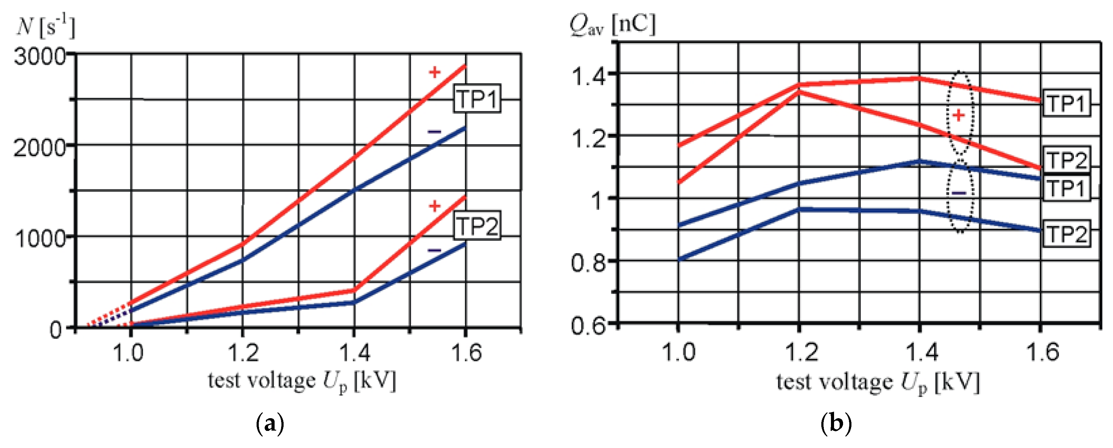
Two forms of PD also manifest their presence in the amplitude and phase distributions of PD pulses (Figure 23). The parallel occurrence of these discharges causes that these distributions are the sum of two individual distributions for form D1 and D2. The PD phase distributions n(ϕ) (Figure 23c,d) and Σq(ϕ) (Figure 23e,f) reveal that PDs are present in two voltage half-cycles up to voltage peaks and that along with the increasing test voltage value the PD phase range widens as a result of decreasing the phase angle of PD inception. The analysis of the phase distributions of the average charge Qav(ϕ) (Figure 23g,h) confirm the observation made for PRPD patterns (Figure 21 and Figure 22), that the surface discharges (form D2) are characterized by a higher values of the charges, both the maximum and the average. Analysis of the dependence of the number of PD per second N vs. test voltage, reveals the over-linear increase in the number of discharges with increasing voltage (Figure 24a). This global statistical parameter has a much higher value for a TP samples made of wire with a smaller diameter. The greater repetition rate of discharges (Figure 24a) and the larger value of the average apparent charge Qav (Figure 24b) means a higher level of aging exposure to which the enamel insulation of thinner wires is subjected, at the same test voltage value. Along with the increase of the test voltage, the average apparent charge Qav initially increases - caused by a larger charge of surface discharges, and then its lowering (Figure 24b), which is associated with a significant increase in the number of D1 discharges, with a relatively small apparent charge (Figure 21d, Figure 22d and Figure 23a,b).
5. Conclusions
Modern electric drives use control systems based on power electronics converters producing PWM voltages with short rise times and high repetition frequencies. Since the 1990s, the problem of shortening the lifetime of electric motors insulation has been recognized, however, due to the requirements for increasing the reliability of electrical equipment, it remains an up-to-date research problem. The paper presents selected aspects of research on the impact of repetitive, fast-changing voltages on the insulation of winding wires with polyamide-imide insulation. The test objects were twisted-pairs made of magnet wires of various diameters, according to a standardized procedure, however with a variable number of turns. Laboratory tests were performed using both 50 Hz sinusoidal voltage and semi-square voltages with different voltage rise times and different repetition frequencies. The conclusions resulting from the research can be divided into several groups.
Accelerated aging of magnet wire insulation is caused primarily by the occurrence of PD. Due to overvoltages generated in the induction motor supplying systems and high repetition frequency of the PWM voltage pulses, the intensity of the PD can be very large even in the stator windings of the low voltage motors (Up-p < 1 kV). They cause progressive degradation of the insulating enamel layers and, as a result, lead to insulation breakdown.
The results of the tests performed on the TP samples indicate that the number of turns is of significance for the test results. To obtain the possibility of comparing the results performed at different time and on different wires, it is always necessary to use one, the same number of turns for wires of the same diameter (number of twists specified in the standard), with the same procedure of sample preparation.
The breakdown voltage of TP samples with identical wire insulation depends both on the diameter of the wire and the number of turns made as well as on the type of voltage, sinusoidal or semi-square. For the second type of voltage, the pulse repetition frequency and impulse voltage steepness have a fundamental influence on the test results.
Due to the field nature of stresses leading to the formation of PD in insulation systems, for windings working at the same voltage, windings with wires of smaller diameter can be more exposed to the initiation and development of PD.
Simulations of electric field distributions in a model system of two neighboring magnet wires and laboratory measurements of PD on twisted pairs with wires of different diameters indicate the development of two PD forms in such a wire configuration. Simultaneously with PD arising in air near the point of contact of wires or in the microgap between them (corona discharges), under certain conditions also surface PD are generated, characterized by higher values of the maximum charge. Both forms of discharges build clearly separated PD patterns in the ϕ-q-n space, created on the basis of data from measurements at AC voltage. The impact on these forms of PD has a number of factors, including charge accumulation processes, surface conductivity of the enamel insulation and specific field distribution in the area near the magnet wires contact point. The analysis of amplitude and phase distributions (Figure 23) allowed to determine the properties of selected PD parameters sensitive to the test voltage value and wire diameter, e.g., number of PD pulses per second N (Figure 24a) or the average apparent charge Qav (Figure 24b).
An important direction of research in the field of magnet wire insulation is currently the application of modified nanocomposite materials [30,31,32,33]. The presented research conclusions remain valid, including the influence of wires and twisted-pair samples geometry as well as the method of their preparation on test results, also for tests of new types of insulation with higher resistance to PD.
Author Contributions
The authors cooperated fully and equally at all stages of the presented research and during the preparation of the article.
Funding
Researches were partially funded by Polish National Science Center (NCN) grant NR 01 0019 04.
Conflicts of Interest
The authors declare no conflicts of interest.
References
- Bonnett, A.H. Analysis of the impact of pulse-width modulated inverter voltage waveforms on AC induction motors. IEEE Trans. Ind. Appl. 1996, 32, 386–392. [Google Scholar] [CrossRef]
- Weijun, Y. Failure mechanism of winding insulations in inverter-fed motors. IEEE Electr. Insul. Mag. 1997, 13, 18–23. [Google Scholar] [CrossRef]
- Kerkman, R.J.; Leggate, D.; Skibinski, G. Interaction of drive modulation and cable parameters on AC motor transients. IEEE Trans. Ind. Appl. 1997, 33, 722–731. [Google Scholar] [CrossRef]
- Fabiani, D.; Montanari, G.C.; Cavallini, A.; Mazzanti, G. Relation between space charge accumulation and partial discharge activity in enameled wires under PWM-like voltage waveforms. IEEE Trans. Dielectr. Electr. Insul. 2004, 11, 393–405. [Google Scholar] [CrossRef]
- Lebey, T.; Castelan, P.; Montanari, G.C.; Ghinello, I. Influence of PWM-type voltage waveforms on reliability of machine insulation system. In Proceedings of the 8th International Conference on Harmonics and Quality of Power, Athens, Greece, 14–16 October 1998; Volume 2, pp. 994–998. [Google Scholar]
- Grzybowski, S.; Shrestha, P.; Cao, L. Electrical aging phenomena of XLPE and EPR cable insulation energized by switching impulses. In Proceedings of the 2008 International Conference on High Voltage Engineering and Application, Chongqing, China, 9–12 November 2008; pp. 422–425. [Google Scholar] [CrossRef]
- Florkowska, B.; Florkowski, M.; Furgał, J.; Roehrich, J.; Zydron, P. Impact of Fast Transient Phenomena on Electrical Insulation Systems; Publishing House AGH: Kraków, Poland, 2012; ISBN 978-83-7464-480-8. [Google Scholar]
- Wheeler, J.C.G. Effects of converter pulses on the electrical insulation in low and medium voltage motors. IEEE Elect. Insul. Mag. 2005, 21, 22–29. [Google Scholar] [CrossRef]
- Stone, G.C.; Culbert, I.; Boulter, E.A.; Dhirani, H. Electrical Insulation for Rotating Machines: Design, Evaluation, Aging, Testing, and Repair, 2nd ed.; IEEE Press - John Wiley & Sons Inc.: Hoboken, NJ, USA, 2014; ISBN 978-1-118-05706-3. [Google Scholar]
- Hayakawa, N.; Okubo, H. Partial discharge characteristics of inverter-fed motor coil samples under ac and surge voltage conditions. IEEE Electr. Insul. Mag. 2005, 21, 5–10. [Google Scholar] [CrossRef]
- Melfi, M.; Sung, J.; Bell, S.; Skibinski, G. Effect of surge voltage risetime on the insulation of low-voltage machines fed by PWM converters. IEEE Trans. Ind. Appl. 1998, 34, 766–775. [Google Scholar] [CrossRef]
- Florkowski, M.; Furgał, J. High Frequency Methods for Condition Assessment of Transformers and Electrical Machines; Publishing House AGH: Kraków, Poland, 2013; ISBN 978-83-7464-614-7. [Google Scholar]
- Oyegoke, B. Voltage distribution in the stator winding of an induction motor following a voltage surge. Electr. Eng. 2000, 82, 199–205. [Google Scholar] [CrossRef]
- Florkowska, B.; Zydron, P.; Florkowski, M. Effects of inverter pulses on the electrical insulation system of motors. In Proceedings of the 2011 IEEE International Symposium on Industrial Electronics, Gdansk, Poland, 27–30 June 2011; pp. 573–578. [Google Scholar] [CrossRef]
- Lindell, E.; Bengtsson, T.; Blennow, J.; Gubanski, S.M. Influence of rise time on partial discharge extinction voltage at semi-square voltage waveforms. IEEE Trans. Dielectr. Electr. Insul. 2010, 17, 141–148. [Google Scholar] [CrossRef]
- Kikuchi, Y.; Murata, T.; Fukumoto, N.; Nagata, M.; Wakimoto, Y.; Yoshimitsu, T. Investigation of partial discharge with twisted enameled wires in atmospheric humid air by optical emission spectroscopy. IEEE Trans. Dielectr. Electr. Insul. 2010, 17, 839–845. [Google Scholar] [CrossRef]
- Yanaze, N.; Nakaya, H.; Kozako, M.; Hikita, M.; Tomizawa, K.; Ohya, M. Partial discharge inception voltage measurement and location identification of enamel coating ribbon wire used for low-voltage motors. In Proceedings of the 2014 IEEE Conference on Electrical Insulation and Dielectric Phenomena (CEIDP), Des Moines, IA, USA, 19–22 October 2014; pp. 192–195. [Google Scholar] [CrossRef]
- Guastavino, F.; Ratto, A.; Dardano, A.; Torello, E.; Biondi, G.; Loggi, G.; Ceci, A. Comparison among the PD resistance behavior of different enameled wires when subjected to PWM voltage. In Proceedings of the 2011 Annual Report Conference on Electrical Insulation and Dielectric Phenomena, Cancun, Mexico, 16–19 October 2011; pp. 314–317. [Google Scholar] [CrossRef]
- Florkowski, M.; Florkowska, B.; Roehrich, J.; and Zydron, P. Measurement and analysis of surface partial discharges at semi-square voltage waveforms. IEEE Trans. Dielectr. Electr. Insul. 2011, 18, 990–996. [Google Scholar] [CrossRef]
- Wang, P.; Xu, H.; Wang, J.; Wang, W.; Cavallini, A. Effect of repetitive impulsive voltage duty cycle on partial discharge features and insulation endurance of enameled wires for inverter-fed low voltage machines. IEEE Trans. Dielectr. Electr. Insul. 2017, 24, 2123–2131. [Google Scholar] [CrossRef]
- IEC 60851-5:2008+AMD1:2011 CSV, Winding Wires—Test Methods—Part 5: Electrical Properties; IEC: Geneva, Switzerland, 2011.
- IEC 60172, Test Procedure for the Determination of the Temperature Index of Enamelled Winding Wires; IEC: Geneva, Switzerland, 2015.
- Hoang, A.T.; Serdyuk, Y.V.; Gubanski, S.M. Mechanisms of surface potential decay on enamel wire coatings. IEEE Trans. Dielectr. Electr. Insul. 2015, 22, 3470–3480. [Google Scholar] [CrossRef]
- IEC 60270:2000+AMD1:2015 CSV, High-Voltage Test Techniques—Partial Discharge Measurements; IEC: Geneva, Switzerland, 2015.
- IEC TS 61934, Electrical Insulating Materials and Systems—Electrical Measurement of Partial Discharges (PD) under Short Rise Time and Repetitive Voltage Impulses; IEC: Geneva, Switzerland, 2011.
- Florkowski, M.; Florkowska, B.; Furgał, J.; Zydron, P. Impact of high voltage harmonics on interpretation of partial discharge patterns. IEEE Trans. Dielectr. Electr. Insul. 2013, 20, 2009–2016. [Google Scholar] [CrossRef]
- Florkowski, M.; Florkowska, B.; Zydron, P. Chopped Partial Discharge Sequence. IEEE Trans. Dielectr. Electr. Insul. 2015, 22, 3451–3458. [Google Scholar] [CrossRef]
- Wang, P.; Cavallini, A.; Montanari, G.C.; Wu, G. Effect of rise time on PD pulse features under repetitive square wave voltages. IEEE Trans. Dielectr. Electr. Insul. 2013, 20, 245–254. [Google Scholar] [CrossRef]
- Illias, H.; Chen, G.; Lewin, P.L. Partial discharge behavior within a spherical cavity in a solid dielectric material as a function of frequency and amplitude of the applied voltage. IEEE Trans. Dielectr. Electr. Insul. 2011, 18, 432–443. [Google Scholar] [CrossRef]
- Kikuchi, H.; Hanawa, H. Inverter surge resistant enameled wire with nanocomposite insulating material. IEEE Trans. Dielectr. Electr. Insul. 2012, 19, 99–106. [Google Scholar] [CrossRef]
- Guastavino, F.; Ratto, A.; Torello, E.; Biondi, G. Aging tests on nanostructured enamels for winding wire insulation. IEEE Trans. Ind. Electron. 2014, 61, 5550–5557. [Google Scholar] [CrossRef]
- Yoo, J.; Kim, Y.; Kwon, S.; Lee, J.; Seo, Y.-S. Surge-resistant nanocomposite enameled wire using silica nanoparticles with binary chemical compositions on the surface. J. Nanomater. 2015, 231672. [Google Scholar] [CrossRef]
- Guastavino, F.; Torello, E.; Cordano, D.; Della Giovanna, L. Surface PD evolution of conventional and nanocomposite enamels. In Proceedings of the 2016 IEEE International Conference on Dielectrics (ICD), Montpellier, France, 3–7 July 2016; pp. 760–763. [Google Scholar] [CrossRef]
Figure 1.
Stator of induction motor with random-wound windings inserted into the slots.

Figure 2.
A basic setup of induction motor connected to voltage source inverter by feeding cable: R, L, C, G—π-section parameters of cable phase, Ld—inductance of winding, Cg—distributed ground capacitance, Re—resistance representing losses, K—input winding capacitance; UDC—inverter DC-link voltage, Uov—maximum value of overvoltage at motor terminal, du/dt—slew rate of impulse voltage, tr—voltage pulse rise time, tf—voltage pulse fall time.
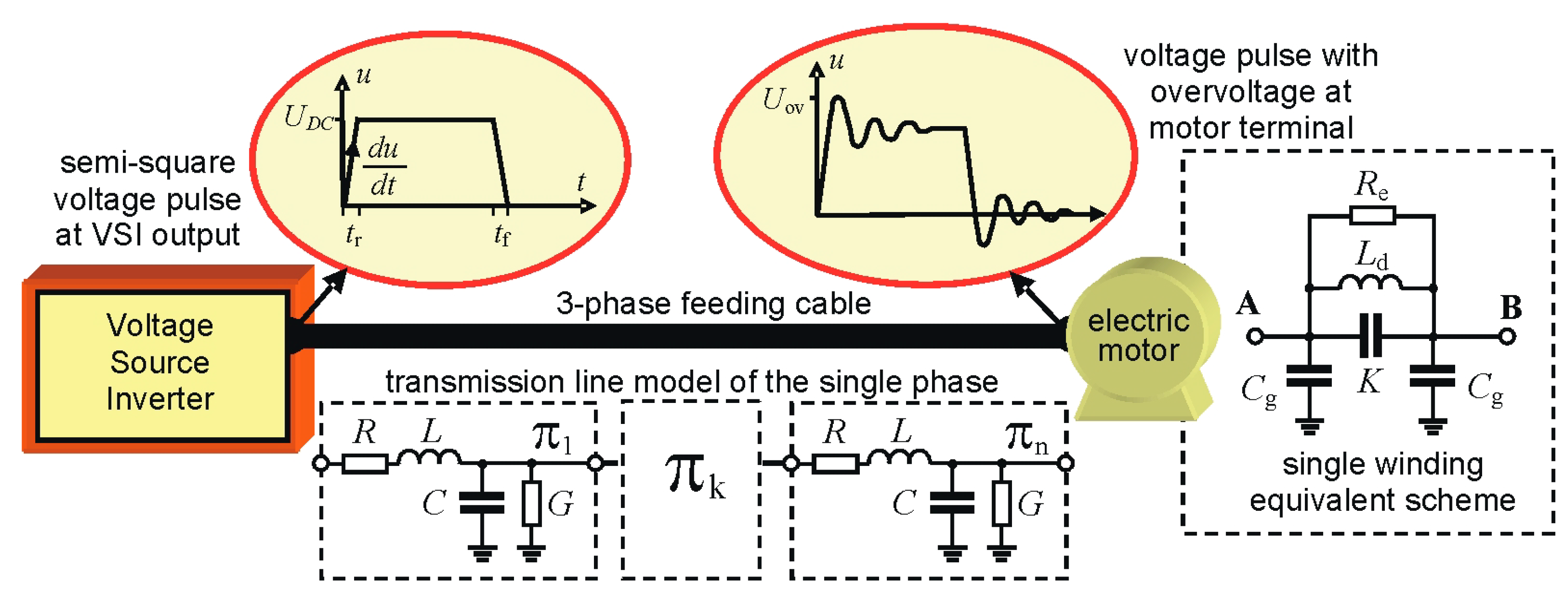
Figure 3.
Specific defects of random-wound windings insulating systems: (a) turns short-circuit, (b) gaseous void between or adjacent to winding wires, (c) and (d) corona or surface discharges at contacting wires in air.
Figure 3.
Specific defects of random-wound windings insulating systems: (a) turns short-circuit, (b) gaseous void between or adjacent to winding wires, (c) and (d) corona or surface discharges at contacting wires in air.
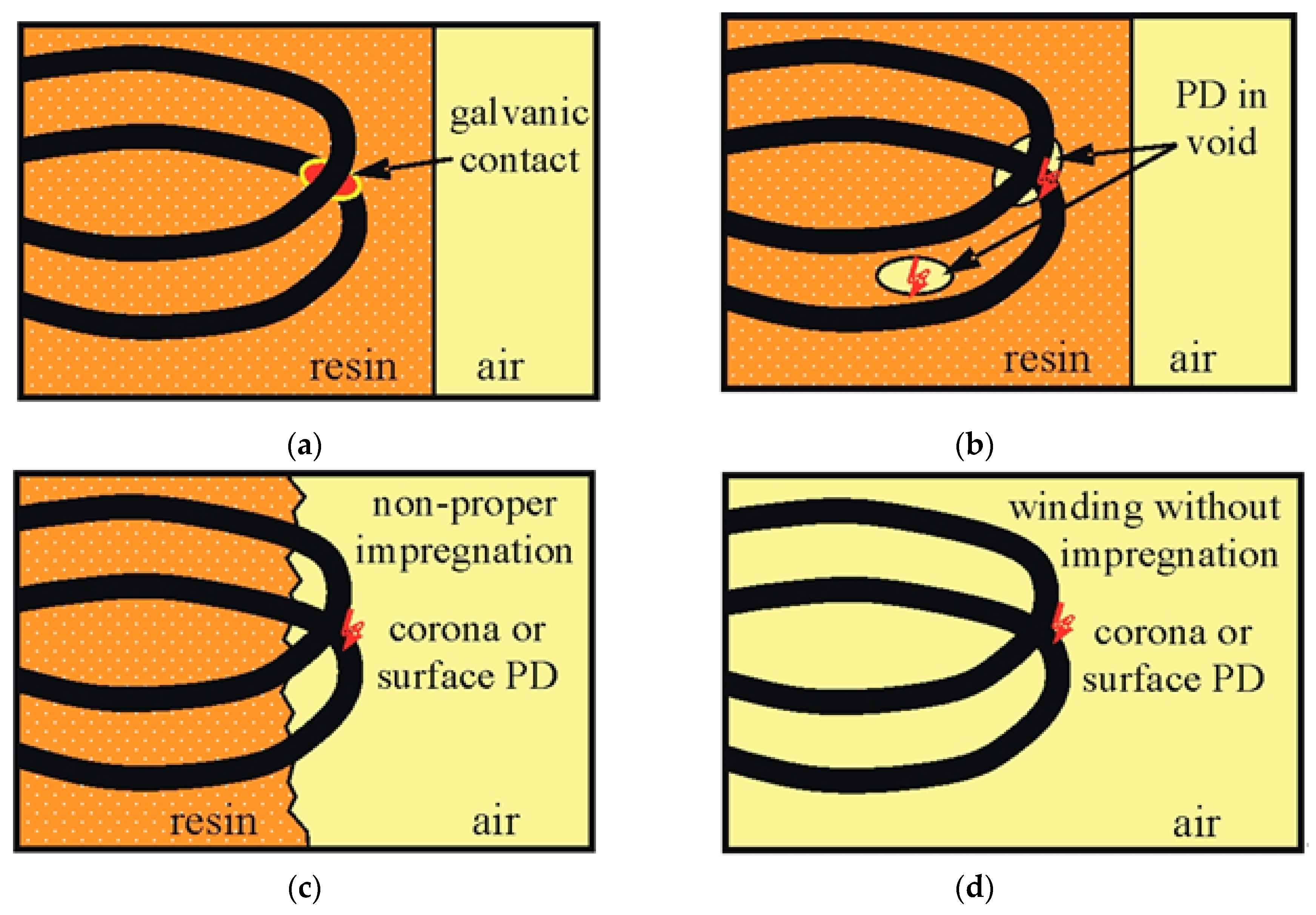
Figure 4.
Part of twisted-pair (TP) sample: (a) small diameter wires; (b) large diameter wires; g—distance between wires in cross section A or B.
Figure 4.
Part of twisted-pair (TP) sample: (a) small diameter wires; (b) large diameter wires; g—distance between wires in cross section A or B.

Figure 5.
Twisted-pair samples with various number of twists ts.

Figure 6.
The dependence of breakdown voltage UBD on the number of twists ts in samples TP 0.3 and TP 0.8 at AC test voltage.
Figure 6.
The dependence of breakdown voltage UBD on the number of twists ts in samples TP 0.3 and TP 0.8 at AC test voltage.
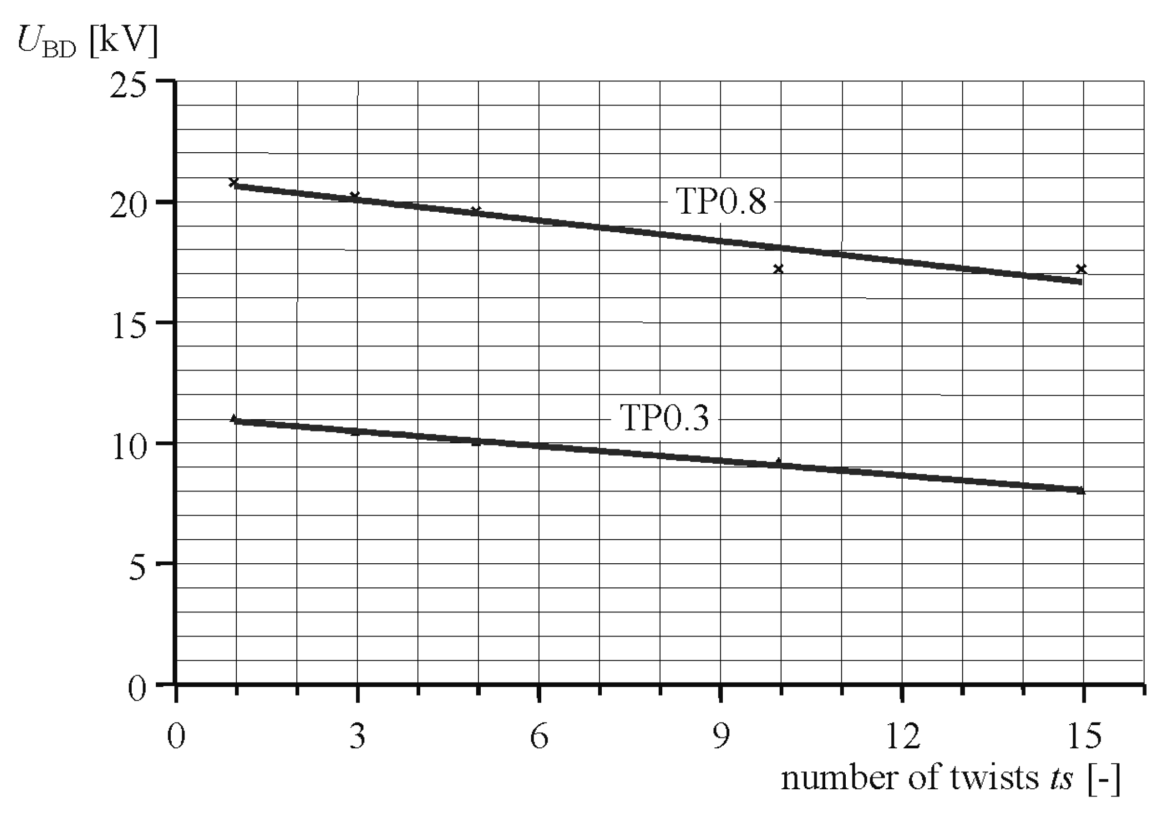
Figure 7.
The dependence of breakdown voltage UBD of TP0.3C samples on number of twists ts at semi-square voltage SSV with rise time: (1) tr1, 50 Hz, (2) tr2 50 Hz, (3) tr2 500 Hz and (4) voltage VSIN50.
Figure 7.
The dependence of breakdown voltage UBD of TP0.3C samples on number of twists ts at semi-square voltage SSV with rise time: (1) tr1, 50 Hz, (2) tr2 50 Hz, (3) tr2 500 Hz and (4) voltage VSIN50.
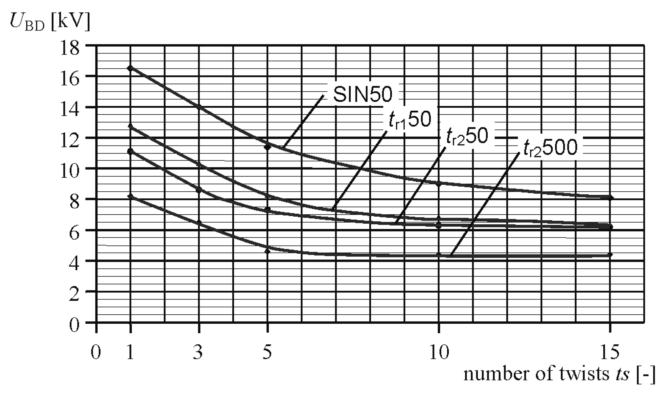
Figure 8.
The dependence of breakdown voltage UBD of TP0.8CC samples on number of twists ts at semi-square voltage SSV with rise time: tr1, (1) 50 Hz, (2) tr2 50 Hz, (3) tr2 500 Hz and (4) voltage VSIN50.
Figure 8.
The dependence of breakdown voltage UBD of TP0.8CC samples on number of twists ts at semi-square voltage SSV with rise time: tr1, (1) 50 Hz, (2) tr2 50 Hz, (3) tr2 500 Hz and (4) voltage VSIN50.
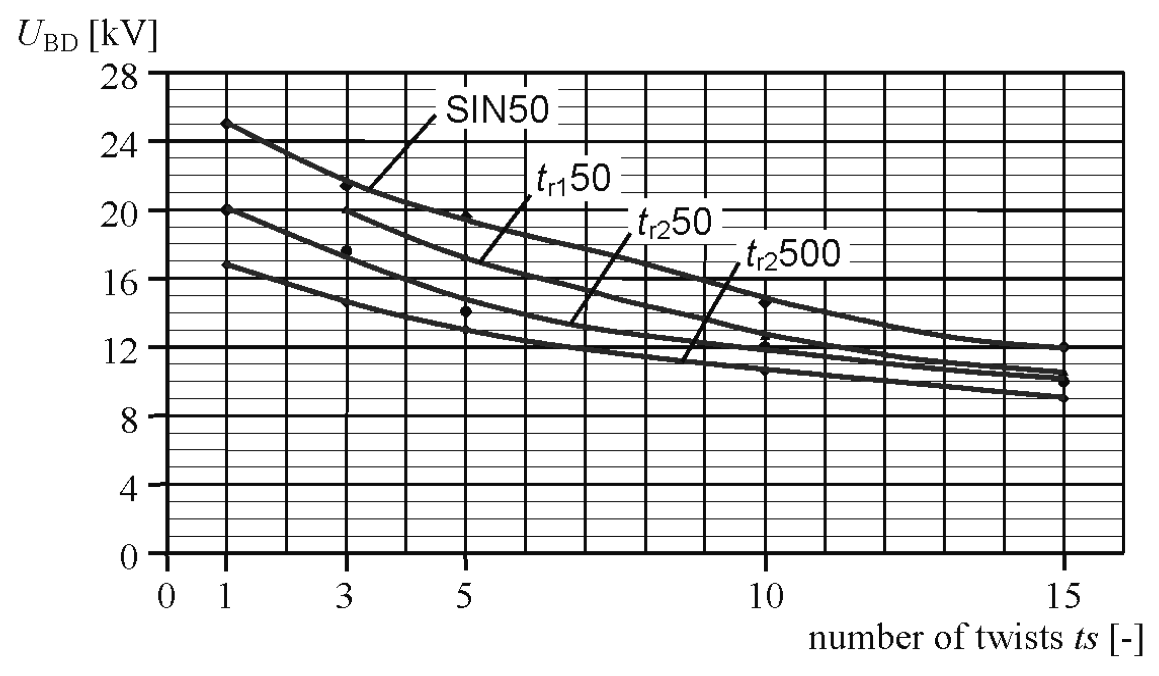
Figure 9.
Influence of magnet wire diameter dw on time-to-breakdown tb for the same testing voltage.
Figure 9.
Influence of magnet wire diameter dw on time-to-breakdown tb for the same testing voltage.

Figure 10.
Simplified geometry of the possible mutual position of two magnet wires in a TP sample (without maintaining the scale of insulation thickness in relation to wire diameter): (a) microgap g = 0; (b) microgap g > 0; (c) location of specific zones in the insulation of adjacent winding wires.
Figure 10.
Simplified geometry of the possible mutual position of two magnet wires in a TP sample (without maintaining the scale of insulation thickness in relation to wire diameter): (a) microgap g = 0; (b) microgap g > 0; (c) location of specific zones in the insulation of adjacent winding wires.

Figure 11.
Example of optical PD observation by high sensitivity camera in TP sample during AC test.
Figure 11.
Example of optical PD observation by high sensitivity camera in TP sample during AC test.
Figure 12.
The 2D electric field strength distribution for two parallel wires with direct contact.
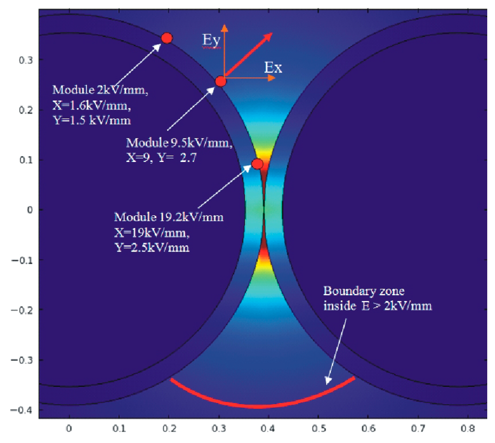
Figure 13.
The 2D electric field strength distribution for two parallel wires with 100 µm air-gap.

Figure 14.
The 3D electric potential (a) and electric field strength (b) distribution in twisted-pair with wire diameter 0.7 mm, for α = 45°, at 2 kV.
Figure 14.
The 3D electric potential (a) and electric field strength (b) distribution in twisted-pair with wire diameter 0.7 mm, for α = 45°, at 2 kV.

Figure 15.
Visualization of the ionization zone and variable surface conductivity area.

Figure 16.
Impact of ionization (triangle zone) on potential distribution (a) and electric field (b).
Figure 16.
Impact of ionization (triangle zone) on potential distribution (a) and electric field (b).

Figure 17.
The electric field strength distribution in the cross-section depicted in Figure 16b.
Figure 17.
The electric field strength distribution in the cross-section depicted in Figure 16b.
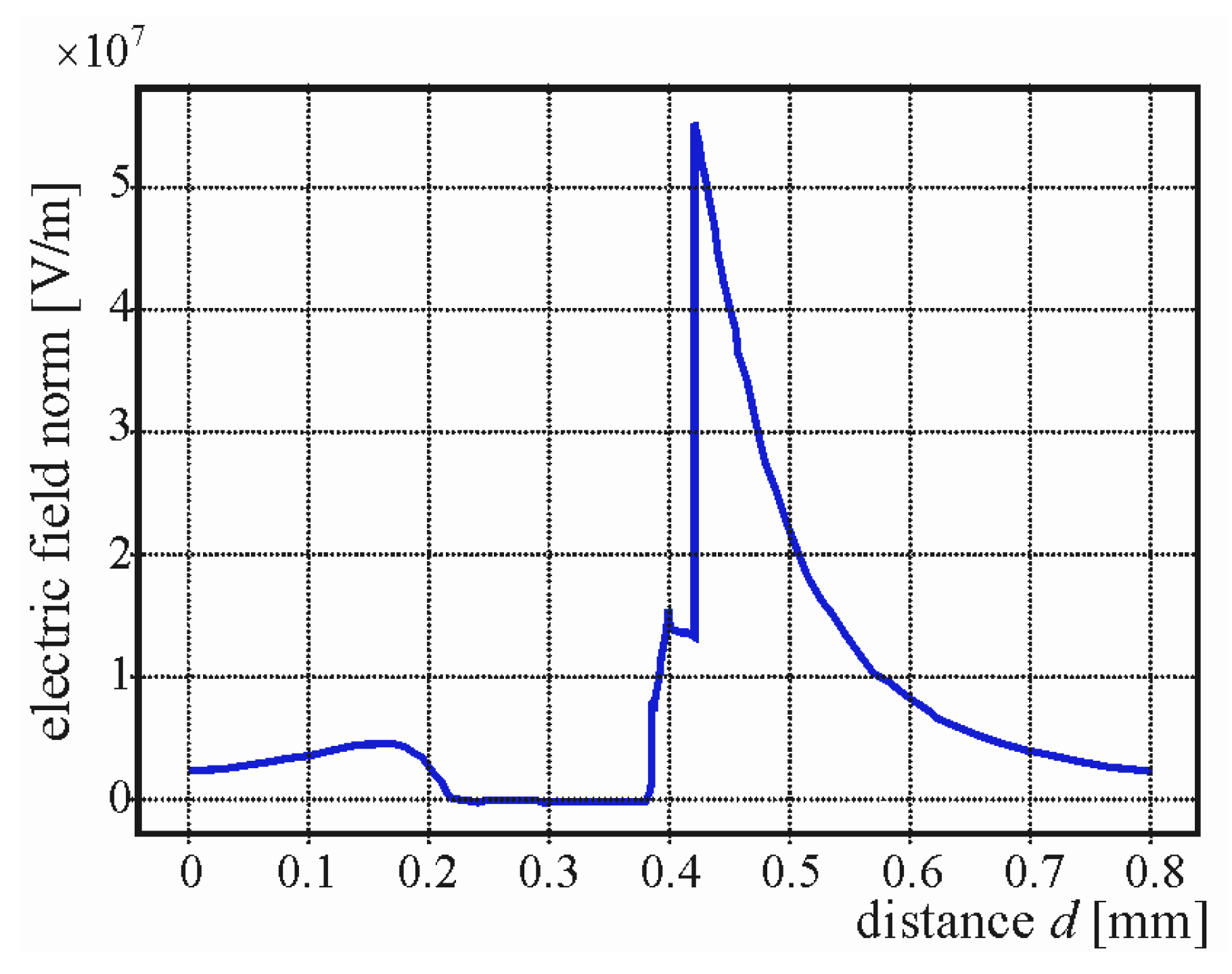
Figure 18.
Block diagram of IGBT modules-based pulse voltage generator (6 kV/±3 kV).
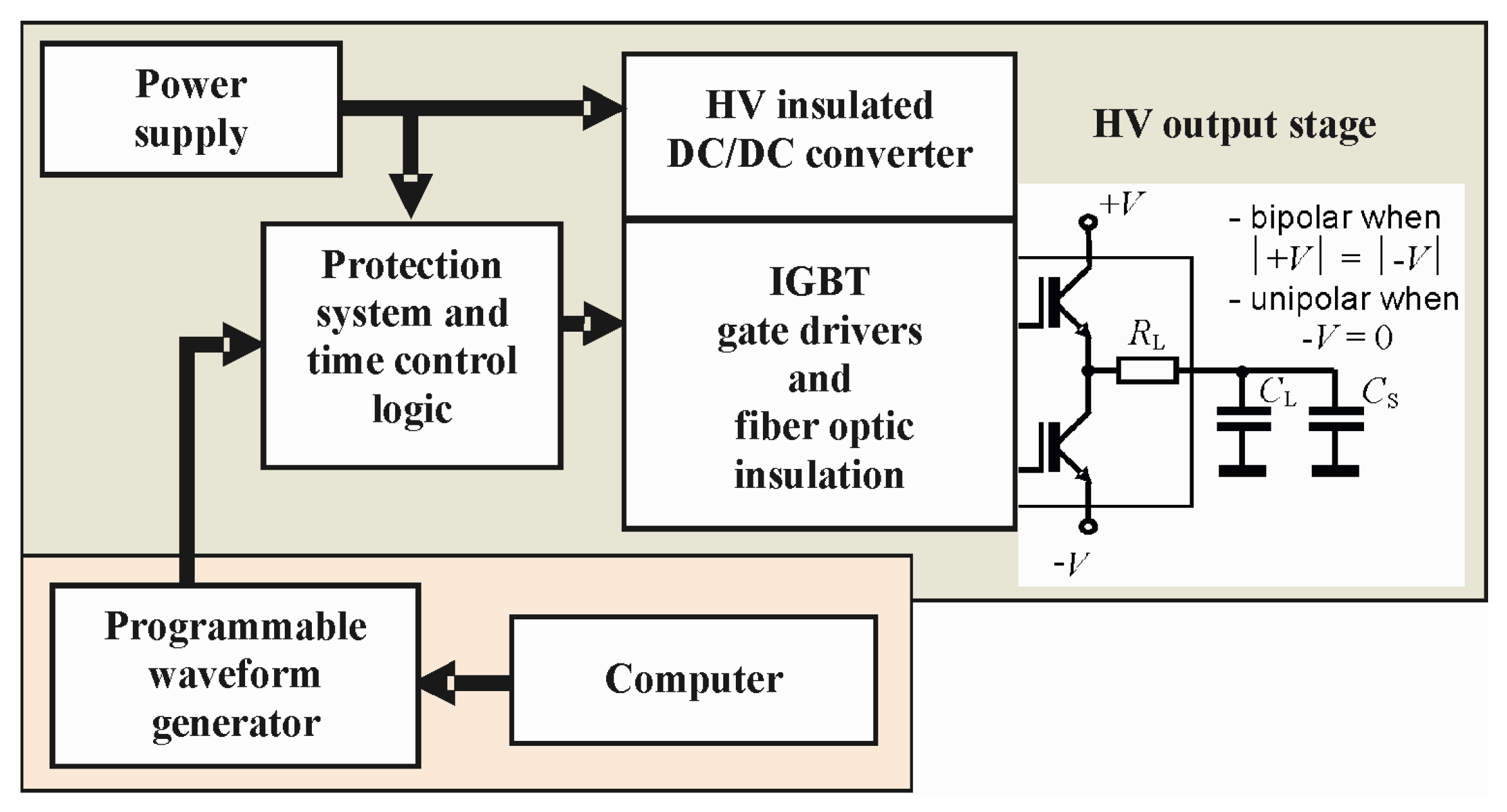
Figure 19.
General block diagram of the laboratory system used for PRPD data acquisition: AWG—arbitrary waveform generator, HVA—high-voltage amplifier, SCU—signal conditioning unit, PDA—PD Analyser, GPIB—IEEE.488 interface, CT—capacitance of tested object, Ck—coupling capacitor, Zm—measuring impedance, R1/R2—HV divider, Zf—impedance of HV filter.
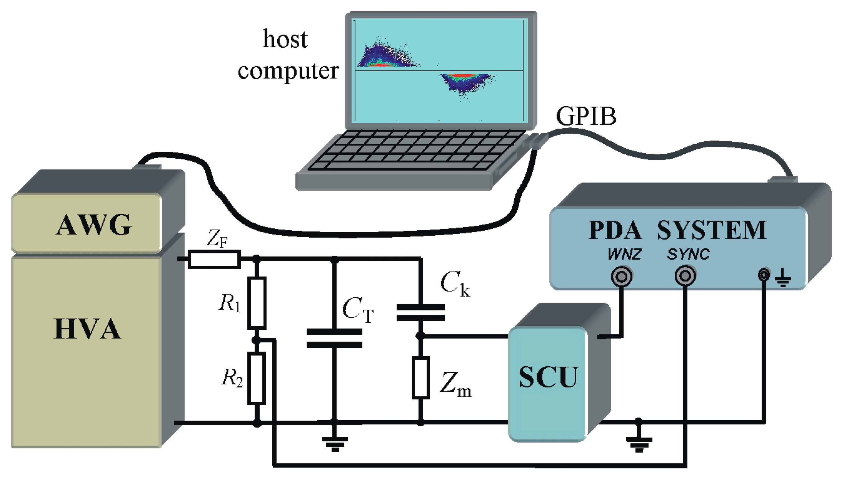
Figure 20.
Laboratory equipment and instruments used for PD measurements: (1) solid-state high- voltage amplifier TREK 20/20B (HVA); (2) arbitrary waveform generator Analogic 2030 (AWG); (3) PD data acquisition system ICMsystem (PDA) with pre-amplifier (SCU); (4) programmable amplifier SR560; (5) digital storage oscilloscope; (6) computer with IEEE.488 interface and control software; (7) electrostatic kilovoltmeter; (8) coupling capacitor Ck; (9) measuring impedance Zm.
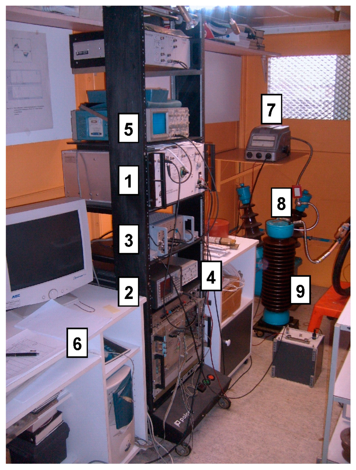
Figure 21.
The PRPD patterns acquired for TP1 sample at four test voltage values: (a) Umax = 1.0 kV; (b) Umax = 1.2 kV; (c) Umax = 1.4 kV; (d) Umax = 1.6 kV.
Figure 21.
The PRPD patterns acquired for TP1 sample at four test voltage values: (a) Umax = 1.0 kV; (b) Umax = 1.2 kV; (c) Umax = 1.4 kV; (d) Umax = 1.6 kV.

Figure 22.
The PRPD patterns acquired for TP2 sample at four test voltage values: (a) Umax = 1.0 kV; (b) Umax = 1.2 kV; (c) Umax = 1.4 kV; (d) Umax = 1.6 kV.
Figure 22.
The PRPD patterns acquired for TP2 sample at four test voltage values: (a) Umax = 1.0 kV; (b) Umax = 1.2 kV; (c) Umax = 1.4 kV; (d) Umax = 1.6 kV.
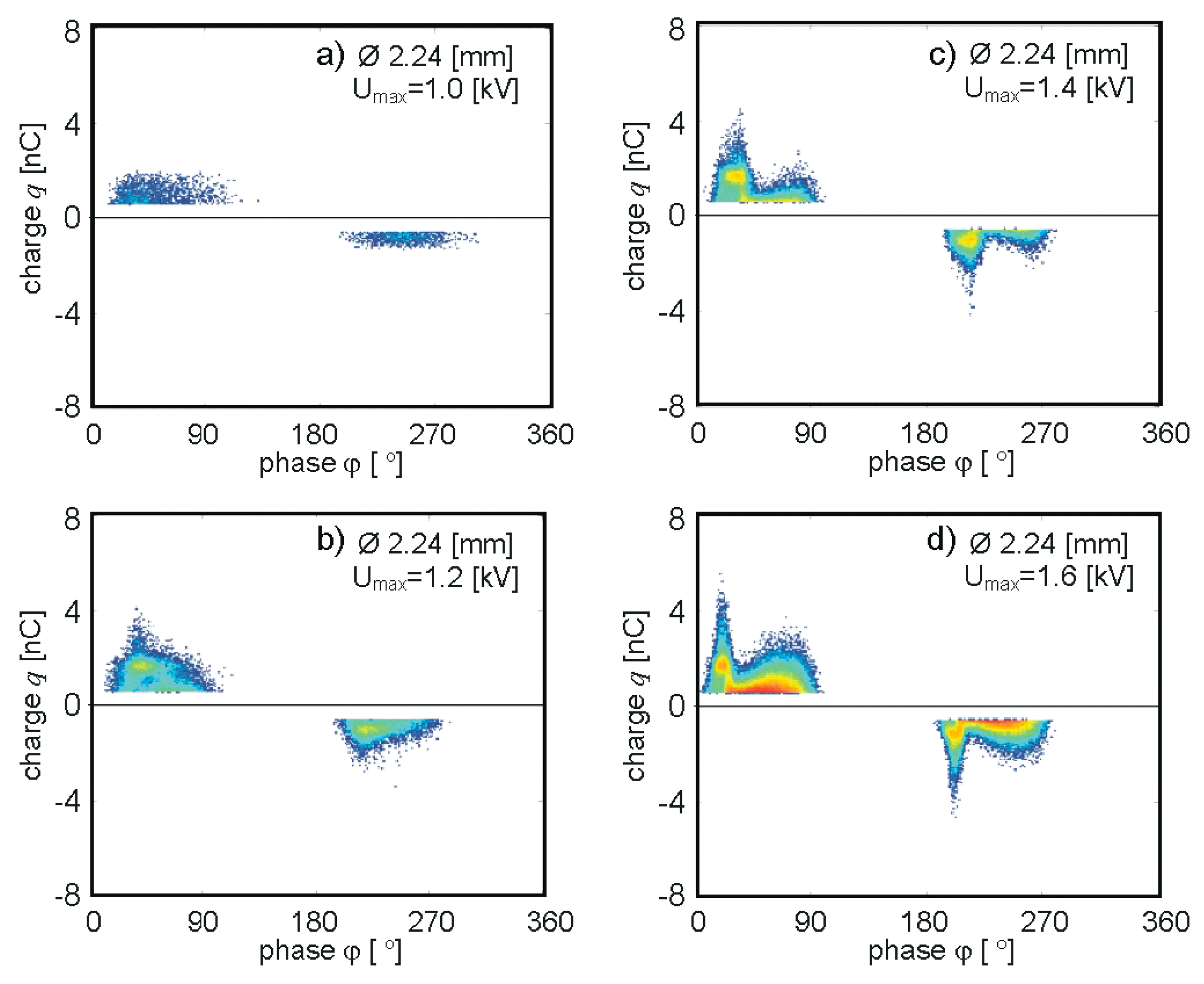
Figure 23.
Evaluated amplitude and phase distributions of PD data for TP1 and TP2 samples: (a) and (b) number of PD pulses vs. apparent charge n(q); (c) and (d) phase distribution of the number of PD pulses n(ϕ); (e) and (f) phase distribution of the total charge Σq(ϕ); (g) and (h) phase distribution of the average charge Qav(ϕ). All data normalized per second.
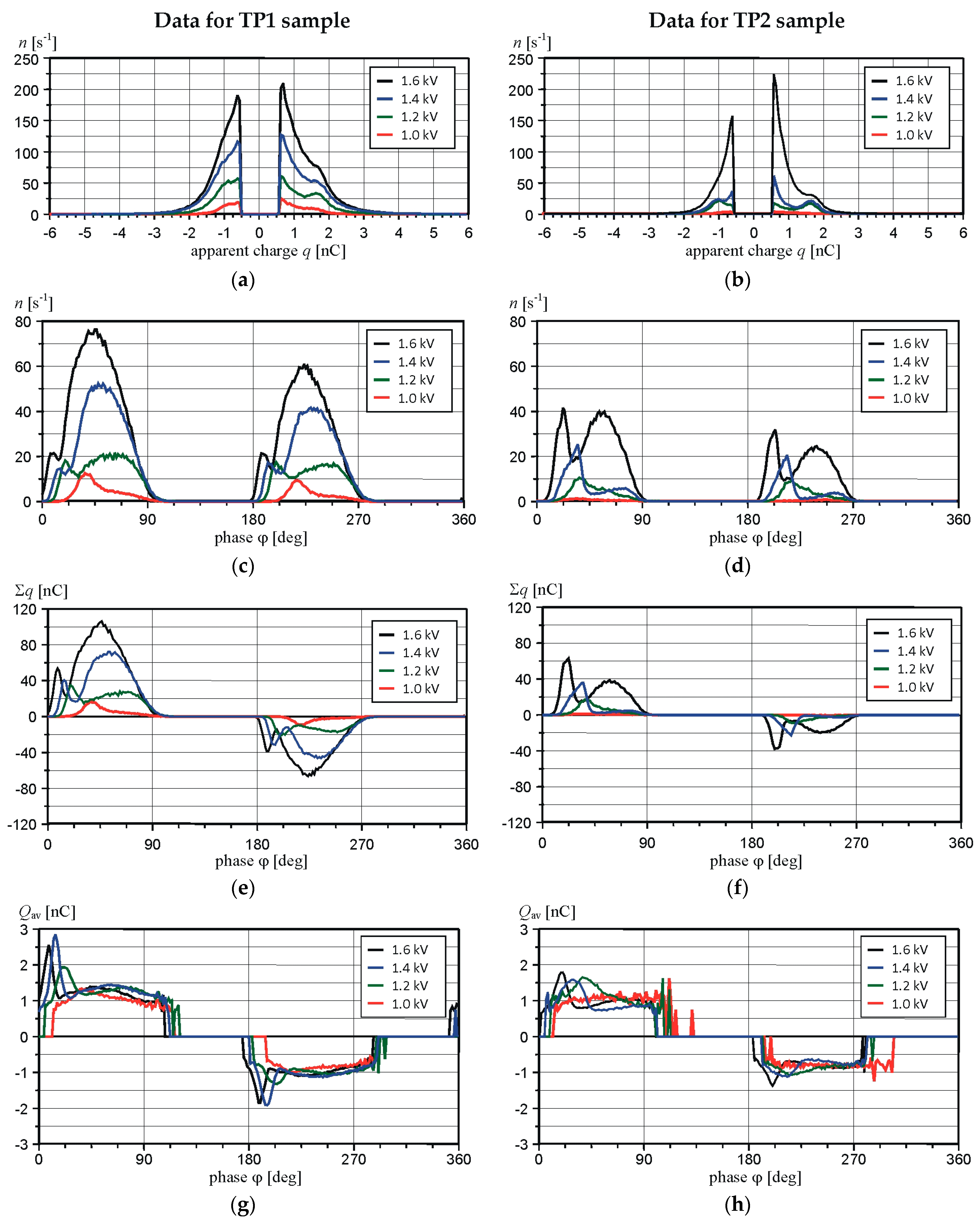
Figure 24.
Calculated PD parameters: (a) pulse number per second N; (b) the average apparent charge Qav vs. test voltage (both polarities of PD pulses registered for samples TP1 and TP2).
Figure 24.
Calculated PD parameters: (a) pulse number per second N; (b) the average apparent charge Qav vs. test voltage (both polarities of PD pulses registered for samples TP1 and TP2).

Table 1.
Breakdown voltage UBD for samples TP0.3 and TP0.8 for a different number of twists ts.
| Sample Type | Breakdown Voltage UBD [kV] | ||||
|---|---|---|---|---|---|
| ts = 1 | ts = 3 | ts = 5 | ts = 10 | ts = 15 | |
| TP0.3 | 11 | 10.2 | 10.0 | 9 | 8 |
| TP0.8 | 21.0 | 20.0 | 19.6 | 17.5 | 17.2 |
© 2019 by the authors. Licensee MDPI, Basel, Switzerland. This article is an open access article distributed under the terms and conditions of the Creative Commons Attribution (CC BY) license (http://creativecommons.org/licenses/by/4.0/).
Share and Cite
MDPI and ACS Style
Florkowski, M.; Florkowska, B.; Zydron, P. Partial Discharges in Insulating Systems of Low Voltage Electric Motors Fed by Power Electronics—Twisted-Pair Samples Evaluation. Energies 2019, 12, 768. https://doi.org/10.3390/en12050768
AMA Style
Florkowski M, Florkowska B, Zydron P. Partial Discharges in Insulating Systems of Low Voltage Electric Motors Fed by Power Electronics—Twisted-Pair Samples Evaluation. Energies. 2019; 12(5):768. https://doi.org/10.3390/en12050768
Chicago/Turabian StyleFlorkowski, Marek, Barbara Florkowska, and Pawel Zydron. 2019. "Partial Discharges in Insulating Systems of Low Voltage Electric Motors Fed by Power Electronics—Twisted-Pair Samples Evaluation" Energies 12, no. 5: 768. https://doi.org/10.3390/en12050768
Note that from the first issue of 2016, this journal uses article numbers instead of page numbers. See further details here.