Equivalent Two Switches and Single Switch Buck/Buck-Boost Circuits for Solar Energy Harvesting Systems


1
ECAM Strasbourg Europe-ICube Laboratory (UMR7357), F-67400 Illkirch-Graffenstaden, France
2
Institut Jean Lamour (UMR7198), Université de Lorraine, 54011 Nancy, France
*
Authors to whom correspondence should be addressed.
Energies 2020, 13(3), 583; https://doi.org/10.3390/en13030583
Submission received: 17 December 2019
/
Revised: 9 January 2020
/
Accepted: 21 January 2020
/
Published: 27 January 2020
(This article belongs to the Special Issue Solar Energy Harvesting, Storage and Application)
Abstract
:In this paper, a comparative analysis has been presented of two equivalent circuits of non-isolated buck/buck-boost converters under synchronous control, used in a stand-alone Photovoltaic-battery-load system. The first circuit consists of two cascaded buck and buck-boost classical converters with two controllable switches. The buck converter is used to extract the maximum power of the Photovoltaic source, and the buck-boost converter is applied for the output voltage level control. The second circuit consists of a proposed converter with a single controllable switch. In both cases, the switching frequency is used to track the maximum power point and the duty ratio controls the output voltage level. Selected simulation results and experimental tests confirm that the two conversion circuits have identical behavior under synchronous control. This study shows that the single switch converter has a lower size and cost, but it is limited in the possible control strategy.
1. Introduction
Due to the increasing environmental concerns, many research studies have targeted the use of Renewable Energy Sources (RES) as an alternative to fossil fuels. Thus, solar Photovoltaic (PV) energy harvesting systems have a remarkable growth and a significant penetration in many fields of application. In this paper, among the various applications of PV energy harvesting systems, we study a stand-alone Photovoltaic-battery-load system, classically based on the non-isolated two-stage DC-DC electronic conversion [1,2,3,4,5,6]. The rechargeable battery eliminates DC-link capacitor voltage stress; moreover, it allows energy storage for when the produced PV solar energy is larger than what is required by the load. One of the most suitable non-isolated two-stage DC-DC electronic conversions for stand-alone PV systems is based on a well-known buck converter that is cascaded with a buck-boost one, as presented in Figure 1 [2]. Two switches are classically used for the cascaded DC-DC conversion, where each switch contributes individually and significantly to power dissipation. Effectively, in the repeated energy management process, the energy is transmitted from the PV source to the load by flowing from the first stage (buck converter) to the second one (buck-boost converter). In a general manner, a high number of switches indicate a high system cost and physical size. Particularly, a reduced number of switches in a circuit can decrease switch drivers and simplify control circuits as well. Thus, the resulting system size is also reduced. Further, the driving circuit design is facilitated.
Therefore, one possible way to decrease the cost and size of the above-mentioned stand-alone PV energy harvesting systems is to apply a unified approach to form an equivalent converter with a single switch instead of using two switches (one for each cascaded conversion stage). In this spirit, an approach based on Synchronous Switches (SS) was first proposed by T. Wu and T. Yu; this approach was mainly dedicated to aerospace applications for weight, size and cost purposes [3]. They have introduced four SS corresponding to the four common node types of two active switches. Nevertheless, it is noticeable that the design approach presented in [3] is applicable only when the two switches of the cascaded DC-DC conversions are turned ON/OFF synchronously. That is why in the rest of the paper, the considered two switches and single switch are so called “Equivalent Synchronous Switches (ESS).”
In this paper, we propose to “modify,” step by step, the traditional MOSFET-based two-stage buck/buck-boost circuit, depicted in Figure 1, to make it finally equivalent to an electrical circuit based on a single switch. Two constraints must be satisfied to replace the two switches by a SS: first, the two switches must share a common node and second, they must be turned ON and OFF synchronously. Thus, the modified conversion circuit with a single switch can have the same behavior as when the two switches are operating individually [3]. Here, as detailed in the following section, by moving the two switches toward each other, the usual circuit in Figure 1 can be “modified” step by step to make a two-switch common node of a drain-source connection type, called the “DS: I-II type”, appear according to [3]. Then, by replacing the two switches by the corresponding ESS (here called the “Inverted IISS:I-IISS”, [3]), the resulting and equivalent circuit based on a single switch is obtained.
Let us now consider the control of the solar PV energy harvesting system. Firstly, it is mandatory to perform Maximum Power Point Tracking (MPPT) in order to maximize the extracted energy, irrespective of the irradiance conditions [7]. Secondly, the output voltage of the PV system must be also regulated for load feeding considerations. The conventional two-stage DC-DC converter presented in Figure 1 can perform MPPT and output voltage regulation simultaneously [8]. When the two switches of the buck and buck-boost converters are synchronously controlled, the duty cycle and the switching frequency are controlled independently to perform these two tasks simultaneously [9]. In the modified converter based on the ESS, the control parameters are the same and are applied to the single switch. Here, among the usual MPPT techniques, the Perturb and Observe (P&O) algorithm appears as the best compromise, performing good tracking factors, simple implementation and satisfactory accuracy [10].
In the next section, the design of the single switch converter from the conventional two-stage circuit presented in Figure 1 is developed. The major design steps are detailed in order to combine the buck and buck-boost converters to form the ESS circuit under synchronous control. In addition, the operation principle of the ESS circuit is discussed, mainly based on the energy exchange modes. The control, including simultaneous MPPT and output voltage regulation, is studied in Section 3. The modeling of the resulting Photovoltaic-battery-load system is presented in Section 4, and is based on the ESS conversion circuit. The PV panel and battery models are also briefly discussed. Then, some selected simulation results are provided and discussed to validate the equivalence between the two circuits, which are based on two switches or on a single switch. Experimental results are presented in Section 5. Finally, in Section 6, some conclusions are drawn.
2. Equivalent Two-Switches and Single Switch Buck/Buck-Boost Circuits
2.1. Topology Derivation
In the literature, a two-stage DC-DC converter, as presented in Figure 1, is commonly used to simultaneously perform the MPPT and the output voltage regulation of the solar PV system. In this case, each DC-DC stage is independently controlled, whatever the applied control. The control signals driving the gate voltage of each transistor for each DC-DC stage can be generated asynchronously or synchronously. Besides, the frequency of these two control signals is usually the same. As mentioned before, the synchronous control case is considered in this study to allow for the design of the single switch conversion circuit, which is based on [3].
When the converter presented in Figure 1 is driven synchronously, one unique control signal is used to drive the two transistors. Thus, the control signals (also called switching patterns) of each DC-DC stage are the same and, thus, have the same frequency and the same duty ratio. The synchronous operating mode cannot be performed if the two DC-DC stages operate in the continuous operation mode: either the first converter is in the Discontinuous Conduction Mode (DCM) whereas the second one is in the Continuous Conduction Mode (CCM), or vice versa. In this study, to avoid any DCM for the load, the duty ratio of the switching pattern is used to regulate the output voltage delivered to the load, whereas its frequency is the MPPT control parameter.
The circuit presented in Figure 1 can be restructured as presented in Figure 2. To have a common node, both transistors are moved toward each other, thus having the drain of the switching transistor connected to the source of the switching transistor . According to [3], two synchronous switches that have a common drain-source node and are in the configuration, as presented at the left of Figure 3, can be replaced with an ESS, as presented at the right of the same figure. In the topology presented in Figure 2, the diodes and in Figure 3 cannot be identified. However, if these two diodes are added to the initial topology (Figure 2), as presented in Figure 4, its operation will not be affected because of the two added diodes and are never conducting: they are reverse biased either by the PV cell and the battery or by the negative load voltage.
Thus, the two-stage DC-DC circuit (Figure 1) can be replaced with the single switch circuit (Figure 5, bottom), under synchronous control. This DC-DC circuit can be now used throughout this work in all further sections.
It is clear that the proposed single switch design saves a MOSFET and its associated gate driver, but it adds two diodes in the circuit. However, only the extra MOSFET gate driver used in the two-stage converter costs much more than the two diodes added in the single switch circuit. Further, the additional costs for the control circuit design are not considered here. Thus, from an economical point of view, the overall cost of the two-stage buck/buck-boost circuit is slightly higher than the one of the single switch circuit. At low power, the amount of the savings that are realized when using the single switch converter can seem low. Nevertheless, such cost consideration is very important when consumer applications using solar energy harvesting are targeted.
2.2. Principle and Operating Modes of the Single Switch Circuit
The operation modes of the circuit derived in the previous section are presented in Figure 6. The battery is assumed to be fully charged to its operating voltage (12 V in this work). Four operation modes can be distinguished, and each one is characterized by different energy exchanges between the PV cell, the battery and the connected load. These energy exchanges are presented in red in Figure 6. The two previously mentioned conduction modes (DCM and CCM) can be seen in Figure 6 by observing the shape of the inductor currents and .
In the first operating mode, the energy flows directly from the PV cell to the inductor through the inductor , and partially from the battery and the capacitor to the inductor . In this operating mode, the load is disconnected from the PV cell and the battery (the diode is not conducting), and is only supplied by the energy stored in the capacitor ; the two diodes and are not conducting, whereas the diode and the switching transistor S’1 are conducting. This operating mode starts with the ON state of the switching transistor and ends when the inductor current outreaches the value. The slopes of the inductor currents and are, respectively:
The second operating mode is also during the ON state of the switching transistor while . In this mode, the energy extracted from the PV cell charges up not only the inductor , but also the battery and the capacitor . Unlike in the first operating mode, the diode is conducting, whereas the diode is reverse biased. Thus, the sum of the currents supplied by the battery and the capacitor flows through the diode . As in the first operating mode, the load is disconnected from the PV cell and the battery (the diode is not conducting) and is only supplied with the energy stored in the capacitor . At the end of this operating mode, the currents and reach their maximal values and:
where is the average value of the inductor current .
The third and fourth operating modes occur while the switching transistor is OFF. In these operating modes, the connected load is supplied by the energy previously stored in the inductor . This ’s energy is also used to recharge the capacitor , whose main function is to feed the connected load during the ON state of . In the third operating mode, besides the switching transistor, the diodes and are not conducting, whereas the diode is conducting. The diode conduction allows it to completely discharge the inductor through the battery and the capacitor . The discharge slopes of the inductors and are given with the following expressions:
In the fourth operating mode, all diodes except the diode are reverse biased. The direct biased diode ensures that the energy previously stored in the inductor is transferred to both the capacitor and the load. The fourth operating mode ends with the ON state of the switching transistor, which puts the topology in the first operating mode.
In the single switch circuit, when the switch S is on, it provides a current path for both the battery and the solar source. Thus, the use of a single switch reduces repeated power processing that is classically done when energy is transmitted from the first stage to the second one. Consequently, power losses are reduced from this point of view. Nevertheless, the MOSFET S must be chosen based on a main criterion; it is low turn-on resistance that will reduce the conduction losses in the single stage circuit. The challenges and progress in microelectronic technology aim to contribute to the reduction of this resistance.
Based on the previous operating modes of the circuit, the relationship between the output voltage and the battery’s voltage as well as the relationship between the PV panel and converter parameters can be established. As it has been stated, to ensure the correct functioning of this converter, the inductors and must be in different conduction modes: the inductor in the DCM while the inductor in the CCM. Under these conditions, and taking into account that the battery’s voltage can be considered constant over time, the output voltage can be expressed as follows:
where is the duty cycle of the switching pattern driving the switching transistor . Consequently, it can be seen that the output voltage is controlled only by adjusting the duty cycle of the single control signal, which is applied to .
On the other hand, the current flowing through the PV panel is the same as the one through when the switch is ON. The average value of the PV current () can be written as a function of duty cycle in Equation (8):
and while operates in DCM, the value can be calculated as follows:
By replacing Equation (9) in Equation (8), the relationship between and the control variables becomes:
As mentioned before, the value of the duty cycle is determined by the reference value of the output voltage . Accordingly, by measuring the PV panel current and its voltage , and by knowing the value of the duty cycle , the maximum power point can be tracked by controlling the frequency of the control signal applied to . It should also be noted that in the steady conditions under uniform irradiance where and are constant (a unique MPP), the new reference value of the output voltage involves the changes of both the duty cycle and, consequently, the frequency to maintain the MPPT.
3. Control of the Equivalent Single Switch Buck/Buck-Boost Circuit
In the proposed solar PV energy harvesting system, two parameters must be controlled: the PV power generation and the output voltage. A PV array under uniform irradiance has a unique Maximum Power Point (MPP), where the array produces maximum output power. This MPP (as well as I-V characteristic of a PV array) changes with the variation of the irradiance level and the panels’ temperature [11]. Therefore, to maximize the power produced by the solar PV energy harvesting system, the MPP should be tracked continuously by a MPPT algorithm. In recent years, several MPPT techniques were developed. In the scientific literature, some techniques that do not depend on the characteristic parameters of the PV module are proposed, such as incremental conductance and Perturb and Observe (P&O) [12,13]. Moreover, they are widely used in commercial products due to their ease of implementation [11,14].
MPPT is not the goal of this paper. Thus, a classical P&O technique based on the control of the frequency of the switching pattern is applied to the single switch circuit (Figure 5, bottom). In addition, two classic Proportional Integral (PI) controllers are used in order to control the output voltage of the circuit by the duty cycle of the applied switching pattern. As illustrated in Figure 7, the duty cycle () regulates the output voltage, and the MPPT is done by the switching frequency . The output voltage regulation (V0 control in Figure 7) of the solar PV energy harvesting system is detailed later in this paper.
As mentioned previously, the inductor must work in CCM while the inductor must work in DCM. In this condition and in steady-state operation mode, the relationship between and is expressed by Equation (7). By considering a constant value () for the voltage across the battery, the output voltage can be controlled by the duty cycle ().
Figure 7 (bottom) shows a block diagram of the output voltage controlled by two PI controllers. As this figure shows, two traditional controllers are used: the first PI is applied to control and the second PI is for . To design the PI controllers, the transfer functions for the single switch circuit have to be defined. Based on a small signal model of the circuit, two essential transfer functions are determined as follows:
The parameters of the PI controllers can be defined by using the Bode diagram method.
4. Modeling and Simulation of the Solar PV Energy Harvesting System
4.1. Photovoltaic Cell
In this paper, a model with a moderate complexity of a PV cell is used. This model consists of a current source in parallel with a diode and a series resistance. The current of the source () is directly proportional to the light falling on the cell. Increasing sophistication, accuracy and complexity can be introduced to the model by adding some parameters such as the temperature dependence of the diode saturation current [15,16,17]. The current of the PV cell is the difference between the photo current and the normal diode current:
where is the idealizing factor, is the Boltzmann’s gas constant, the absolute temperature of the cell, the electron charge and is the dark saturation current, which depends on the temperature.
4.2. Battery
A commonly used battery model proposed in [18,19,20] is used in this study. Equation (14) expresses the relationship of the battery voltage [18,20]:
where is the terminal voltage, is the open-circuit voltage, is the charge/discharge current, is the internal resistance and a parallel RC circuit illustrates the charge transfer and the diffusion between the electrodes and the electrolyte [7,20].
It is noticeable that the capacitance is sufficiently large such that is taken as a constant value during the modeling stage.
4.3. System Parameters
The parameters of the solar PV energy harvesting system, based on the buck/buck-boost circuit, are given in Table 1. To determine the parameters of the PI controller, first, the transfer functions ( and ) are defined by using the element’s value presented in Table 1. Then by using Bode diagram, the suitable value of controller parameters are chosen for each controller separately. Two applied controllers are presented in the following:
4.4. Selected Simulation Results
Under synchronous control, in order to validate the equivalence between the two conversion circuits that were either based on the two switches S1 and S2, or based on the single switch S’1, the solar energy harvesting system (Figure 5, top and bottom) was simulated in the two cases for the same parameters provided in Table 1. Simulations were performed in the MATLAB/Simulink environment. A variation of the irradiance G was applied to the PV array, with a time varying from 400 W/m2 to 1000 W/m2.
In the case of the circuit based on the two switches S1 and S2 (Figure 5, top), a global vision of the simulation results is provided in Figure 8. In the time interval [], the irradiance level increases from 400 W/m2 to 1000 W/m2 and the panel temperature is set to 25 °C. In these conditions, according to the PV characteristic curve, the maximal extracted power increases from W to W. To reach the instantaneous maximum power point, the switching frequency decreases continuously from 92 kHz to 52.5 kHz (according to Equation (10)) as long as the duty cycle D remains constant and fixed to 0.525. This value of D corresponds to an output voltage level equal to 13 V. At each instant, the PV produces its maximum power, and it is noticeable that the output voltage remains regulated and constant.
At the time t = 0.5 s, the output voltage reference is stepped-up to ; consequently, the value of D is stepped-up from 0.525 to 0.575, and thus, the frequency parameter is modified accordingly and increases, as according to Equation (10). Indeed, as previously mentioned, a new reference value of the output voltage involves the changes of both the duty cycle , and consequently the frequency to maintain the efficiency of the MPPT function.
Then, in the second part of the presented simulation results (Figure 8), the irradiance level decreases from 1000 W/m2 to 400 W/m2 and the panel temperature is always set to 25 °C. Moreover, at the time t =1.5 s, the output voltage reference is stepped-down to . During the decrease of the irradiance G, the switching frequency increases from 52.5 kHz to 100 kHz (according to Equation (10)) as long as the duty cycle D remains constant and fixed to 0.575, which corresponds to an output voltage level equal to 16 V.
At the time t = 1.5 s, the output voltage reference is stepped-down to ; consequently, the D value is stepped-down from 0.575 to 0.560, and thus, the frequency parameter is modified accordingly and decreases, as according to Equation (10). One can notice that the output voltage () is always regulated by the PI controllers and stabilized around its reference value.
For the conversion circuit based on two switches S1 and S2, Figure 9 shows some zoomed results in steady-state and for a fixed point with an output voltage control reference equal to 16 V and an irradiance G equal to W/m2 This figure illustrates the currents and as well as the duty cycle D and the switching frequency f. From the presented results, it can be seen that the inductor has a positive average current value and does not cross the zero line, which indicates that the inductor is operating in the continuous conducting mode. On the other hand, the average current of is smaller than and is equal to zero over a part of a period, which means that the inductor is in discontinuous conducting mode. The obtained results are in accordance with the operating modes presented in Section 2.2. For the selected fixed point, the values of D and f are about 0.575 and 63 kHz, respectively.
Let us now consider the case of the circuit based on the single switch S’1 (Figure 5, bottom). A global vision of the simulation results is also provided in Figure 10 where the same parameters’ variations are applied (f and D), as in the previous case. One can notice that the obtained results are similar to the one obtained for the conversion circuit based on the two switches, S1 and S2, and they are presented in Figure 8.
Always in the case of the circuit based on the single switch S’1 (Figure 5, bottom), a detailed focus is made on the inductance and currents crossing, as well as the time variations of the frequency f and the duty cycle D. The selected simulation results are presented in Figure 11 for the same voltage reference equal to 16 V and irradiance G equal to W/m2 as the one applied in the previous case (see Figure 9). Once again, these results are in accordance with the operating modes presented in Section 2.2. For the same conditions, the values of f and D are quite different from the values presented in Figure 9 about 0.58 (instead of 0.575) and 67 kHz (instead of 63 kHz), respectively. One can explain this minor difference by the operating modes (and consequently the current paths) that are not the same for the two studied equivalent circuits.
5. Experimental Results
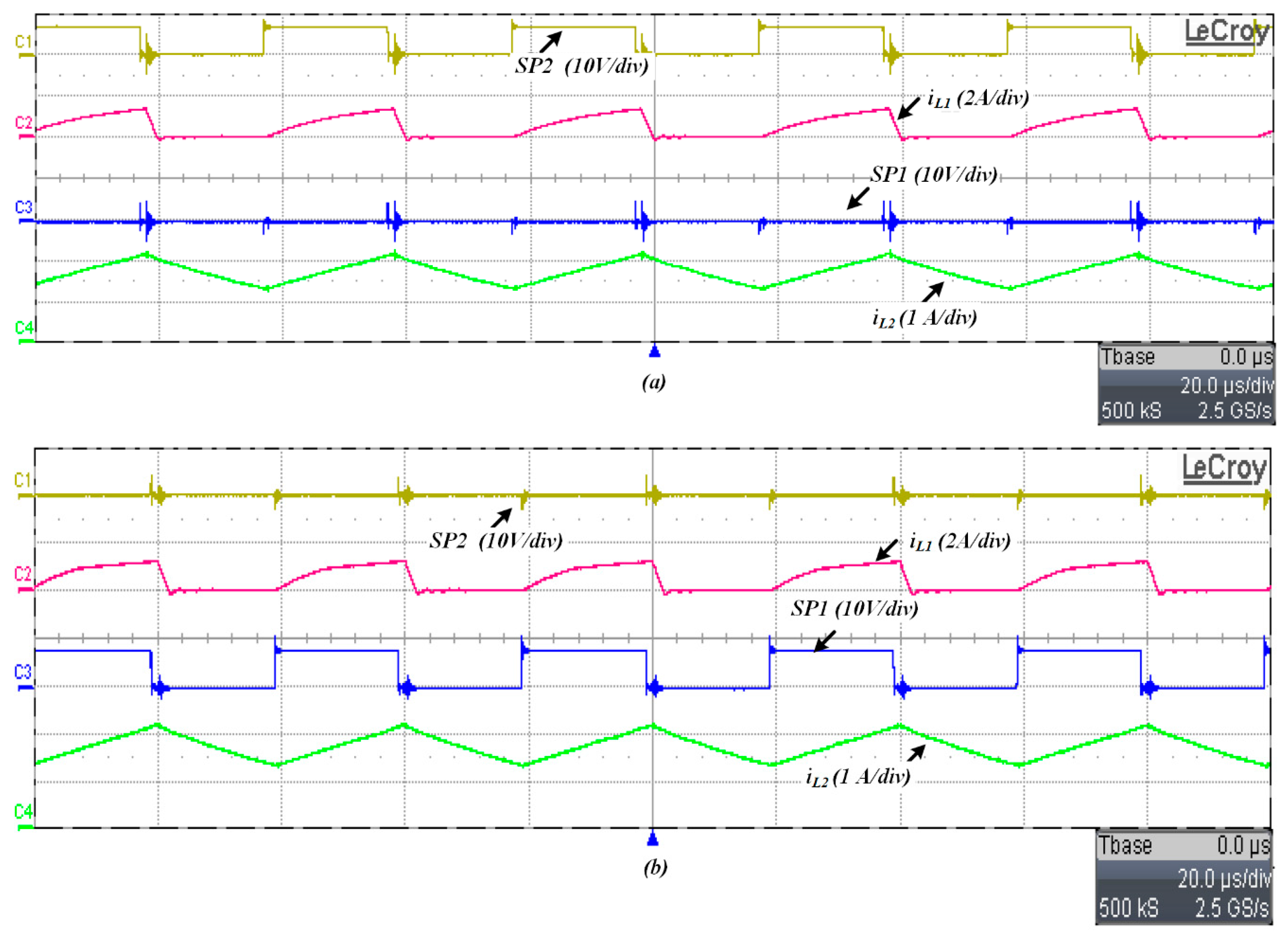
Figure 12 shows the realized experimental test bench based on the prototype circuit with the parameters provided in Table 1 for the buck/buck-boost circuit, battery and load. This circuit comprises the two equivalent circuits previously presented in Figure 5 (top and bottom). The two switches S1 and S2 of the buck/buck-boost circuit (Figure 5, Top) are synchronously controlled by the Switching Pattern SP2, while the single switch S of the buck/buck-boost circuit (Figure 5, Bottom) is controlled by the switching pattern SP1. The switches we used are IRFP4110 MOSFET devices from International Rectifier, and the diodes are MBR10100 Diodes from ON Semiconductor.
This paper focuses on the equivalence between the two circuits presented in Figure 5. Thus, for the experimental test, we have chosen a fixed operating point where the PV panel is replaced by a DC source. This point corresponds to a 20 W power where and . The control depicted in Figure 7 is realized by a Dspace MicroLabBox.
The experimental results obtained for the circuit with two switches (circuit Figure 5, Top) are summarized in Figure 13a. In this case, a single switching pattern SP2 under synchronous control is applied to the two MOSFETs S1 and S2 (25 kHz frequency and 50% duty cycle). The switching pattern applied to S is fixed to ‘0’; thus, the MOSFET S is always in the OFF state. The shapes of the currents validate the conduction modes for the inductances and , in DCM and CCM, respectively.
The experimental results obtained for the circuit with one single switch (Figure 5, bottom) are summarized in Figure 13b. In this case, the switching pattern SP2 (applied to S1 and S2) is fixed to ‘0’; thus, these two MOSFETs are always in the OFF state. The same switching pattern as previously used (25 kHz frequency and 50% duty cycle) is now applied to S. The shapes of the inductor currents validate the conduction modes for the inductances and , in DCM and CCM, respectively.
Moreover, we can notice that the currents presented in Figure 13a,b have the same shape; thus, the two circuits can be considered as equivalent. One can notice that the waveforms of both inductance currents are not exactly the same. This can be explained by the current paths that are not exactly identical for the two equivalent circuits (as detailed in the “Operating Modes” subsection). Some paths generate some additional voltage drops that modify the slope and, consequently, the shapes of the inductance currents.
6. Conclusions
In this paper, to decrease the overall size, weight and complexity of stand-alone solar Photovoltaic-battery-load energy harvesting systems, we have proposed a unified approach that consists of forming an equivalent two-stage DC-DC conversion circuit with a reduced switch number. This resulting circuit is based on a single switch instead of using two switches. Indeed, one switch is usually used for each one of the two cascaded DC-DC conversion stages. This reduction of the number of switches lays on the ESS, studied by T. Wu and T. Yu in [3]. Thus, the two “equivalent” circuits presented in Figure 5 (top and bottom) are identical only if a synchronous control of the converter is applied. This suggests that the two parameters f and D of the single switching pattern, applied for both DC-DC conversion circuits, are used for MPPT tracking and output voltage control, respectively.
In the previous sections, the design, as well as the operating modes of the single switch conversion circuit, are detailed. Mainly, the different conduction modes (DCM and CCM) of the two inductances are discussed. The choice of the CCM for the load side of the converter is justified. In steady-state condition, one switching period of the single switch converter goes through four operation modes, during which the inductors and must work in DCM and CCM, respectively. The control of the converter was also studied.
The Photovoltaic-battery-load power system was modeled with MATLAB/Simulink environment and the obtained simulation results confirm the equivalence between the two conversion circuits in terms of control effectiveness and system performances. In addition, experimental results also confirm the equivalence between the two circuits. Thus, it is concluded that the studied stand-alone PV system relying on a single switch circuit can efficiently realize the same functionalities as the one using the usual two-stage conversion based on two switches, with lower size and cost. Although, the degrees of control freedom for the single switch converter are reduced and more sophisticated, control modes can be used for the circuit presented in Figure 1. The single switch converter must be synchronously controlled, as previously mentioned, to have the same behavior as the two-stage circuit.
Author Contributions
Investigation, E.J., P.P. and S.J.; Resources, E.J., P.P. and S.J.; Writing—review and editing, E.J., P.P. and S.J. All authors have read and agreed to the published version of the manuscript.
Funding
This research received no external funding.
Conflicts of Interest
The authors declare no conflict of interest.
References
- Caracas, J.V.M.; de Carvalho Farias, G.; Teixeira, L.F.M.; de Souza Ribeiro, L.A. Implementation of a high-efficiency, high-lifetime, and low-cost converter for an autonomous photovoltaic water pumping system. IEEE Trans. Ind. Appl. 2014, 50, 631–641. [Google Scholar] [CrossRef]
- Vighetti, S.; Ferrieux, J.; Lembeye, Y. Optimization and design of a cascaded dc/dc converter devoted to grid-connected photovoltaic systems. IEEE Trans. Power Electron. 2012, 27, 2018–2027. [Google Scholar] [CrossRef]
- Wu, T.F.; Yu, T.H. Unified approach to developing single-stage power converters. IEEE Trans. Aerosp. Electron. Syst. 1998, 34, 211–223. [Google Scholar]
- Chewale, M.A.; Wanjari, R.A.; Savakhande, V.B.; Sonawane, P.R. A Review on Isolated and Non-isolated DC-DC Converter for PV Application. In Proceedings of the 2018 International Conference on Control, Power, Communication and Computing Technologies (ICCPCCT), Kannur, India, 23–24 March 2018; pp. 399–404. [Google Scholar]
- Elmakawi, A.M.; Bayındır, K.Ç. Novel Single Switch High Gain Non-isolated DC-DC Converter for Building Integrated Photovoltaic Systems. In Proceedings of the 2019 1st Global Power, Energy and Communication Conference (GPECOM), Nevsehir, Turkey, 12–15 June 2019; pp. 265–269. [Google Scholar]
- Singh, G.; Srivastava, S.; Lalwani, R.; Tewari, N.; Prabhakar, M. High Gain DC-DC Converter Based on Hybrid Switched-Inductor Topology for PV Application. In Proceedings of the 2019 IEEE International Conference on System, Computation, Automation and Networking (ICSCAN), Pondicherry, India, 29–30 March 2019; pp. 1–6. [Google Scholar]
- Liu, G.; Zhu, J.; Tao, H.; Wang, W.; Blaabjerg, F. A MPPT Algorithm based on PSO for PV Array Under Partially Shaded Condition. In Proceedings of the 22nd International Conference on Electrical Machines and Systems (ICEMS), Harbin, China, 11–14 August 2019. [Google Scholar]
- Taghvaee, M.; Radzi, M.; Moosavain, S.; Hizam, H.; Marhaban, M.H. A current and future study on non-isolated dc-dc converters for photovoltaic applications. Renew. Sustain. Energy Rev. 2013, 17, 216–227. [Google Scholar] [CrossRef]
- An, L.; Lu, D.C. Design of a single-switch dc/dc converter for a pv-battery-powered pump system with pwm control. IEEE Trans. Ind. Electron. 2015, 62, 910–921. [Google Scholar] [CrossRef]
- Kim, J.; Cha, H. A Novel Variable Step sized MPPT Control based on P&O Method for Photovoltaic System. In Proceedings of the 22nd International Conference on Electrical Machines and Systems (ICEMS), Harbin, China, 11–14 August 2019; pp. 1–5. [Google Scholar]
- Femia, N.; Petrone, G.; Spagnuolo, G.; Vitelli, M. Optimization of perturb and observe maximum power point tracking method. IEEE Trans. Power Electron. 2005, 20, 963–973. [Google Scholar] [CrossRef]
- Lee, H.S.; Yun, J.J. Advanced MPPT Algorithm for Distributed Photovoltaic Systems. Energies 2019, 12, 3576. [Google Scholar] [CrossRef] [Green Version]
- Lopez-Lapena, O.; Penella, M.T.; Gasulla, M. A closed-loop maximum power point tracker for subwatt photovoltaic panels. IEEE Trans. Ind. Electron. 2011, 59, 1588–1596. [Google Scholar] [CrossRef]
- Bianconi, E.; Calvente, J.; Giral, R.; Mamarelis, E.; Petrone, G.; Ramos-Paja, C.; Spagnuolo, G.; Vitelli, M. A fast current-based mppt technique employing sliding mode control. IEEE Trans. Ind. Electron. 2013, 60, 1168–1178. [Google Scholar] [CrossRef]
- Jena, D.; Ramana, V. Simple and accurate method of modeling photovoltaic module: A different approach. In Proceedings of the 2013 International Conference on Green Computing, Communication and Conservation of Energy (ICGCE), Tamil Nadu, India, 12–14 December 2013; pp. 465–469. [Google Scholar]
- Suskis, P.; Galkin, I. Enhanced photovoltaic panel model for Matlab/simulink environment considering solar cell junction capacitance. In Proceedings of the IECON 2013—39th Annual Conference of the IEEE Industrial Electronics Society, Vienna, Austria, 10–13 November 2013; pp. 1613–1618. [Google Scholar]
- Pindado, S.; Cubas, J.; Roibás-Millán, E.; Bugallo-Siegel, F.; Sorribes-Palmer, F. Assessment of Explicit Models for Different Photovoltaic Technologies. Energies 2018, 11, 1353. [Google Scholar] [CrossRef] [Green Version]
- Tani, A.; Camara, M.; Dakyo, B. Energy management in the decentralized generation systems based on renewable energy ultracapacitors and battery to compensate the wind/load power fluctuations. IEEE Trans. Ind. Appl. 2015, 51, 1817–1827. [Google Scholar] [CrossRef]
- Chang, Y.C.; Chang, H.C.; Huang, C.Y. Design and Implementation of the Battery Energy Storage System in DC Micro-Grid Systems. Energies 2018, 11, 1566. [Google Scholar] [CrossRef] [Green Version]
- Jang, J.; Yoo, J.Y. Equivalent circuit evaluation method of lithium polymer battery using bode plot and numerical analysis. IEEE Trans. Energy Convers. 2011, 26, 290–298. [Google Scholar] [CrossRef]
Figure 1.
Classical two-stage buck/buck-boost DC-DC circuit based on two switches S1 and S2.

Figure 2.
Restructured circuit for Figure 1 with a common node of drain-source connection for the two switches.
Figure 2.
Restructured circuit for Figure 1 with a common node of drain-source connection for the two switches.
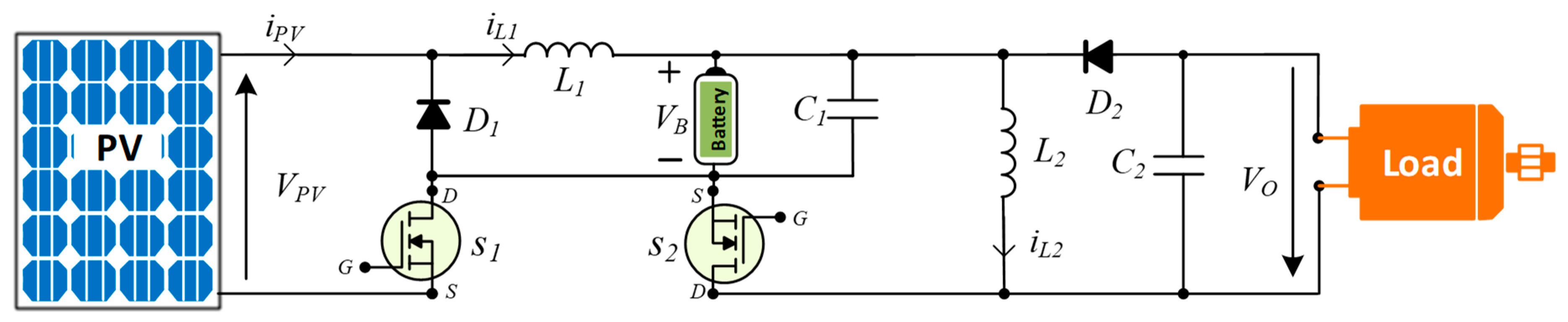
Figure 3.
Synchronous switches with a common drain-source node (type “DS: I-II type”, [3]) and its equivalent single switch topology (“Inverted IISS:I-IISS”, [3]).
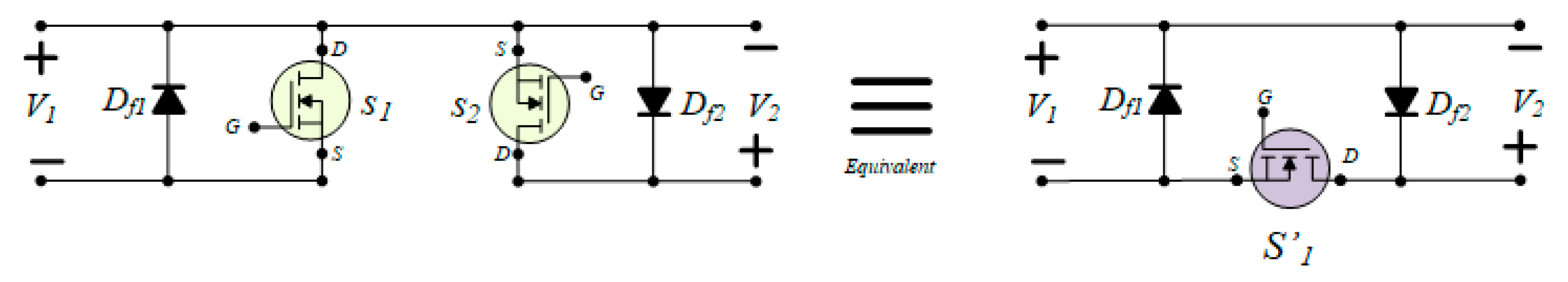
Figure 4.
The modified and electrically equivalent circuit from Figure 2. The added diodes (Df1 and Df2) do not modify its operation.
Figure 4.
The modified and electrically equivalent circuit from Figure 2. The added diodes (Df1 and Df2) do not modify its operation.

Figure 5.
Two-stage DC-DC converter (top) and its equivalent single switch circuit (bottom).

Figure 6.
Principle and operation modes of the equivalent single switch circuit.
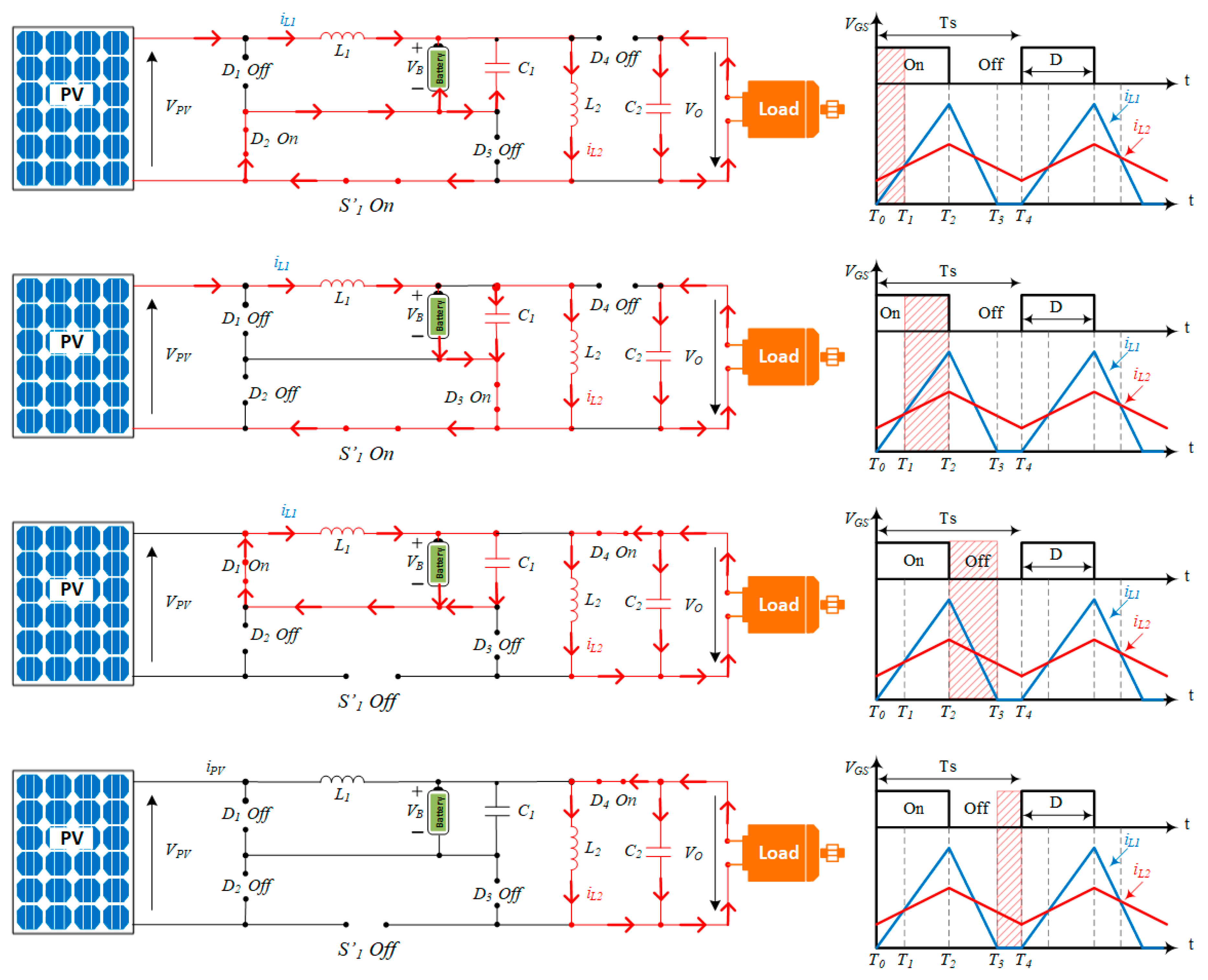
Figure 7.
Synoptic of the control applied to the equivalent single switch buck/buck-boost circuit.
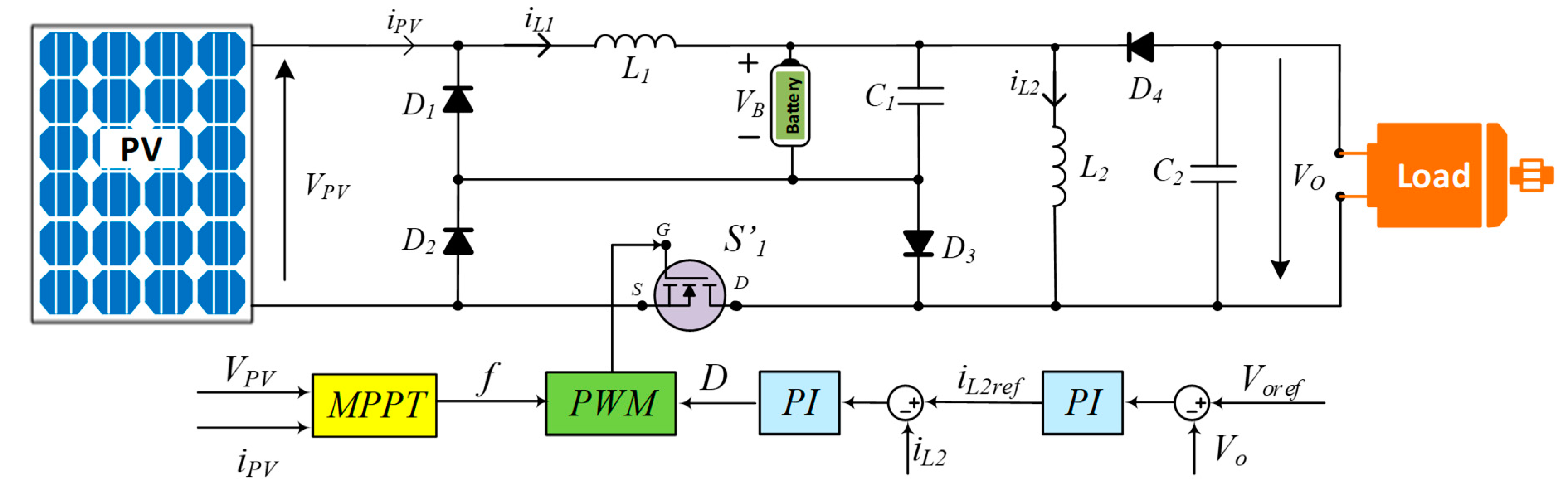
Figure 8.
Simulation results for the conversion circuit based on two switches S1 and S2 (Figure 5, top). From top to bottom: .
Figure 8.
Simulation results for the conversion circuit based on two switches S1 and S2 (Figure 5, top). From top to bottom: .

Figure 9.
Simulation results for the conversion circuit based on two switches S1 and S2 (Figure 5, top). From top to bottom: .
Figure 9.
Simulation results for the conversion circuit based on two switches S1 and S2 (Figure 5, top). From top to bottom: .
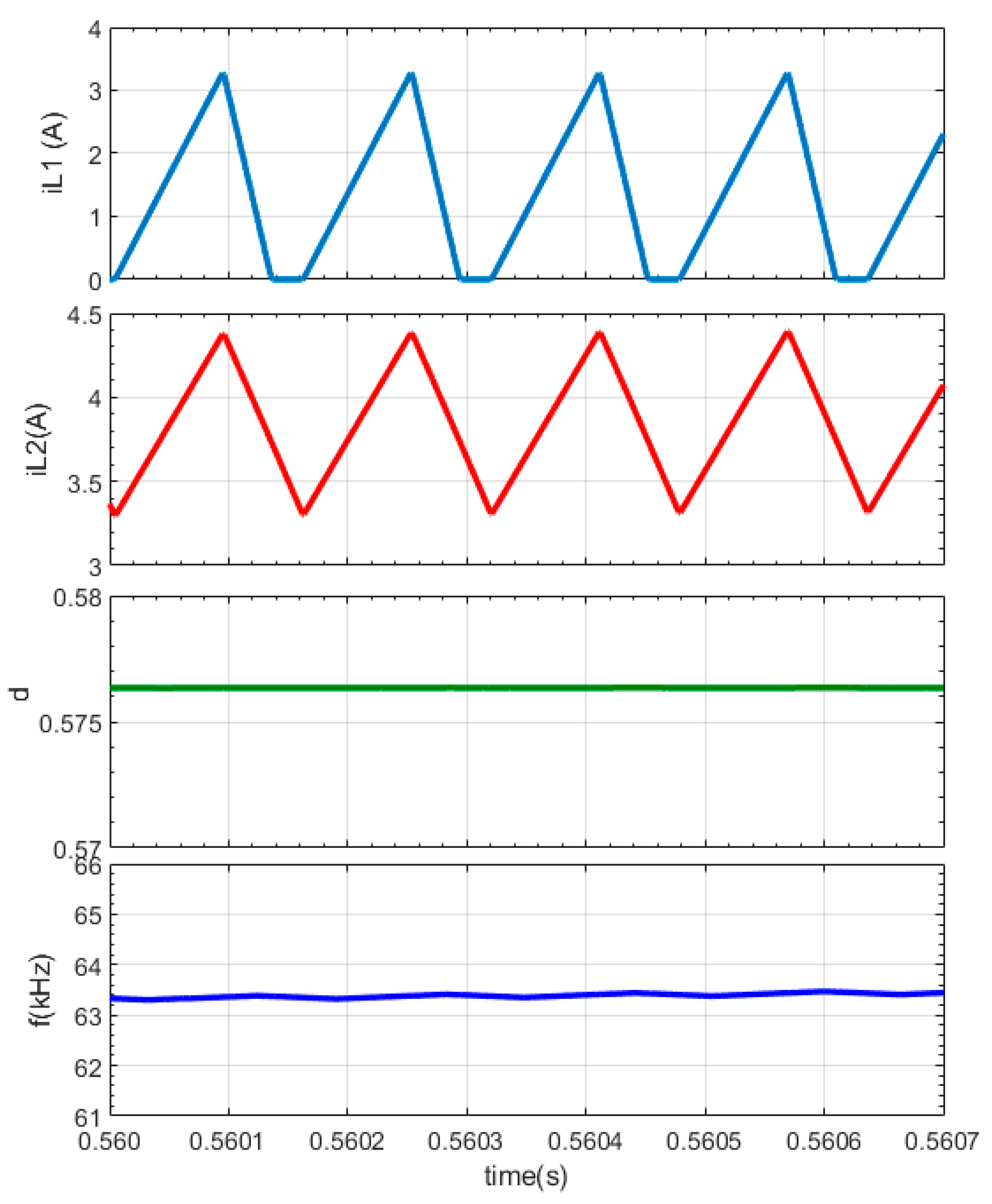
Figure 10.
Simulation results for the conversion circuit based on a single switch S’1 (Figure 5, bottom). From top to bottom: .
Figure 10.
Simulation results for the conversion circuit based on a single switch S’1 (Figure 5, bottom). From top to bottom: .
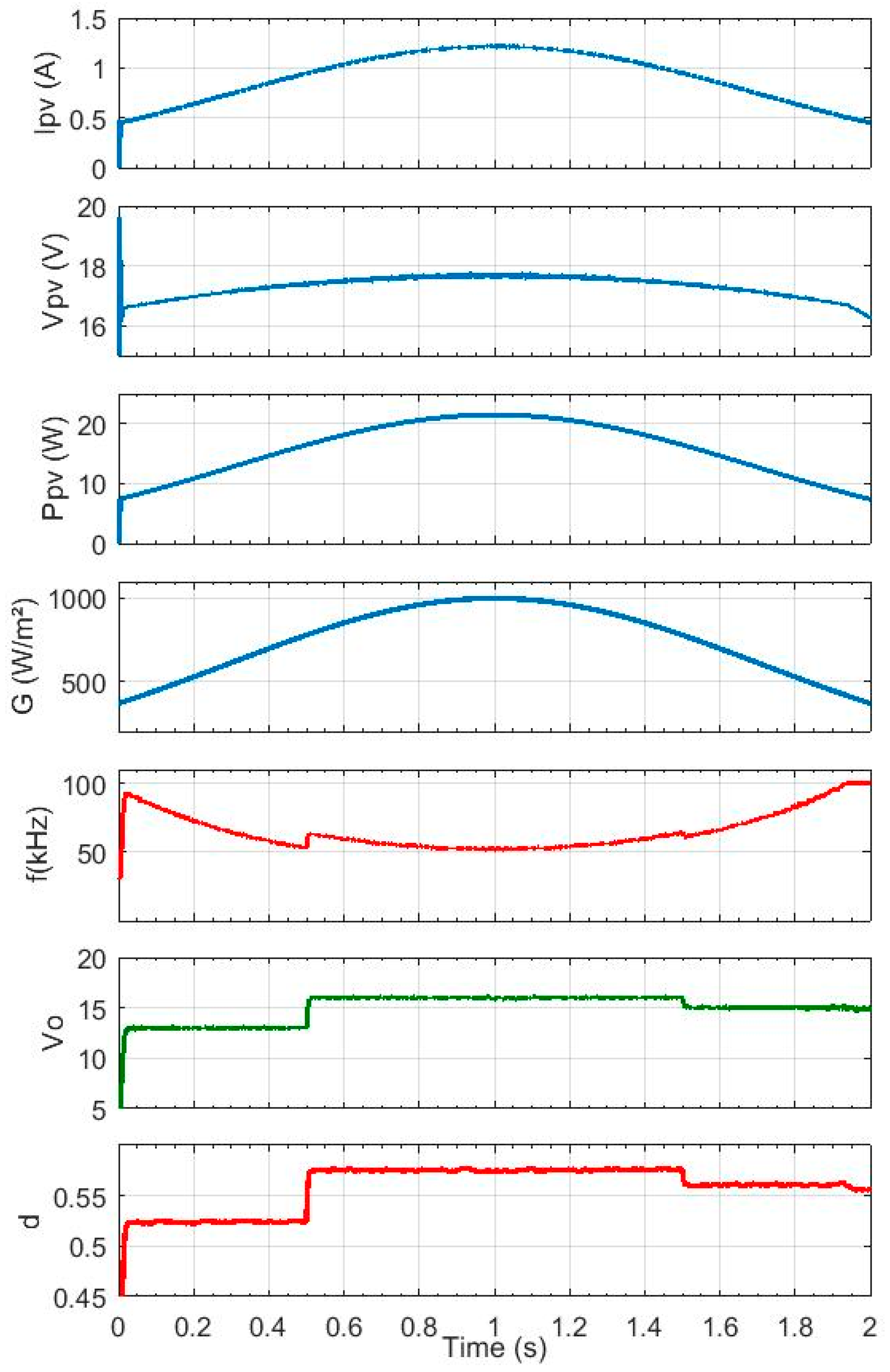
Figure 11.
Simulation results for the conversion circuit based on a single switch S’1 (Figure 5, bottom). From top to bottom: .
Figure 11.
Simulation results for the conversion circuit based on a single switch S’1 (Figure 5, bottom). From top to bottom: .
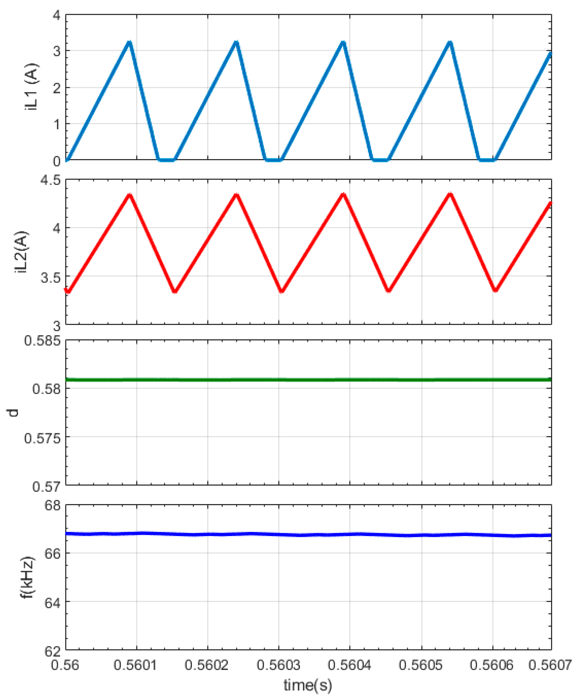
Figure 12.
Experimental setup for the two buck/buck-boost equivalent circuits.

Figure 13.
Experimental results for the buck/buck-boost circuit: (a) with two switches (Circuit Figure 5, Top) and (b) with a single switch (Circuit Figure 5, Bottom).

Table 1.
Parameters of the solar PV energy harvesting system.
| Elements | Value | |
|---|---|---|
| PV array | 0.65 A | |
| 21 V | ||
| 1.5 mΩ | ||
| 1011 Ω | ||
| 1.3 | ||
| 0.08 mA/K | ||
| Buck/buck-boost circuit, battery and load | ||
© 2020 by the authors. Licensee MDPI, Basel, Switzerland. This article is an open access article distributed under the terms and conditions of the Creative Commons Attribution (CC BY) license (http://creativecommons.org/licenses/by/4.0/).
Share and Cite
MDPI and ACS Style
Jamshidpour, E.; Jovanovic, S.; Poure, P. Equivalent Two Switches and Single Switch Buck/Buck-Boost Circuits for Solar Energy Harvesting Systems. Energies 2020, 13, 583. https://doi.org/10.3390/en13030583
AMA Style
Jamshidpour E, Jovanovic S, Poure P. Equivalent Two Switches and Single Switch Buck/Buck-Boost Circuits for Solar Energy Harvesting Systems. Energies. 2020; 13(3):583. https://doi.org/10.3390/en13030583
Chicago/Turabian StyleJamshidpour, Ehsan, Slavisa Jovanovic, and Philippe Poure. 2020. "Equivalent Two Switches and Single Switch Buck/Buck-Boost Circuits for Solar Energy Harvesting Systems" Energies 13, no. 3: 583. https://doi.org/10.3390/en13030583
Note that from the first issue of 2016, this journal uses article numbers instead of page numbers. See further details here.