Article

Efficiency Optimization for All-Silicon Carbide (SiC) PWM Rectifier Considering the Impact of Gate-Source Voltage Interference

1
School of Electrical Engineering, Institute of Power Electronics and Electric Traction, Beijing Jiaotong University, Beijing 100044, China
2
Power Supply Business Unit, Global Power Technology Co., Ltd., Beijing 100192, China
*
Author to whom correspondence should be addressed.
Energies 2020, 13(6), 1421; https://doi.org/10.3390/en13061421
Submission received: 18 February 2020 / Revised: 14 March 2020 / Accepted: 16 March 2020 / Published: 18 March 2020

Abstract

:
Compared with conventional silicon (Si)-based Pulse Width Modulation (PWM) rectifiers, PWM rectifiers based on silicon carbide (SiC) Metal-Oxide-Semiconductor Field-Effect Transistors (MOSFETs) have significant technical advantages and broad application prospects in terms of efficiency and power density, inherited from the high-speed switching feature. However, high-speed switching also induces gate-source voltage interference, which impacts the overall character of the conversion system. This paper considered the impact of gate-source voltage interference on loss, revealing an efficiency optimization for all-SiC PWM rectifiers. Firstly, this paper theoretically investigated the mechanism of improving the conversion system efficiency by using the 4-pin Kelvin packaged SiC MOSFETs. Then, based on the industrial product case study, loss distribution, using different package styles, was quantitatively analyzed. Finally, experiment test results verified the efficiency improvement of the PWM rectifier with the 4-pin Kelvin package SiC MOSFETs.

1. Introduction

Owing to the advantages of high power factor, low harmonic distortion, and bi-directional power flow, Pulse Width Modulation (PWM) rectifiers attract much attention from academia since their emergence and are widely used in industrial areas, such as renewable power generation [1,2], railway power supply [3,4], and electric vehicle (EV) charging [5,6]. The physical characteristics of semiconductor devices affect the performance of PWM rectifiers, while the conventional silicon (Si)-based semiconductor power devices have gradually reached their limits [7].
The rapid development and commercialization of wide-bandgap power semiconductor devices, represented by silicon carbide (SiC) and gallium nitride (GaN) devices, has brought the opportunity for technical innovation [8,9,10]. In general, the energy gap, breakdown electric field, thermal conductivity, melting point, and electron velocity of wide-bandgap material is higher than those of conventional Si material [11,12,13,14,15]. Those features enable semiconductor power devices based on wide-bandgap material to operate at a higher voltage and higher frequency than conventional Si devices [10]. Among the wide-bandgap power semiconductor devices, SiC Metal-Oxide-Semiconductor Field-Effect Transistors (MOSFETs) are mainly used for high-voltage and high-power applications, for example, fast and ultra-fast EV charging [9]. However, the gate-source voltage interference, induced by the fast switching speed, blocks the further release of the performance of SiC MOSFETs. Fast switching could reduce switching loss and improve efficiency. However, if the additional power loss contributed by the interference exceeds the switching loss reduction obtained by the high-speed switching, it makes no sense to increase the switching speed further.
Many works of literature have discussed the gate-source voltage interference issue, mostly in phase-leg configuration. Zhang et al. [16] discussed the design of the digital isolator and the layout of Printed Circuit Board (PCB). A higher switching speed causes PWM signal distortion through the parasitic capacitance of the isolator. The distorted PWM signals may induce device gate-source voltage interference, and the optimized PCB layout would suppress this gate-source voltage interference. The limit of switching speed is given based on the mechanism of common-mode noise induced by parasitic capacitances in the isolator. The method of adding a shielding layer to the input channel of the isolator and adopting the Kelvin grounding structure is proposed to suppress the interference [17,18]. The crosstalk issue is another kind of gate-source voltage interference [19]. The drain-source voltage change of SiC MOSFET is coupled by Miller capacitance, which changes the displacement current, affects the gate current, and causes the gate-source voltage interference.
For the suppression of the gate-source voltage interference issue, two methods are presented by Zhang et al [20]. Firstly, gate impedance regulation (GIR), which is an auxiliary circuit composed of one active device and a capacitor to reduce the gate impedance during the switching transients. Secondly, gate voltage control (GVC), which is an auxiliary circuit consisting of two active devices and one diode, pre-charging the gate-source capacitance before the switching transient. In the follow-up research, Zhang et al. [21] proposed an intelligent gate drive (IGD), where the auxiliary circuit is composed of two active devices and two diodes, to actively control the gate-source voltage and gate impedance under different switching transients. Active miller clamp (AMC) (refer to [22]) is realized by integrating only one auxiliary active device and its logic circuit into the driver circuit. Under the control of its logic circuit, the active auxiliary device clamps the gate-source voltage whenever the gate-source voltage exceeds the threshold value. Although it may be simply integrated with an existing gate drive circuit, from the end-users’ point of view, additional complexity is added along with the reliability concern due to extra components. Thus, the acceptance and adoption of those above-mentioned advanced gate-source interference suppression techniques are limited, especially in low-cost applications, such as EV charging piles [23,24,25]. In such applications, to mitigate the gate-source voltage interference problem without additional complexity, reducing the common source inductance of the device becomes one of the effective methods to mitigate the gate-source voltage interference [26].
As far as the authors’ knowledge, previous literature proposed the gate-source voltage interference issue, based on the simple phase-leg circuit, not the sophisticated industrial products. Little attention has been paid to the conversion system’s improvement owing to the mitigation of parasitic gate-source interference, which makes a gap between theoretical analysis to industrial application.
In this paper, considering the influence of gate-source voltage interference on the loss, theoretical analysis and experimental verification were revealed to investigate the optimization method for all-SiC PWM rectifiers in fast EV charging applications. The mechanism of 4-pin SiC MOSFETs to improve system efficiency was analyzed theoretically, and then the loss model of the PWM rectifier with 4-pin SiC MOSFETs was established. An industrial product case study was given to quantitatively analyze the loss distribution of two PWM rectifiers using 4-pin and 3-pin SiC MOSFETs. Finally, experimental results showed improvement in the efficiency of the all-SiC PWM rectifier.

2. The Impact of Gate-Source Voltage Interference on Loss of All-SiC PWM Rectifier

This section introduces the experimental system framework of all-SiC PWM rectifiers at first. Then, the impact of the gate-source voltage interference on the loss of the rectifier is explained, and the method to improve system efficiency by using 4-pin Kelvin packaged SiC MOSFETs is introduced.

2.1. All-SiC PWM Rectifier for EV charging

The research platform of this paper is based on the “GPT-M-750V/40A-FN2” AC/DC all-SiC power module, designed by the authors, oriented for the electric vehicle charging system and industrial DC power supply. Figure 1 shows its product appearance and its position in the fast-charging system. “GPT-M-750V/40A-FN2” is a type of high-efficiency and high-power density AC/DC charging power converter module, which has completed the commercial mass production. The rated input voltage is three-phase 270 V AC ~ 450 V AC, while the rated output voltage is 750 V DC with a maximum of 30 kW output power. The power module adopts a Controller Area Network (CAN) communication interface designed in isolation, and CAN communication protocol is adopted for the communication with the monitor. Through the monitor, the power module can achieve functions, such as voltage regulation, current limitation, single-module switching, and so on. The major technical specifications of the all-SiC power module are listed in Table 1. The all-SiC power module "GPT-M-750V/40A-FN2" has intelligent input and output characteristics, as well as temperature adaptability. When the input voltage is between 320 Volt Alternating Current (VAC) and 450 VAC, the power module can output the maximum power. When the input voltage is between 270 VAC and 320 VAC, the power module will limit its output with a linear drop. When the input voltage is less than 270 VAC or larger than 450 VAC, the power module will decrease to 0. When the ambient temperature is below 65 °C, the module can output the maximum power. When the ambient temperature is above 65 °C, the power module will limit its output with a linear drop. At 75 °C ambient temperature, the output power of the power module decreases to 0.
Figure 1 also shows the outlook of the fast EV charging pile, with many PWM power modules to share the load for high-power and fast charging; also, it gives the topology of the all-SiC power module. PWM rectifier is the critical component to rectify AC power into DC power, which composes the first stage of the power module. The typical topology of all-SiC PWM rectifiers is also shown in Figure 1. It converts three-phase alternating current (AC) source Va, Vb, Vc to direct current (DC) load Vdc by filter inductors and power semiconductor devices. It adopts a three-phase six-switch structure, and each phase is composed of a filter inductor and a phase-leg circuit, composed of SiC MOSFETs. On the AC side, the PWM rectifier possesses the function of power factor correction. On the DC side, the PWM rectifier would hold the Vdc constant to supply the second-stage, which is an LLC resonant converter, functioned for further EV charging control with isolation for safety.
The framework diagram of the all-SiC PWM power module system is shown in Figure 2, and the system mainly composed of protection device, electromagnetic interference (EMI) filter, PWM rectifier, LLC resonant converter, drive circuits, a microcontroller unit (MCU), cooling fans, and auxiliary power supply (APS). On the right side of Figure 2, half of the power module is given to give more information. It shows the location of the PWM rectifier, while the LLC resonant converter and other components are in the other half of the power module cabinet, which is not given because of space reason. Among the PWM rectifier, the power device, realized by the SiC MOSFET, is the key to improve the character.
The all-SiC power module "GPT-M-750V/40A-FN2" had intelligent input and output characteristics, as well as temperature adaptability. It had the conditions of large-scale production and engineering practice. However, under further research and development, considering the fast switching characteristics of SiC devices, all-SiC power modules still have room for technical optimization.

2.2. The Impact of Gate-Source Voltage Interference on Loss and Its Suppression Method

At present, a large share of commercial high-power SiC MOSFETs is packaged in a 3-pin. Figure 3a shows the corresponding parasitic parameters of the bridge circuit, which is one phase circuit of the PWM rectifier and its driving circuit. The bridge circuit mainly consists of power devices QH and QL.
The parasitic parameters mainly include: 1) parasitic capacitance of SiC MOSFETs Cgs, Cgd, Cds and gate drive resistance Rg, which are determined by the physical characteristics of the device; 2) parasitic inductance of SiC MOSFETs pins and board Lg, Ld, Ls, which is determined by the device pins and the design of hardware circuit.
The driving circuit of SiC MOSFETs includes driver integrated circuits (IC), drive resistance R, and gate shunt capacitance Ca, which is used to suppress the gate-source voltage spike during the switching process.
Vgs is the internal driving voltage on Cgs, VGS is the external driving voltage, ig is the gate current, and id is the drain current of the device. VD is the driver IC output voltage. Cdc is the DC side capacitance. D is the equivalent inverse parallel diode of MOSFETs.
The parasitic inductance of the gate mainly affects the gate-source circuit and is designed to be as small as possible to reduce gate-source voltage spike and mislead. If the parasitic inductance of the drain is too large, it will cause oscillation of the main power current and voltage, so the inductance should be designed as small as possible.
The source parasitic inductance Ls affects both the main power circuit and the driving circuit. For the source parasitic inductor of 3-pin SiC MOSFETs, the induced electromotive force caused by the rapid change of the main power current (di/dt) is opposite to the driving voltage, suppresses the gate-source voltage change, and increases the switching loss.
One of the methods to improve system efficiency is using 4-pin Kelvin packaged SiC MOSFETs for PWM rectifiers. The corresponding parasitic parameters of the bridge circuit and its driving circuit are shown in Figure 3b, which provides an additional connection to the source (Kelvin connection).
In the circuit composed of 4-pin package SiC MOSFETs, the source parasitic inductance of driving circuit and the main power circuit is separated, which are, respectively, driving source inductance Lds and power source inductance Lps. The 4-pin package with Kelvin source delivers a less-disturbed signal to the gate of SiC MOSFET, eliminating the effect of the voltage drops over the source parasitic inductance during fast current change. Hence, it has the potential to improve the efficiency of the overall power conversion system, such as the fast EV charging system given in Figure 1. The system efficiency improvement would be explained with the system dynamic theory and then demonstrated with experimental results, in the following sections.

3. The Mechanism of 4-pin SiC MOSFETs to Improve System Efficiency

The mechanism of 4-pin Kelvin package SiC MOSFETs can suppress the interference of gate-source voltage and improve the efficiency of all-SiC PWM rectifier and is theoretically investigated.

3.1. Analysis of Switching Process of 3-pin SiC MOSFETs

The current flow of general 3-pin SiC MOSFET during switching is shown in Figure 4. The parasitic capacitance Cgs of SiC MOSFETs is charged, and Vgs increases at the turn-on process. Cgs is discharged, and Vgs decreases at the turn-off process. Figure 5 shows the waveforms changes during SiC MOSFET switching, and the turn-on process can be divided into four stages (stage 1 ~ stage 4) as follows [27].
Stage 1 (t0~t1): turn-on delays, drive voltage VD increases from low-level Vdn to high-level Vdp, and the current ig mainly charges Cgs, and a part of current flows through Cgd, while the gate-source voltage Vgs increases. However, the gate-source voltage is less than the threshold voltage Vgsth, and power devices are in the off-state. When Vgs reaches Vgsth, the stage will be finished. Ion is the sustained current when the power device is on-state. VDS is the extern voltage on the device Q and the parasitic parameter Ld and Ls.
For 3-pins, the equivalent relationship between the gate-source voltage Vgs_3p and VGS exists in Equation (1).
V g s _ 3 p = V G S R g + s L g + s L s i g V G S = V D R i g + i c a
The drive current ig, the main loop current id, the charge current ica of the capacitor Ca, drive voltage VD, and the extern gate-source voltage VGS satisfy the relationships in Equation (2). Ciss is the equivalent input capacitance of the SiC MOSFET. Vgs_3P can be solved from Equations (1) and (2).
i g = s C i s s V g s i c a = s C a V G S C i s s = C g s + C g d
Stage 2 (t1~t2): SiC MOSFET is in on-state, and inductor current converts from negative device to positive device, driving voltage at a high level. Channel current ich is similar to drain current id. The Vgs increases to the Miller voltage, and the current charges to Cgs and Cgd. Equation (3) can be derived.
The main power current id increases approximately linearly and is proportional to the growth rate of Vgs, and gfs is the transconductance of ids and Vgs.
V g s _ 3 p = V G S R g + s L g + s L s i g s L s i d V G S = V D R i g + i c a i d = i c h = g f s V g s V g s t h
Combining Equations (2) and (3), the simplified relationship between Vgs_3p and drive voltage VD can be derived as Equation (4).
V g s _ 3 p = V D + s L s g g d 1 + s R C a V g s t h 1 + s R C a 1 + s C i s s R g + s L g + s L s + s L s g g d + s R C i s s
The high-order (third-order) component of the Vgs_3p denominator is small enough to be omitted. The high-order (first-order and second-order) components of the Vgs_3p numerator are far smaller than VD. Hence, Vgs_3p can be simplified as Equation (5).
V g s _ 3 p V D 1 + s R g C i s s + L s g g d + R C a + R C i s s + s 2 C i s s L g + C i s s L s + R C a R g C i s s + L s g g d
It can be approximately equivalent to a second-order system, where the damping coefficient ξ1 and resonance frequency ωn1 are shown in Equation (6).
ω n 1 = 1 R C a R g C i s s + L s g g d + C i s s L g + C i s s L s ξ 1 = R g C i s s + L s g g d + R C a + R C i s s 2 R C a R g C i s s + L s g g d + C i s s L g + C i s s L s
To reduce the risk of SiC MOSFETs damage, the extern driver resistor R usually takes a considerable value of 5 ~ 20 Ω, and the system works at the overdamped condition.
trgsβ_3p is the time of stage 2 of the turn-on process, and under this overdamped condition, trgsβ_3p is expressed by Equation (7).
t r g s β _ 3 p = 1 + 1.5 ξ 1 + ξ 1 2 ω n 1
Stage 3 (t2~t3): Conversion of the inductor current is finished, and the negative device begins block voltage. The Vgs is on the miller voltage platform and becomes stable, the current ig and the main power current id are unchanged, Vds decreases linearly, and the current ig charges to Cgd.
Because Vds of active device Q decreases, the complementary device begins to form blocking voltages VDA by the difference of id and IL. The theoretical analysis can establish Equation (8), and Vgs_3p can be solved.
V d s = V d c V D A s L d + L s i d V D A = 1 s C D A i d I L i g = s C i s s V g s s C g d V d s i d - sC o s s V d s = i c h = g g d V g s V g s t h
Stage 4 (t3~t4): The Vgs increases from the miller voltage to drive high-level voltage, and the current charges to Cgs and Cgd. The relationship between variables satisfies the Equations (1) and (2). When Vgs equals to VD, the turn-on process is finished.
During the turn-off process, the changes in each waveform are similar to that of the turn-on process, as shown in Figure 5b. The paper will not elaborate due to the space limit.
In the turn-on process, the loss mainly occurs in stages 2 and 3, which is the period from the threshold voltage of the gate capacitor to the end of the Miller platform. The length of the turn-on time mainly depends on the drive circuit’s effect on the SiC MOSFETs charging process.
The main difference between 4-pin SiC MOSFETs and 3-pin SiC MOSFETs is the source inductance of the drive circuit. The gate drive resistance R and gate parallel capacitor Ca are the same.

3.2. Analysis of Switching Process of 4-pin Kelvin Package SiC MOSFETs

For 4-pin SiC MOSFETs, the switching process is similar to 3-pin SiC MOSFETs, and it is the only difference that 4-pin SiC MOSFETs eliminate the effect of the voltage drops over the source parasitic inductance for Kelvin package. So, only stage 2 of the turn-on process and stage 3 of the turn-off process are different between 4-pin and 3-pin package SiC MOSFETs.
Then, stage 2 of the turn-on process for 4-pin SiC MOSFET is illustrated as an example.
The current flow during switching is shown in Figure 6. There is an equivalent relationship between the gate voltage Vgs_4p and VGS in Equation (9).
V g s _ 4 p = V G S R g + s L g + s L s i g V G S = V D R i g + i c a i d = i c h = g g d V g s V g s t h
The drive current ig, the main loop current id, and the extern gate voltage VGS still satisfy the relationships in Equation (2).
Combining Equations (2) and (9), a simplified relational expression of Vgs_4p and VD can be obtained as Equation (10). Moreover, the high order (third-order) component is small enough to be omitted as Equation (11).
V g s _ 4 p = V D 1 + s R C a 1 + s C i s s R g + s L g + s L d s + s R C i s s
V g s _ 4 p V D 1 + s R g C i s s + R C a + R C i s s + s 2 R C a C i s s R g + C i s s L g + C i s s L d s
In Equation (11), the variate Lds replaces Ls in Equation (5), which are both the driver circuit stray inductance. Compared to the gate-source voltage of 3-pin SiC MOSFET, the difference lies in variates gfs and Ls, see Equation (5) and Equation (11). The drive circuit of SiC MOSFETs can also be approximately equivalent to a second-order system, where the damping coefficient ξ2 and resonance frequency ωn2 are shown in Equation (12).
ω n 2 = 1 R C a C i s s R g + C i s s L g + C i s s L d s ξ 2 = R C a + R g C i s s + R C i s s 2 R C a C i s s R g + C i s s L g + C i s s L d s
trgs_4pβ is the time of stage 2 of the turn-on process for 4-pin SiC MOSFETs. When the system is under the overdamped conditions, the rise time trgsβ_4p is derived as Equation (13).
t r g s β _ 4 p = 1 + 1.5 ξ 2 + ξ 2 2 ω n 2
The above-mentioned analysis shows the waveforms change during SiC MOSFET switching has a second-order system feature; hence, the difference owing to the package can be explained and demonstrated with the system dynamic theory.

3.3. Efficiency Improvement Analysis

The SiC MOSFETs with different package appeals to different second-order system characteristics, as given in Equations (6) and (12), for 3-pin and 4-pin package, respectively. It can be obtained that resonance frequency ωn2 (4-pin package) is larger than ωn1 (3-pin package), while the damping coefficient ξ2 (4-pin package) is less than ξ1 (3-pin package). This dynamic system feature is shown in Equations (14) and (15).
ω n 2 > ω n 1
ξ 2 < ξ 1
Furthermore, according to Equations (7) and (13), it can be concluded that 4-pin SiC MOSFETs have a short period of stage 2, (t1~t2) in Figure 5, compared to the 3-pin counterparts. Thus, we can get:
t r g s β _ 4 p < t r g s β _ 3 p
This period difference in stage 2 is mainly caused by the changing of current during this stage, which provides a delay effect for 3-pin package MOSFETs. As no current variation appeals in stage 1, hence, the period of stage 1 is the same, both for 3-pin and 4-pin packaged SiC MOSFETs. In this case, for the whole turn-on process, the rising time, the sum of stage 1 and stage 2, the rise time of a 4-pin package is less than that of the 3-pin package, as in Equation (17).
t r g s _ 4 p < t r g s _ 3 p
Similarly, during the turn-off process, the fall time of a 4-pin package is less than that of the 3-pin package, as in Equation (18).
t f g s _ 4 p < t f g s _ 3 p
In summary, the turn-on and turn-off processes of the SiC MOSFET has a second-order system feature. Further investigation on this second-order system shows that the switching time (both rise time and fall time) of 4-pin SiC MOSFET is less than the switching time of 3-pin SiC MOSFETs.

4. Loss Model Considering the Impact of Gate-Source Voltage Interference

The loss model considering the impact of gate-source voltage interference is established to analyze the loss of all-SiC PWM rectifier and the efficiency improvement brought by the 4-pin Kelvin Package SiC MOSFET.
E t o t = E Q + E L + E o t h e r s
The total loss Etot of all-SiC MOSFET PWM rectifiers, in Equation (19), mainly consists of SiC MOSFET loss EQ, magnetic component loss EL, and other loss Eothers. Eothers mainly include the loss of cooling fans, microprogrammed control unit (MCU), driver circuits, and auxiliary power supply (APS). It is easy to make the value of line resistance and stray inductance on the circuit board minimal by design, and the loss is much smaller than that of SiC MOSFET and magnetic components, which is generally ignored.
At first, the general loss model of the 3-pin SiC MOSFET and magnetic components are established. Then, the loss model of 4-pin Kelvin Package SiC MOSFETs is developed to demonstrate the impact of gate-source voltage interference on power loss.

4.1. General Loss Model of 3-pin SiC MOSFETs

SiC MOSFETs loss can be divided into static loss and switching loss. The main factors affecting their static loss are on-state current, junction temperature, and switching duty cycle; the main factors affecting their switching loss are drain current, junction temperature, driving resistance, parasitic capacitance, and pin parasitic inductance. The cut-off loss and driving power loss of SiC MOSFETs account for a tiny proportion and can be ignored. Therefore, the loss EQ of SiC MOSFETs mainly includes the on-state loss ECQ, its anti-parallel diode conduction loss, and the switching loss ESWQ.
E Q = E C Q + E S W Q
The on-state loss ECQ of the PWM rectifier is Equation (2), the average loss is calculated with one power frequency period, Rds(on) is the on-state resistance, f is the Space Vector Pulse Width Modulation (SVPWM) frequency, and T is the SVPWM period. VF(t) and iF(t) are, respectively, the voltage drop and current when diode D is on-state. DCQ(t) and DCD(t) are, respectively, the conduction duty cycle of MOSFET Q and its anti-parallel diode D.
E C Q = 3 f 0 T R d s o n i d 2 t d t
The switching loss ESWQ of the PWM rectifier is Equation (22), considering the conversion of the turn-off voltage, turn-on current, and driving resistance of the device.
E S W Q 6 f S W E o n + E o f f + E r r V d c V d c * 1 T 0 T i t d t I d c * R g R g * η
In the Equation (22), the average loss is calculated with a power frequency period T, fsw is the switching frequency, and Eon and Eoff are the energy loss of the SiC MOSFET turn-on and turn-off once. Err is the reverse recovery loss of the antiparallel diode. Vdc and i(t) are the turn-off voltage and the turn-on current of the SiC MOSFET, respectively. Rg is the driving resistance, and Vdc*, Idc*, and Rg* are the test conditions for the Eon and Eoff values, which can be acquired from the device datasheet. N is the ratio of carrier frequency fz and SVPWM frequency f, and η is the switching loss ratio, applying the five-segment SVPWM, whose switching loss could be reduced about 1/3 [28]. Err is the reverse recovery loss of anti-parallel diode D in one switching cycle.

4.2. General Loss Model of Magnetic Components

The loss of magnetic components in an all-SiC PWM rectifier mainly refers to the loss EL of the AC power side filter inductor, which is divided into copper loss ECuL and iron loss EFeL. As is seen in Equation (4), copper loss refers to the loss caused by the equivalent resistance of the inductor, and iron loss refers to the core loss of the inductor.
E L = E C u L + E F e L
The expression of copper loss is shown in Equation (24), where RL is the equivalent resistance of the inductor.
E C u L = I r m s 2 R L
The expression of iron loss is shown in Equation (25), which is composed of hysteresis loss EhL, eddy current loss EcL, and residual loss ErL. At low frequencies, core loss is mainly caused by hysteresis loss, but at high frequencies, not less than 30kHz, the eddy current loss and residual loss are much more notable than the hysteresis loss. Therefore, the core loss can be estimated as Equation (25).
E F e L = η f S W α B m β V
where η is a loss coefficient, fSW is a switching frequency, Bm is magnetic induction strength of the core, and V is the volume of the core. α and β are frequencies and magnetic induction loss coefficients more significant than 1, respectively. The values of η, α, and β can be found in the technical manual of the core manufacturer.

4.3. Loss Model of 4-pin Kelvin Package SiC MOSFETs

In the general loss model of 3-pin SiC MOSFET, the turn-on energy Eon and turn-off energy Eoff of datasheet test condition usually consists of the impact of gate-source voltage interference.
When the operation condition is the same, the switching loss is approximately proportional to switch time for 4-pin SiC MOSFETs and 3-pin SiC MOSFETs. Then, the turn-on loss of 4-pin SiC MOSFET can be derived by Equation (26) and the turn-off loss by Equation (27).
Eon_xp and Eoff_xp are turn-on energy and turn-off energy. trgs_xp and tfgs_xp are the turn-on process and turn-off process for x-pin SiC MOSFETs, and the value of x is 3 or 4.
E o n _ 4 p E o n _ 3 p t r g s _ 4 p t r g s _ 3 p
E o f f _ 4 p E o f f _ 3 p t f g s _ 4 p t f g s _ 3 p
In conclusion, due to the existence of Kelvin source in 4-pin SiC MOSFETs, the di/dt of the main power circuit no longer affects the change of driving voltage, and the damping coefficient is reduced. It makes the dynamic process faster and shortens the duration of the switching process, as given in Equations (17) and (18). Hence, the switching loss of 4-pin SiC MOSFET is smaller than that of the 3-pin SiC MOSFET, and the power module’s efficiency would be improved using 4-pin SiC MOSFETs. In the following section, the loss model would be used to analyze the loss distribution in the PWM rectifier.

5. Experiments

Based on the PWM rectifier in all-SiC power module "GPT-M-750V/40A-FN2" (see to Figure 1), denoted as the 3-pin SiC MOSFET version in the following part, the new version of PWM rectifier based on 4-pin SiC MOSFETs was developed. In this section, we have compared those two versions of the PWM rectifier to explain the conversion system’s improvement owing to the mitigation of parasitic gate-source interference.
Figure 7 shows the outlook and the PCB layouts of the PWM rectifiers’ part, including a zoomed-in figure for both the 3-pin version and the 4-pin version. The component types are shown in Table 2. The 3-pin and 4-pin MOSFETs had the same bare die, with 40 mΩ on-resistance and 1200 V withstand voltage.
The rated parameters of the PWM converter are summarized in Table 3. Except for the power device package, the other circuit designs were consistent. The AC input voltage was 380 V 50 Hz, the rated output voltage was 750 V, and the rated power was 30 kW. The switching frequency of SiC devices used in the prototypes was 30 kHz.
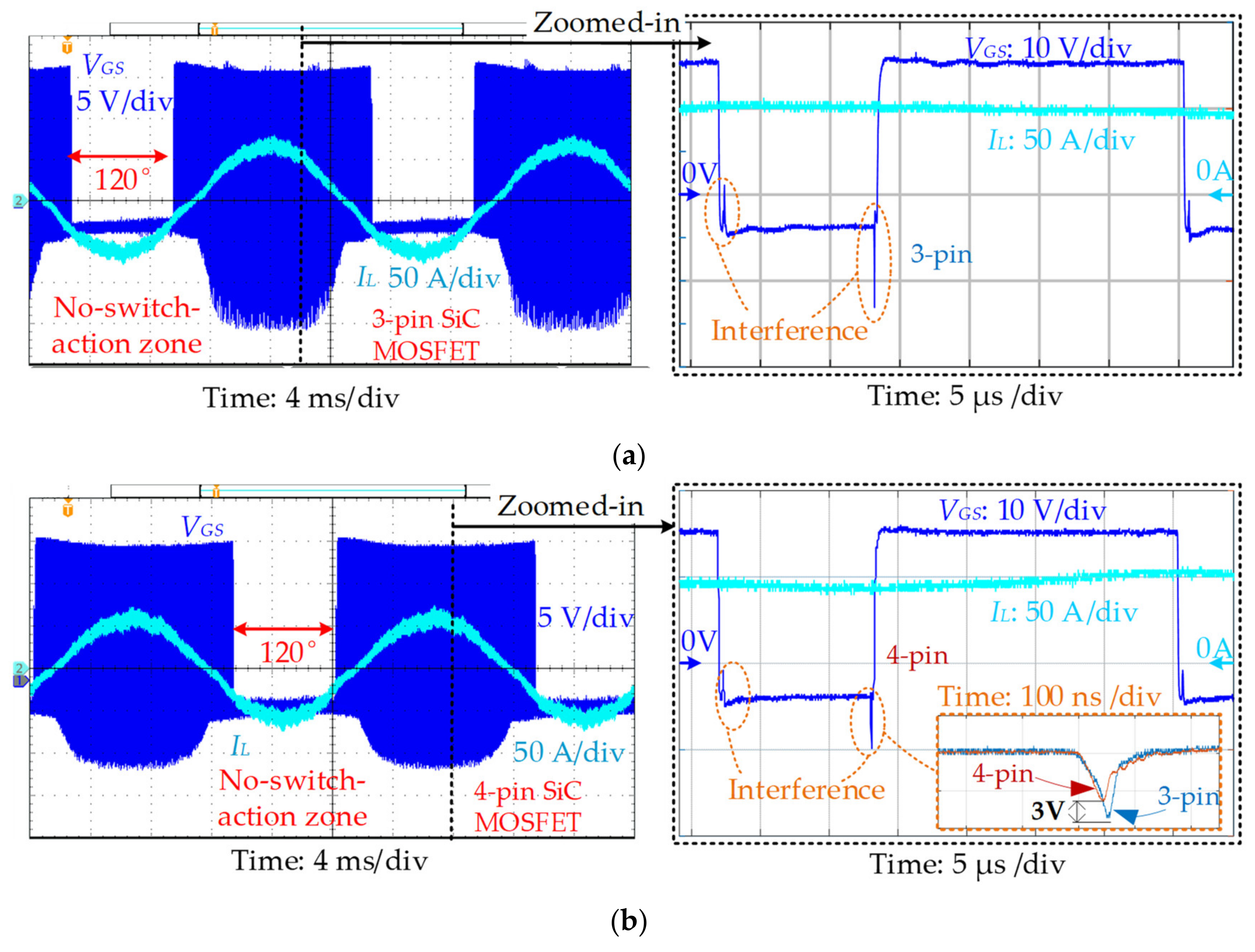
Figure 8 shows the experiment result of the PWM rectifier at 30 kW, full-load point. VGS is the gate-source voltage of one of the SiC MOSFETs in the rectifier. Moreover, IL is the current of its filter inductance, which is also the input AC current. The prototype adopted the optimized SVPWM method, with a 120 ° no-switch-action zone shown on the VGS waveform. Figure 8a shows the waveforms from the 3-pin version of the PWM rectifier, and Figure 8b shows the waveforms from the 4-pin version.
Both the 3-pin version and the 4-pin version operated as designed, as given on the left of Figure 8a,b. On the right side, the zoomed-in areas of the waveforms show the details of the gate-source voltage VGS. After the falling edge, the VGS waveform showed a positive spike interference; Before the rising edge, the VGS waveform showed a negative spike interference. In Figure 8b, we took the negative spike as an example to further zoom-in and compared it with the 3-pin version’s VGS waveform. The waveform showed about 3 V decreased spike, at this time point, by using 4-pin packaged SiC MOSFETs.
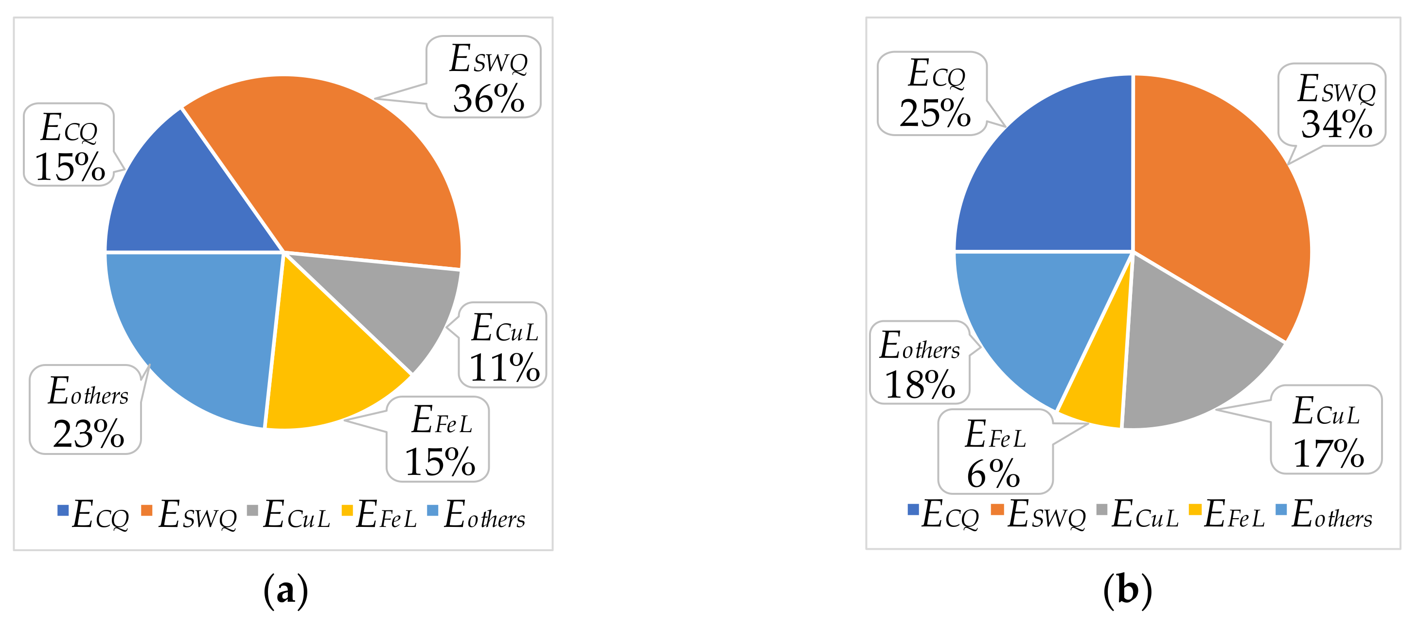
The loss distribution of 3-pin version all-SiC PWM rectifier is shown in Figure 9. The switching loss of the SiC MOSFETs accounted for the most significant proportion of the total loss, over 1/3, both at full-load 30 kW and half-load 15 kW. Etot is the total loss of PWM rectifier, and P is the operation power. At half-load, the total loss shared 2.2% of the operation power. At full-load, the total loss shared 2.6% of the operation power. The share of switching loss was 42% at half-load and 36% at full-load.
The technical parameters used in the 4-pin SiC MOSFETs PWM rectifier were consistent with 3-pin SiC MOSFETs PWM rectifier, as shown in Table 2. Moreover, the loss distribution of the 4-pin SiC MOSFETs PWM rectifier is shown in Figure 10. Like the 3-pin version, the switching loss of the SiC MOSFETs accounted for the most significant proportion of the total loss, over 1/3, both at full-load 30 kW and half-load 15 kW. Meanwhile, the portion of switching loss was less than that of the 3-pin version. The share of switching loss was 36% at half-load and 34% at full-load.
Figure 9 and Figure 10 represent the loss distribution of the two versions of PWM rectifiers, and they were generated with the loss model mentioned above. Although the values we used in the model had a certain level of uncertainty with the real value, which mainly caused by the value’s non-linearity in rectifiers application, the results are practicable to explain the loss variation trends. It could be obtained from Figure 9 and Figure 10:
  • The switching loss was more than 1/3 of total loss at half-load and full-load conditions for all-SiC PWM rectifiers, and it had become the crucial factor for the efficiency.
  • The PWM rectifier using the 4-pin SiC MOSFETs had a reduced total loss under 15 kW and 30 kW conditions than 3-pin SiC MOSFETs. The loss was reduced by about 0.2% at 15 kW and about 0.1% at 30 kW.
  • The switching loss proportion of 4-pin SiC MOSFETs PWM rectifier was less than 3-pin SiC MOSFETs (6% less at 15 kW and 2% less at 30 kW).
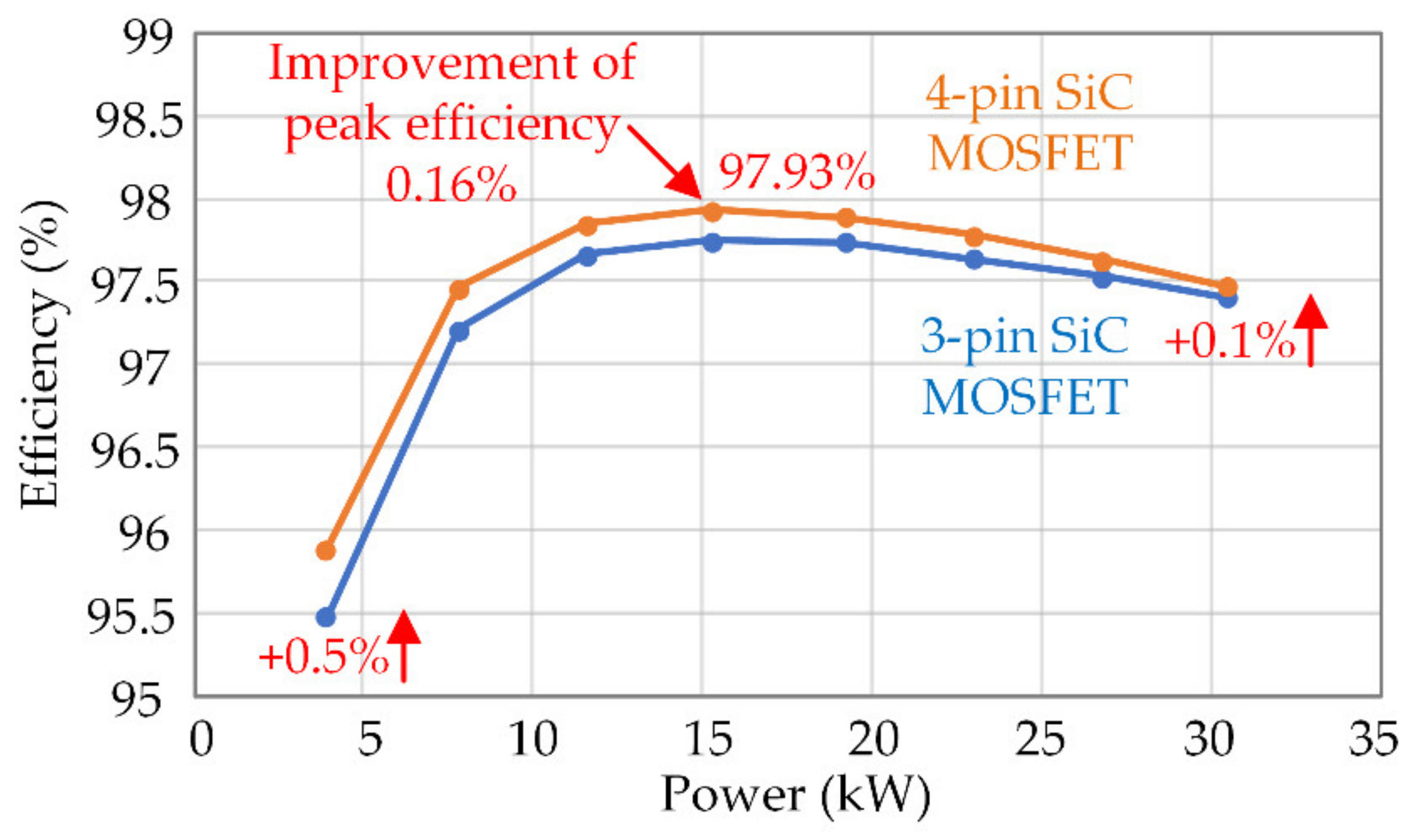
Figure 11 was obtained by measuring the efficiency of 3-pin and 4-pin SiC MOSFET PWM rectifiers, including the cooling fans and auxiliary power supply (APS), at different power conditions, ranged from light-load to full-load. The experimental results showed the efficiency improvement, introducing 4-pin Kelvin package SiC MOSFETs. The efficiency was increased by about 0.5% (20 W) at 4 kW, and the efficiency was increased by about 0.1% (30 W) at 30 kW at full-load. The peak efficiency, using 4-pin SiC MOSFET, was as high as 97.93%, which was 0.16% higher than the peak efficiency of the 3-pin-based PWM rectifier.

6. Conclusions

For the fast EV charging application, this paper considered the impact of gate-source voltage interference on the power loss, revealing an efficiency optimization for all-SiC PWM rectifiers. It introduced theoretical analysis and experimental verification to investigate efficiency optimization, using 4-pin Kelvin packaged SiC MOSFETs. The obtained results are summarized as follows:
  • The rapid change of the main power current (di/dt) induced an electromotive force on the source parasitic inductance of the 3-pin SiC MOSFET, which was opposite to the driving voltage, suppressing the gate-source voltage change and increasing the switching loss.
  • The mechanism of improving system efficiency by using the 4-pin Kelvin packaged SiC MOSFETs was theoretically investigated. The drive circuit of SiC MOSFETs could be approximately equivalent to a second-order system, and the switching time could be derived. Moreover, the switching time of 4-pin SiC MOSFETs was theoretically less than that of general 3-pin SiC MOSFETs.
  • The loss model of all-SiC PWM rectifier was established by considering the impact of gate-source voltage interference. The switching loss of 4-pin SiC MOSFETs was smaller than 3-pin SiC MOSFETs, so the total loss of the PWM rectifier was decreased, and the system efficiency was improved.
  • Based on the industrial product case study, two 30 kW all-SiC PWM rectifier versions were investigated, using 3-pin SiC MOSFETs and 4-pin SiC MOSFETs, respectively. The switching loss was more than 1/3 of the total loss for both of the rectifiers. However, the switching loss proportion of 4-pin SiC MOSFETs PWM rectifier was less than 3-pin SiC MOSFETs (6% less at 15 kW and 2% less at 30 kW).
  • 4-pin Kelvin package SiC MOSFETs improved the efficiency of the PWM rectifier. Experiment results showed that the efficiency was increased by about 0.5% (20 W) maximally at 4 kW, and about 0.1% (30 W) at 30 kW full-load. The peak efficiency of the PWM rectifier, using 4-pin SiC MOSFETs, was as high as 97.93%, which was 0.16% higher than the peak efficiency of the 3-pin SiC MOSFETs-based PWM rectifier.
The research of this paper would provide a valuable reference for the industrial application of SiC semiconductors in the power electronics area.

Author Contributions

Conceptualization, Z.L. and T.S.; data curation, Z.W.; formal analysis, Z.W.; funding acquisition, H.L.; investigation, T.S.; methodology, Z.W., T.Z., and H.L.; project administration, Z.L.; resources, Z.L.; software, B.H.; supervision, T.Z.; validation, Z.L., B.H., and T.S.; visualization, H.L.; writing–original draft, Z.L.; writing–review and editing, T.S. All authors have read and agreed to the published version of the manuscript.

Funding

This work was supported in part by the Excellent Youth Scholars of National Natural Science Foundation of China under Grant 51822701, in part by the Key Project of National Natural Science Foundation of China under Grant U1866211.

Conflicts of Interest

The authors declare no conflict of interest.

References

  1. Li, F.; Zhang, X.; Zhu, H.; Li, H.; Yu, C. An LCL-LC Filter for Grid-Connected Converter: Topology, Parameter, and Analysis. IEEE Trans. Power Electron. 2014, 30, 5067–5077. [Google Scholar] [CrossRef]
  2. Shao, T.-C.; Jia, P.; Zheng, P.-Q.; Zheng, T.Q.; Wang, J.; Li, H.; Liang, M.; Zhang, X. A Robust Power Regulation Controller to Enhance Dynamic Performance of Voltage Source Converters. IEEE Trans. Power Electron. 2019, 34, 12407–12422. [Google Scholar] [CrossRef]
  3. Wang, H.; Mingli, W.; Sun, J.; Wu, M. Analysis of Low-Frequency Oscillation in Electric Railways Based on Small-Signal Modeling of Vehicle-Grid System in dq Frame. IEEE Trans. Power Electron. 2015, 30, 5318–5330. [Google Scholar] [CrossRef]
  4. Song, K.; Mingli, W.; Yang, S.; Liu, Q.; Agelidis, V.G.; Konstantinou, G.; Wu, M. High-Order Harmonic Resonances in Traction Power Supplies: A Review Based on Railway Operational Data, Measurements, and Experience. IEEE Trans. Power Electron. 2020, 35, 2501–2518. [Google Scholar] [CrossRef]
  5. Li, Z.; Shao, T.; Zheng, T.Q.; Li, H.; Huang, B. Interference source analysis and EMC design for All-SiC power module in EV charger. Microelectron. Reliab. 2019, 113458. [Google Scholar] [CrossRef]
  6. Papamanolis, P.; Krismer, F.; Kolar, J.W. 22 kW EV Battery Charger Allowing Full Power Delivery in 3-Phase as well as 1-Phase Operation. In Proceedings of the 10th International Conference on Power Electronics and ECCE Asia (ICPE 2019—ECCE Asia), Busan, South Korea, 27–30 May 2019; pp. 1–8. [Google Scholar]
  7. Wang, F.; Zhang, Z.; Ericsen, T.; Raju, R.; Burgos, R.; Boroyevich, D. Advances in Power Conversion and Drives for Shipboard Systems. Proc. IEEE 2015, 103, 2285–2311. [Google Scholar] [CrossRef]
  8. Hamada, K.; Nagao, M.; Ajioka, M.; Kawai, F. SiC—Emerging Power Device Technology for Next-Generation Electrically Powered Environmentally Friendly Vehicles. IEEE Trans. Electron Devices 2014, 62, 278–285. [Google Scholar] [CrossRef]
  9. Karacolak, T.; Thirumalai, R.V.K.G.; Merrett, J.N.; Koshka, Y.; Topsakal, E. Silicon Carbide (SiC) Antennas for High-Temperature and High-Power Applications. IEEE Antennas Wirel. Propag. Lett. 2013, 12, 409–412. [Google Scholar] [CrossRef]
  10. Larry, S.; Lucas, L. Silicon, GaN and SiC: There’s Room for All—An application space overview of device considerations. In Proceedings of the 30th International Symposium on Power Semiconductor Devices and ICs, Chicago, IL, USA, 13–17 May 2018; pp. 8–11. [Google Scholar]
  11. Chow, T.P. Wide Bandgap Semiconductor Power Devices for Energy Efficient Systems. In Proceedings of the IEEE 3rd Workshop on Wide Bandgap Power Devices and Applications (WiPDA), Blacksburg, VA, USA, 2–4 November 2015; pp. 400–405. [Google Scholar]
  12. Bindra, A. Wide-Bandgap-Based Power Devices: Reshaping the power electronics landscape. IEEE Power Electron. Mag. 2015, 2, 42–47. [Google Scholar] [CrossRef]
  13. Danan, Y.; Ilovitsh, T.; Ramon, Y.; Malka, D.; Liu, D.; Zalevsky, Z. Silicon-coated gold nanoparticles nanoscopy. J. Nanophotonics 2016, 10, 36015. [Google Scholar] [CrossRef]
  14. Samoi, E.; Benezra, Y.; Malka, D. An ultracompact 3 × 1 MMI power-combiner based on Si slot-waveguide structures. Photonics Nanostructures Fundam. Appl. 2020, 39, 100780. [Google Scholar] [CrossRef]
  15. Malka, D.; Berke, B.A.; Tischler, Y.; Zalevsky, Z. Improving Raman spectra of pure silicon using super-resolved method. J. Opt. 2019, 21, 075801. [Google Scholar] [CrossRef]
  16. Zhang, W.; Huang, X.; Lee, F.C.; Li, Q.I. Gate drive design considerations for high voltage cascode GaN HEMT. In Proceedings of the IEEE Applied Power Electronics Conference and Exposition—APEC, Fort Worth, TX, USA, 16–20 March 2014; pp. 1484–1489. [Google Scholar]
  17. Analog Devices Inc. Design Fundamentals of Implementing an Isolated Half-Bridge Gate Driver. Available online: https://www.analog.com (accessed on 18 March 2020).
  18. Liu, P.; Guo, S.; Yu, R.; Huang, A.Q.; Zhang, L. Analysis of Trade-Off Between Noise and Wide Band-Gap (WBG) Device Switching Speed. In Proceedings of the IEEE Energy Conversion Congress and Exposition (ECCE), Portland, OR, USA, 23–27 September 2018; pp. 3483–3489. [Google Scholar]
  19. Zhang, Z.; Zhang, W.; Wang, F.; Tolbert, L.M.; Blalock, B.J. Analysis of the switching speed limitation of wide band-gap devices in a phase-leg configuration. In Proceedings of the IEEE Energy Conversion Congress and Exposition (ECCE), Raleigh, NC, USA, 15–20 September 2012; pp. 3950–3955. [Google Scholar]
  20. Zhang, Z.; Wang, F.; Tolbert, L.M.; Blalock, B.J. Active Gate Driver for Crosstalk Suppression of SiC Devices in a Phase-Leg Configuration. IEEE Trans. Power Electron 2014, 29, 1986–1997. [Google Scholar] [CrossRef]
  21. Zhang, Z.; Dix, J.; Wang, F.F.; Blalock, B.J.; Costinett, D.; Tolbert, L.M. Intelligent Gate Drive for Fast Switching and Crosstalk Suppression of SiC Devices. IEEE Trans. Power Electron. 2017, 32, 9319–9332. [Google Scholar] [CrossRef]
  22. STMicroelectronics Mitigation technique of the SiC MOSFET gate voltage glitches with Miller clamp. Available online: https://www.st.com (accessed on 18 March 2020).
  23. Burkart, R.M.; Kolar, J.W. Comparative evaluation of SiC and Si PV inverter systems based on power density and efficiency as indicators of initial cost and operating revenue. In Proceedings of the IEEE 14th Workshop on Control and Modeling for Power Electronics (COMPEL), Salt Lake City, UT, USA, 23–26 June 2013; pp. 1–6. [Google Scholar]
  24. Burkart, R.M.; Kolar, J.W. Comparative Life Cycle Costs Analysis of Si and SiC PV Converter Systems Based on Advanced η-ρ-σ Multi-Objective Optimization Techniques. IEEE Trans. Power Electron. 2017, 32, 4344–4358. [Google Scholar] [CrossRef]
  25. Burkart, R.M.; Kolar, J.W. Comparative η-ρ-σ Pareto Optimization of Si and SiC Multilevel Dual-Active-Bridge Topologies With Wide Input Voltage Range. IEEE Trans. Power Electron. 2017, 32, 5258–5270. [Google Scholar] [CrossRef]
  26. Xie, R.; Wang, H.; Tang, G.; Yang, X.; Chen, K.J. An Analytical Model for False Turn-On Evaluation of High-Voltage Enhancement-Mode GaN Transistor in Bridge-Leg Configuration. IEEE Trans. Power Electron. 2017, 32, 6416–6433. [Google Scholar] [CrossRef]
  27. Ren, Y.; Xu, M.; Zhou, J.; Lee, F. Analytical loss model of power MOSFET. IEEE Trans. Power Electron. 2006, 21, 310–319. [Google Scholar]
  28. Trzynadlowski, A.; Kirlin, R.; Legowski, S. Space vector PWM technique with minimum switching losses and a variable pulse rate [for VSI]. IEEE Trans. Ind. Electron. 1997, 44, 173–181. [Google Scholar] [CrossRef]
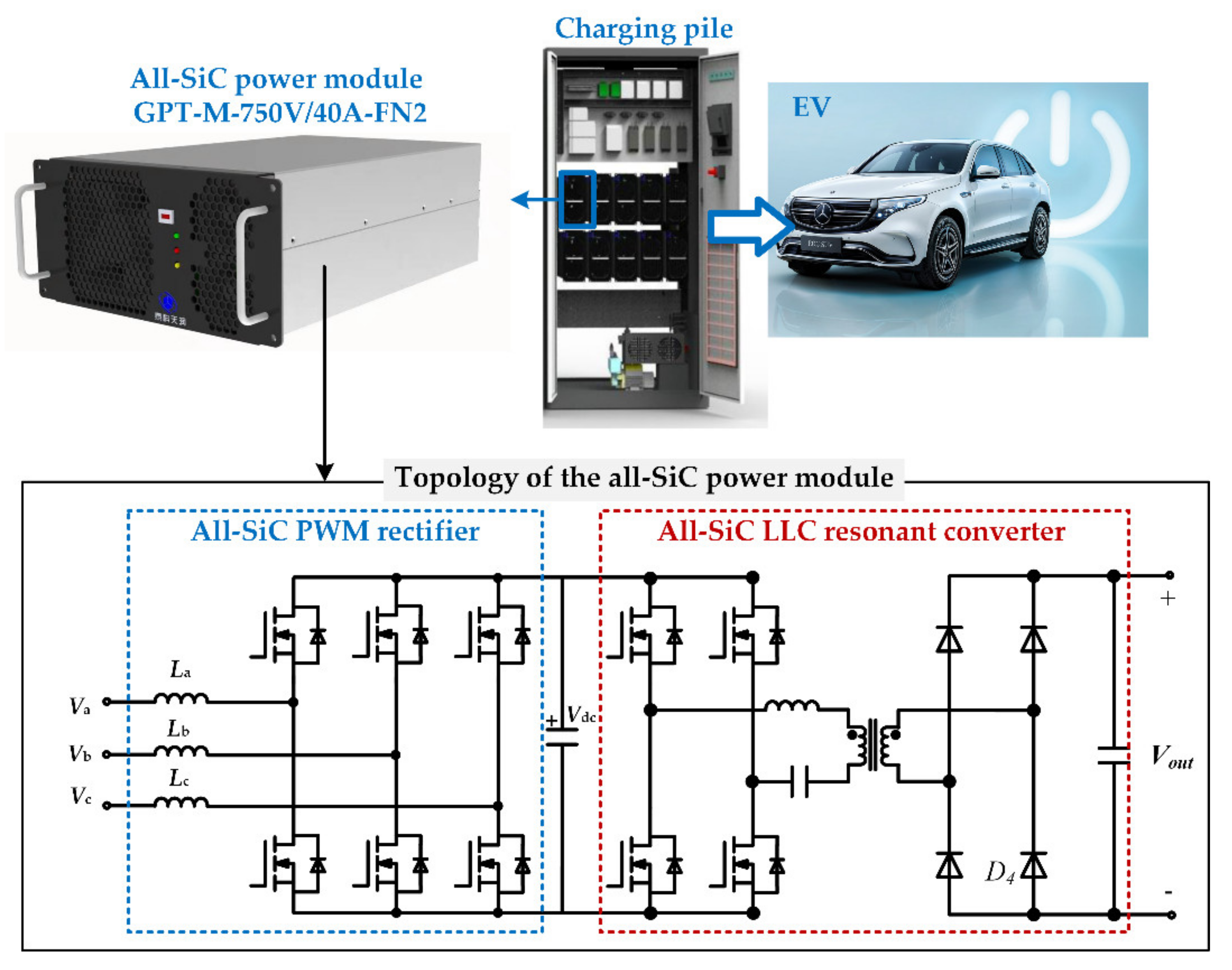
Figure 1. The outlook of the electric vehicle (EV) charging pile and the topological diagram of its all-SiC (silicon carbide) power module with the Pulse Width Modulation (PWM) rectifier.
Energies 13 01421 g001
Figure 2. Framework diagram of all-SiC power module system with PWM rectifier inside.
Energies 13 01421 g002
Figure 3. The parasitic parameters of the bridge circuit and its driving circuit: (a) 3-pin SiC Metal-Oxide-Semiconductor Field-Effect Transistor (MOSFET), (b) 4-pin SiC MOSFET.
Energies 13 01421 g003
Figure 4. The current flow of general 3-pin SiC MOSFET during switching: (a) Turn-on process, (b) Turn-off process.
Energies 13 01421 g004
Figure 5. The simplified waveforms change during SiC MOSFET switching: (a) Turn-on process, (b) Turn-off process.
Energies 13 01421 g005
Figure 6. The current flow of general 4-pin SiC MOSFET during switching: (a) Turn-on process, (b) Turn-off process.
Energies 13 01421 g006
Figure 7. Experimental device for all-SiC MOSFET PWM rectifier.
Energies 13 01421 g007
Figure 8. The experiment result of the all-SiC PWM rectifier: (a) 3-pin version, (b) 4-pin version.
Energies 13 01421 g008
Figure 9. Loss distribution diagram of 3-pin all-SiC MOSFET PWM rectifier: (a) Half-load 15 kW (Etot/P≈2.2%), (b) Full-load 30 kW (Etot/P≈2.6%).
Energies 13 01421 g009
Figure 10. Loss distribution diagram of 4-pin all-SiC MOSFET PWM rectifier: (a) Half-load 15 kW (Etot/P≈2.0%), (b) Full-load 30 kW (Etot/P≈2.5%).
Energies 13 01421 g010
Figure 11. Efficiency curve of the all-SiC PWM rectifier.
Energies 13 01421 g011
Table 1. Technical specifications of the all-SiC (silicon carbide) power module.
TermsContentTermsContent
Basic IndexOutput Characteristic
Size133 mm (H) × 242 mm (W) × 395 mm (D)Rated voltage750 VDC
Weight≤ 15.5 kgRated current40 A
Operation temperature−25 °C ~ + 75 °C
−25 °C ~+ 65 °C fully output
+65 °C ~ + 75 °C limited output
Max. current50 A
Storage temperature−40 °C ~ + 75 °CVoltage range300 V ~ 750 V
Relative humidity5% RH ~ 95% RH (no condensation)Max. power30 kW
Altitude≤2000 m (limited function over 2000 m)Voltage accuracy≤ ± 0.5%
Cooling modeIntelligent air coolingCurrent accuracy≤ ± 1%
Communication bus protocolCANCurrent error≤ ± 0.5%
Max. NO. for parallel 32Voltage error≤ ± 1%
Input CharacteristicOutput ripplePeak coefficient < 1%
Root Mean Square (RMS) coefficient < 0.5%
Operation voltage270 VAC ~ 450 VAC
270 VAC ~ 320 VAC limited output; 320 VAC ~ 450 VAC fully output
Starting impulse current≤ 110%
Frequency45 Hz ~ 65 Hz, 50 Hz/60 Hz ratedPeak efficiency≥ 97%
Input current≤ 60 ABoot time3 s ~ 8 s
Power factor≥ 0.98 (loaded rate 50% ~ 100%)Noise< 65 dB (measurement distance 1 m)
Current THD≤ 5% (loaded rate 50% ~ 100%)Stand-by loss≤ 25 W (380 VAC input)
Table 2. Pulse Width Modulation (PWM) rectifier components.
ComponentManufacturerModelParameters
3-pin SiC MOSFETGlobal Power TechnologyGIM040120B1200 V 40 mΩ
4-pin SiC MOSFETGlobal Power TechnologyGIM040120E1200 V 40 mΩ
AC side inductance225 μH
Table 3. Rated parameters of the PWM rectifier.
ParameterValueUnitNote
Rated power30kW
AC voltage380VThree-phase
DC voltage750V
Switching Frequency30kHz
AC side inductance225μH225 μH