Article

An Optimal Control Scheme for Load Bus Voltage Regulation and Reactive Power-Sharing in an Islanded Microgrid

1
School of Electrical and Information Engineering, Tianjin University, Tianjin 300072, China
2
Department of Electrical and Computer Engineering, COMSATS University Islamabad, Lahore 54000, Pakistan
3
College of Energy and Electrical Engineering, Hohai University, Nanjing 211100, China
4
Department of Electrical Engineering, University of Engineering and Technology, Lahore 54890, Pakistan
5
Department of Electrical Engineering, College of Engineering, Jouf University, Sakaka 72388, Saudi Arabia
6
Department of Electrical Engineering, Faculty of Engineering, Aswan University, Aswan 81542, Egypt
7
Engineering and Applied Sciences Research Unit, Jouf University, Sakaka 72388, Saudi Arabia
*
Authors to whom correspondence should be addressed.
Energies 2021, 14(20), 6490; https://doi.org/10.3390/en14206490
Submission received: 23 August 2021 / Revised: 25 September 2021 / Accepted: 30 September 2021 / Published: 10 October 2021
(This article belongs to the Section F: Electrical Engineering)

Abstract

:
This paper presents an optimal control scheme for an islanded microgrid (MG), which performs reactive power-sharing and voltage regulation. Two-fold objectives are achieved, i.e., the load estimation strategy, firstly, approximates the MG’s impedance and transmits this information through a communication link. Based on approximated impedance information, an optimal regulator is then constructed to send optimal control commands to respective local power controllers of each distributed generation unit. An optimal regulator is a constraints optimized problem, mainly responsible to restore the buses’ voltage magnitudes and realize power-sharing proportionally. The important aspect of this control approach is that the voltage magnitude information is only required to be transferred to each inverter’s controller. In parallel, a secondary control layer for frequency restoration is implemented to minimize the system frequency deviations. The MATLAB/Simulink and experimental results obtained under load disturbances show the effectiveness for optimizing the voltage and power. Modeling and analysis are also verified through stability analysis using system-wide mathematical small-signal models.

1. Introduction

One of the important factors of autonomous MG is to drive the electrical network with high security and reliability at various operating conditions. Control of voltage and reactive power is a salient step in order to obtain a reliable smart network [1,2,3]. Such issues have been investigated by many researchers as it is considered one of the leading cause for voltage collapse, which may drive the power system blackout [4]. Voltage vulnerability can be defined as the failure of bus voltage to return at a nominal value under disturbance [5,6]. Most of the power shutdown came about from voltage uncertainty, which predominantly came up due to failure of the control system to draw out adequate reactive power to reinforce the voltage at fault-finding grid buses [7]. The issue principally emerged from depending on an on–off control facility, without using an automatic control system. The design of voltage control and the power-sharing layer was first set up by European countries and later propagated by the United States, Asia, and Africa, respectively [4]. Each country employed the control layers in accordance with their own methodology, which is sufficient to remove the voltage fluctuations and well address the reactive power sharing.
Three hierarchical control loops use to control the voltage and power sharing in islanded smart grids, i.e., primary, secondary, and tertiary controls layers [8,9,10,11]. The primary layer restores the autonomous MGs voltage magnitude while the secondary control is responsible for regulating the load buses voltage magnitude within an acceptable range. Wherein, the tertiary voltage control addresses the setting values of the pilot bus based on optimal power flow. The droop control schemes are widely used to obtain the power-sharing by using a communication channel. Power-sharing control schemes of DG units, based on communication, are master/slave [12,13], concentrated control [14,15], and distributed control [16,17]. In contrast, the control methodologies without using the communication channel are mainly based on the droop idea, which includes four leading categories: (1) virtual framework structure-based scheme [18,19,20,21,22,23]; (2) signal injection strategy [24]; (3) conventional and variants of the droop control [10,25,26,27,28,29]; (4) “construct and compensate” based schemes [15,30,31].
The real power-frequency p-f and reactive power-voltage Q-V droop layers are employed to resolve the power control issues [6,32,33,34,35]. Authors presented an improved power sharing control strategy to regulate the load bus voltage but at the cost of inverter terminal voltage deviation [27]. A “Q-V dot droop” scheme was developed but the reactive power sharing was not evident when the local loads were added [36]. The droop control schemes based on virtual impedance are observed as an evident strategy to deal with reactive power-sharing problems [30,31,37,38]. The power sharing can be improved by virtual impedance techniques, but voltage droop and virtual impedance deteriorate the inverter terminal voltage quality [39,40]. Voltage control methods are presented in [35] in order to reduce the trade-off between bus voltage and reactive power. Such schemes develop additional voltage offset for compensation by depending on the communication link, which may lead to voltage instability due to time delay. A distributed voltage control scheme is developed to regulate system voltage without a communication link, but the reactive power-sharing performance has not. Recently, a Kalman filter-based state estimator scheme was used for reactive power sharing and bus voltage regulation, however, this strategy requires a high bandwidth data rate and thus increases complexity when generation units are located at long distances [41,42].
Power systems are predominantly working under stressed operating conditions due to speedy growing load demand. The voltage stability has set off vital concerns in present-day electrical power system operations which depends on the proportional realization of reactive power. Even the simplest version of the distribution system faces challenges such as load bus voltage restoration and at the same time minimizing the circulating reactive power in grid-forming nodes. Therefore, in this paper, an effort has been made to resolve such issues faced by an islanded MG distribution network. To the best of our knowledge, the simple quadratic optimized cost function-based techniques for optimizing the load bus voltage and power are not fully investigated and further research is required to enhance the existing studies. In some articles, various methods have been sought to achieve these aims by acquiring real-time signals at each load bus, however, it overburdens communication by taking up high communication bandwidth. On that account, this paper presents an optimal control method, an extension of previous work [34]. The presented method does not require accurate grid impedance information, eventually reduces the data bandwidth. We summarize the major contribution of this work as follows:
  • This study is conducted in a radial feeder system accompanied by three load buses connected with two grid forming nodes.
  • The approximated impedance information of all load-buses is estimated through local load agents, which reduces the bandwidth data requirement.
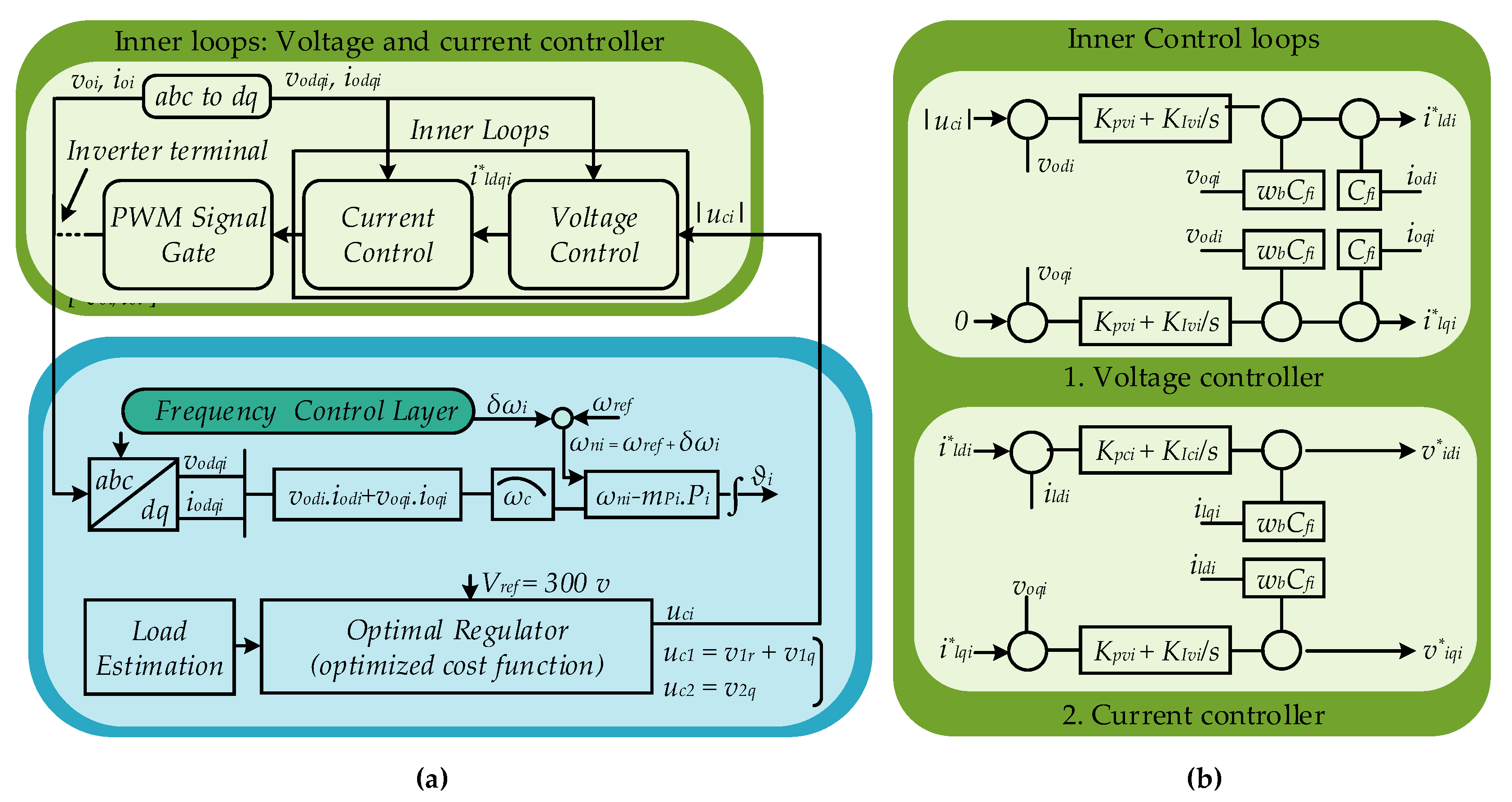
  • An optimal regulator, an optimized cost function, is constructed to send optimal control commands to the inner layer of each DG unit. Moreover, the secondary control layer is responsible to restore the frequency deviations.
  • The MATLAB/Simulink (R2018a, product registered with TJU, China) and experiment results show the effectiveness of the proposed methodology. For the stability analysis, separate Simulink and a linear analysis tool are considered to analyze the complex system by perturbing dynamical equations of the same.
The remainder of this paper is organized as follows. Section 2 presents the design procedure with details of the system used in the proposed study. Section 3 outlines the operation principle of the proposed optimal control strategy. Section 4 provides the derivations of the small-signal model for this MGs system with the employed controls. Section 5 elaborates the stability analysis of the system under the discussed controls. Further, it also presents the simulation and experimental results in detail with and without the proposed control scheme, and finally, Section 6 concludes the paper.

2. Design Procedure

This section details the general procedural design flow of the proposed methodology, which is primarily composed of load estimation and an optimal regulator, illustrated by Figure 1. In the load estimation strategy, the load impedance of ith (i = 1, 2, 3) bus is calculated through measured voltage and current at each bus node. Based on such impedance information, the grid impedance is approximated in terms of one node, as discussed in detail in Section 3.1. An optimal regulator sends the control commands uci (uc1, uc2) to inner control layers, according to the received approximated grid impedance information. To adequately describe the problem and presented technique, we now systematically go about describing the mechanism of optimizing power and voltage, power flow control, and power steady-state equations with the necessary mathematical representations.

3. Proposed Optimal Control Strategy

This section describes the operation principle of the proposed methodology and details the associated MG setup employed in this research. For simulation studies, a radial type of feeder is used as shown in Figure 2, where two DG units are interfaced using three phase, three-wire power electronics inverters, feeding three load buses Vbus1, Vbus2, and Vbus3 through feeder impedances with connected loads, i.e., Zload1, Zload2, and Zload3. The working principle of load estimation and an optimal regulator is discussed in Section 3.1 and Section 3.2, respectively. System control parameters for the stability analysis, simulation, and experiment are given in Table 1 and Table 2.

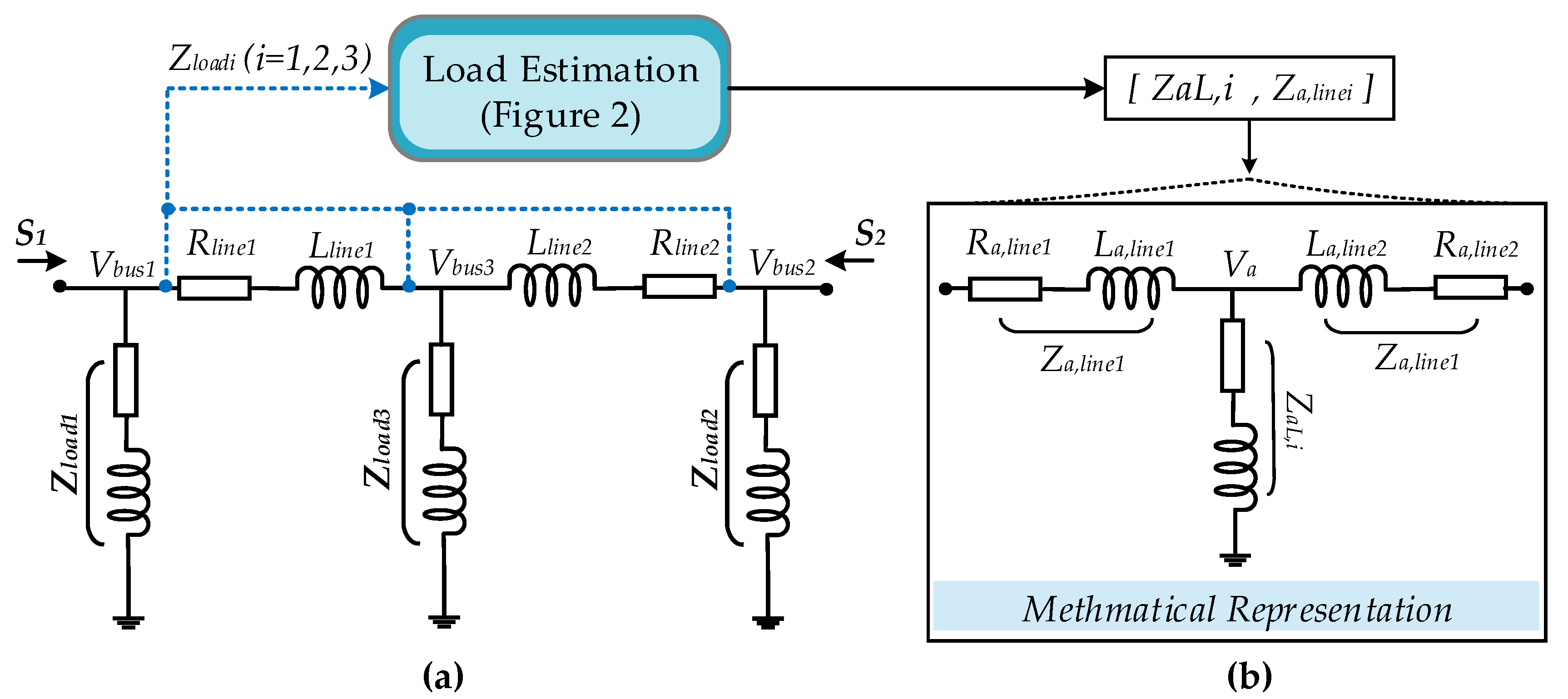
3.1. Load Estimation: The Approximation of Grid Impedance

The load estimation strategy does not require the accurate grid impedance information of each load bus, as the computational complexity increases proportional to the number of load buses. In this presented study, three load buses connected in a radial configuration are considered, as illustrated in Figure 3. The technique, firstly sense the voltage Vbus and current Ibus at each local load node. Sinus-based park transformation is then employed from measured three-phase signals to a dq0 rotating reference frame. The angular position of the rotating frame is given by input ϑi in rad/s, which vary from 0 to 2π. Deduce the dq0 components from three-phase bus voltage signal by performing Clarke transformation, yields vs = (vd + j.vq) = (vα + j.vβ).ej(ϑit−π/2) and vdqo = Kptv.vabc, where, vdq0 = [vd vq v0] t and vabc = [va vb vc] t. The term Kpv denotes the park transformation matrix as given in Appendix A. The dq0 components are expressed as:
v c = v d ± j v q
Similarly, deduce the dq0 components from every ith (i = 1, 2, 3) load current, results is = (id + j.iq) = (iα + j.iβ).ej(ϑit−π/2) and idqo = Kpti.iabc, where, idq0 = [id iq i0]t and iabc = [ia ib ic]t. The dq0 components of idq0 is written as:
i c = i d ± j i q
The load impedance information of the ith bus (i = 1, 2, 3) is estimated by the ratio of Equation (1) to Equation (2), yielding:
Z l o a d i = ( v d ± j v q ) / ( i d ± j i q ) Z l o a d i = Z r e a l i + j Z i m a g i
Once the load impedance of each bus is estimated through local node agents, then the impedance approximation procedure is adopted, expressed by Equations (4)–(7), and illustrated in Figure 3. Wherein, the two optimal control commands uci (uc1, uc2) are the voltage inputs to the inner control layers of DG1 and DG2, as discussed in detail in Section 3.2. For the simulation studies, uc1 of DG1 has been considered as variable frequency while uc2 of DG2 only voltage magnitude is used. Knowing the parameters, e.g., Si, load bus impedance Zloadi (i = 1,2,3), and optimal control commands uci (i = 1,2), we can now approximate the three load buses impedances in term of 1 load node as a mathematical representation depicted in Figure 3.
u i = v i r + v i q ;   u ( i + 1 ) = v ( i + 1 ) r
Z a L , i = [ i = 1 i = 3 1 Z l o a d i ] 1
i i = c o n j ( 2 S i u c i )
V a L i n e , i = u c i [ c o n j ( 2 * S i u c i ) . [ i = 1 i = 3 1 Z l o a d i ] 1 ] Z a L i n e , i = u c i [ c o n j ( 2 * S i u c i ) . [ i = 1 i = 3 1 Z l o a d i ] 1 ] / i i
Where, the ZaLine,i (ZaLine,1, ZaLine,2) and ZaL,i (I = 1) are the approximated transmission lines and load impedances, respectively. Once the grid impedances are approximated then the optimal regulator, discussed in Section 3.2, is constructed to compute the control commands based on received impedance information.

3.2. Optimal Regulator and Algorith Flowchart

The proposed optimal regulator, an equality optimized cost function, computes control commands according to MG’s approximated load impedance information. To minimize cost of function, different optimization techniques are being employed, e.g., linear, quadratic, and higher-order optimization methods. Solvability of linear optimization is easier, but it only works with linear variables and its problem formulation is peculiar. The solutions of higher-order cost functions are inconvenient. Therefore, in this study, a constraints quadrative optimization problem is considered which is convenient for problem formulation and solvability. Some cost functions have constraints reactive power, i.e., Q1 = Q2 results in a tradeoff between real power and voltage magnitude. Since the reactive power requirement is not stringent, therefore, we considered real power equality constraints, i.e., P1 = P2. The desired control commands are acquired by computing the optimization cost function that minimizes the reactive power sharing error ∆Qi and bus voltage error ∆Vi, expressed by Equation (8).
min   J = ( j = 1 n b ( ω b j ( V b u s j V j r e f ) ) 2 ) + ( ω Q ( Q i Q i + 1 ) ) 2 c o n s t r a i n s t s P i P i + 1 = 0 f o r   i = 1
where ωbj and ωQ are the weights of bus voltage and reactive power error, respectively. The term Vjref = 300 V (j = 1, 2, 3) is the nominal bus voltage, while nb = 3 is the number of load buses that has been chosen for study, as shown in Figure 2.
Figure 4 shows the algorithm flow chart to find the minimum of optimized cost function and is expressed by Equation (9):
Λ ( v 1 r , v 1 q , v 2 r , λ ) = f ( v 1 r , v 1 q , v 2 r ) λ g ( v 1 r , v 1 q , v 2 r )
f ( v 1 r , v 1 q , v 2 r ) = ( j = 1 n b ( ω b j ( V b u s j V j r e f ) ) 2 ) + ( ω Q ( Q i Q i + 1 ) ) 2 λ g ( v 1 r , v 1 q , v 2 r ) = P i P i + 1 = 0
The minima of the augmented function (v1r, v1q, v2r, λ) are located where all of the partial derivatives, i.e., (∂∧/∂v1r = 0, ∧/∂v1q = 0, ∧/∂v2r = 0 and ∧/∂λ = 0) are equal to zero. As the minima “fvalue” of function and control inputs uci, corresponding to different disturbance loads, are illustrated by Figure 4b,c. This algorithm numerically approximates partial derivatives as opposed to analytical evaluation. The important aspect of the numerical derivative strategy is that it can work for multiple variables without even changing the code. Computing the algorithm, the optimal regulator sends the required control commands uci (uc1, uc2) to respective power controllers of the DG units, and the system works the same until the upcoming sampling update. The term uci compensates bus voltage deviation and shares reactive power proportionally. Periodically, the optimal regulator revises its original control plan due to measurements feedback, in line with the latest approximated grid impedance information.

3.3. MG Power Flow Control

The complex power delivered is expressed in terms of network voltages and admittances. Single-phase power relations are utilized as all the quantities are assumed to be in per unit. Therefore, the complex power delivered to the ith bus is written as:
S i = V i ( j = 1 N Y i j V j ) = V i j = 1 N Y i j * V j *
where the term Vi is a phasor term, and the magnitude and angle are expressed by Vi = |Vi|∠φi. The term Yij is the admittance matrix element, define Gij and Bij as the real and imaginary parts, i.e., Yi = Gij + jBij. By applying the algebraic multiplication to Equation (A6), and then collecting the real part Pi and imaginary part Qi, results in:
P i = j = 1 N   | V i | | V j | ( G i j cos ( φ i φ j ) + B i j sin ( φ i φ j ) )
Q i = j = 1 N   | V i | | V j | ( G i j sin ( φ i φ j ) B i j cos ( φ i φ j ) )
Power angle φ in medium voltage lines are small, and we can assume sinφ = φ and cosφ = 1. Therefore, Equations (12) and (13) are re-expressed as:
P i , R x = 0 V i V j X i [ sin φ i j ]
Q i , R x = 0 V i 2 V i V j cos φ i j X i
where φij = XPi/ViVj and ViVj = XQi/Vi. Equations (14) and (15) illustrate a direct relationship among the real power Pi and power angle φ as well as reactive power Qi and voltage magnitude (ViVj).

3.4. Mechanism of Phasor Implementation and Reactive Power Sharing

The output (uc1, uc2) of the proposed optimal regulator is a set of voltage phasors. The direct implementation of voltage phasers of ith inverter in MG requires very fast and reliable communication infrastructure. Nevertheless, in the proposed methodology, the phases have been adjusted through active power and frequency (p-w) droop control loops, only voltage magnitudes are updated in accordance with optimal regulator output. This combination will realize real power proportionally, which is also considered as equality constraint (PiPi+1 = 0) in an optimized cost function, thus the accurate phase angle will be automatically modified by the system.
The real power and frequency (p-ω) droop expression is illustrated by:
ω n i = ω r e f + δ ω i
ω i = ω n i m P i P i
where ωref, and mPi are the nominal frequency and droop coefficients, respectively. The slop of frequency droop characteristic is controlled by mPi parameters. Output frequency of inverter connected with dc power source is adjusted by real power and inner controller. Every ith DG unit is composed in its d-q frame, depending on their angle. By transformation equations, shown in Equation (18), each inverter is transferred to the d-q frame. The proposed power controller is shown in Figure 5a, where the real power and frequency (p-ω) droop layer is responsible for sending the angle to the ith inverter as given by Equation (19).
[ f D f Q ] = [ cos ( ϑ i ) sin ( ϑ i ) sin ( ϑ i ) cos ( ϑ i ) ] [ f d f q ]
ϑ i = ( ω i ) d t
The instantaneous real power (Pi) can be expressed in d-q frame, yields by Pi = (ωc/(s + ωc)) and pi = void. iodi + voqi.ioqi. Here, the term ω c is the cutoff frequency of low pass filters. The vodqi and iodqi are the measured voltage and current in the d-q frame.
Block diagrams of voltage and current control layers are illustrated in Figure 5b. The differential algebraic equations of voltage loop are expressed by:
γ ˙ d i = v o d i * v o d i γ ˙ q i = v o q i * v o q i i l d i * = F i i o d i ± ω b C f i v o d i + K P V i ( v o d i * v o d i ) + K I V i ( v o d i * v o d i ) l q i * = F i i o q i ± ω b C f i v o q i + K P V i ( v o q i * v o q i ) + K I V i ( v o q i * v o q i )
where the term γ ˙ d q i is the auxiliary state variable and wb is the nominal angular frequency. The differential algebraic equations of the current layer are written as:
ζ ˙ d i = i l d i * i l d i ζ ˙ q i = i l q i * i l q i v l d i * = ω b L f i i l d i + K P C i ( i l d i * i l d i ) + K I C i ( i l d i * i l d i ) v l q i * = ω b L f i i l q i + K P C i ( i l q i * i l q i ) + K I C i ( i l q i * i l q i )
where the ζ ˙ d q i is the auxiliary state variable and ildqi are the quadrature components of ili.

3.5. Secondary Layer: The Frequency Restoration Methodology

The aim of the secondary control layer is to observe and minimize the system frequency deviations. The frequency restoration technique is shown in Figure 1 and expressed by,
ω a v g = k = 1 N ω k N δ ω i = ( ω r e f ω a v g ) ]
δ ω i = k p f ( ω r e f ω a v g ) + k i f ( ω r e f ω a v g ) d t
where the terms ωref and ωavg are the nominal and measured frequencies, respectively. The frequency correction term δωi is responsible for regulating the system frequency at scheduled values, i.e., 50 Hz, while Kpf and Ki are the proportional and integral gains, respectively, for controllers.

4. Small Signal Analysis of the MG System

This section details the stability analysis of the system by varying P-w droop gain mPi and communication delay Td. The intermittent latencies and failures of component communication links may result in power imbalances, deviations in voltages, and frequency. For this purpose, we separately considered the MATLAB/Simulink and linear analysis tool to analyze the complex system by perturbing dynamical equations of the same.
The small-signal modeling strategy is based on three important sub-modules, i.e., inverter, network, and loads. State equations of the network and the connected loads with ith DG inverter are presented in the below sections.

4.1. Power Controller

In the proposed methodology, the conventional active power and frequency (P-w) droop layer is used, where the instantaneous power p = vodi.iodi + voqi.ioqi and q = vodi.ioqivoqi.iodi is obtained from the measured voltage and current signals. The small-signal model of active power can be obtained by linearization, yielding:
Δ ˙ P i = ω c i . Δ P i + ω c i ( I o d i Δ v o d i + I o q i Δ v o q i + V o d i Δ i o d i + V o q i Δ i o q i )
where vodqi = [vodi voqi] T and iodqi = [iodi ioqi] T. Since, the traditional reactive power and voltage magnitude (Q-V) droop layer is replaced with “optimal regulator”, as discussed in Section 3.2. Therefore, the state equations for the modified layer of the power controller are described below, accordingly.
The small-signal modeling of optimized cost function approximates complicated multivariable function J near vector inputs V. This task can be achieved more efficiently by quadratic approximation using the information provided by the second partial derivatives as compared to local linearization. The approximation of multi-dimensional input of function J, Equation (9), is expressed by:
Q j ( V ) = j ( V ) + j ( V ) . ( V V ) + 1 2 ( V V * ) T H j ( V ) ( V V )
where j ( V ) , j ( V ) . ( V V ) , and 1 2 ( V V * ) T H j ( V ) ( V V ) are the constant, linear and quadratic terms, respectively. Here, j is the multi-dimensional input with a scalar output function. The term j ( V ) represents the function j gradient which is evaluated at optimal values V*. The gradient of multivariable function j ( v 1 , v 2 ) is presented as sign j , where it contains information of all partial derivate into a vector form, as:
j = [ j v 1 j v 2 ] T
The term H j ( V ) in Equation (25) represents the hessian matrix of function j which is evaluated at V*. The hessian matrix of a multivariable function j ( v 1 , v 2 ) contains all second partial derivatives into a matrix form. The object Hj is no ordinary matrix; it is the matrix with functions evaluated at optimal points ( v 1 , v 2 ) , as represented by:
H j = [ 2 j v 1 * 2 j v 1 v 2 2 j v 2 v 1 2 j v 1 * ]   and   H j ( v 1 * , v 2 * ) = [ 2 j v 1 * ( v 1 * , v 2 * ) 2 j v 1 v 2 ( v 1 * , v 2 * ) 2 j v 2 v 1 ( v 1 * , v 2 * ) 2 j v 1 * ( v 1 * , v 2 * ) ]
The vector V* is the optimal values   [ v 1 *   v 2 * ] T while vector V are the variable inputs which have the same matrix size of vector V*. Finally, perturbation in ∆v1 and ∆v2 with respective to approximated load impedance variation ∆ZL can be achieved, as expressed by Equations (28)–(34), at optimal values of V* and respective load impedance ZLi.
Δ i L i = V s s Z L i 2 Δ Z L i + 1 Δ Z L i Δ V a
Γ 1 ( Δ v 1 , Δ v 2 , Δ Z L i ) =   Q j ( V * , ( Z L i * + Δ Z L i ) v 1
Γ 2 ( Δ v 1 , Δ v 2 , Δ Z L i ) =   Q j ( V * , ( Z L i * + Δ Z L i ) v 2
Δ V = ( H 1 ) * ( V z L Δ z L )
Δ V = [ Δ v 1 Δ v 2 ]
Δ v 1 = [ Δ v 1 * ( cos ( δ s 1 ) + sin ( δ s 1 ) ) ] + [ v i n 1 ( ( sin ( δ s 1 ) Δ δ 1 ) + j v n i 1 ( ( cos ( δ s 1 ) Δ δ 1 ) ] Δ v 2 = [ Δ v 2 * ( cos ( δ s 2 ) + sin ( δ s 2 ) ) ] + [ v i n 2 ( ( sin ( δ s 2 ) Δ δ 2 ) + j v n i 2 ( ( cos ( δ s 2 ) Δ δ 2 ) ]
Δ δ a v g = Δ δ 1 + Δ δ 2 2
where Δ δ 1 = Δ δ 1 Δ δ a v g and Δ δ 2 = Δ δ 2 Δ δ a v g . In Equation (33), the terms vin1 and vin2 are steady-state reference voltages while δs1 and δs2 are the steady-state angle, calculated as
δ s a v g = δ s 1 + δ s 2 2 ;   δ s 1 = δ s 1 δ s a v g   ;   δ s 2 = δ s 2 δ s a v g
Further, the mathematical modeling of gird side filter, complete ith inverter, combined model of N inverters, and network load model are given in Appendix C, Appendix D, Appendix E, and Appendix F, respectively.

4.2. Complete MG Model

The node voltages are used as inputs to every subsystem. In the assurance of a well-defined node voltage, a virtual resistor rN is supposed among every m node and ground; its symbolic form is defined by
[ Δ v b D Q ] = R N ( M I N V [ Δ i o D Q + M l o a d [ Δ i l o a d D Q ] + M N E T [ Δ i l i n e D Q ] )
Diagonal elements of matrix RN are equal to rN with a matrix size of 2 m * 2 m. The mapping matrix MINV and Mload are the size of 2 m ∗ 2 m and 2 m ∗ 2 p, respectively. M NET matrix maps the connecting transmission lines onto the network nodes having a size of 2 m ∗ 2 n. Finally, the complete MG small-signal model is given below.
[ Δ x . i n v Δ i l i n e D Q Δ i l o a d D Q ] = A M G [ Δ x i n v Δ i l i n e D Q Δ i l o a d D Q ]

5. Stability, Simulation, and Experimental Verification

This section details the stability analysis, simulation, and experimental results. The simulations are conducted on MATLAB/Simulink on the circuit configuration shown in Figure 2. Wherein the two paralleled connected DG1 and DG2 units are feeding three load buses. In contrast, the experiments are conducted for three phases, 50 Hz scaled islanded MG prototype as depicted in Figure 6, where the system consists of two identical paralleled DG units with a maximum rating of 3 A, 30 V. Ethernet module USR TCP 232 is used for serial communication transmission of data amongst the data terminal equipment (DTE) and data communication equipment (DCE). The whole platform of islanded MGs is controlled by a desktop LabVIEW control system. The system and controller parameters that have been used for the proposed methodology are given in Table 2.

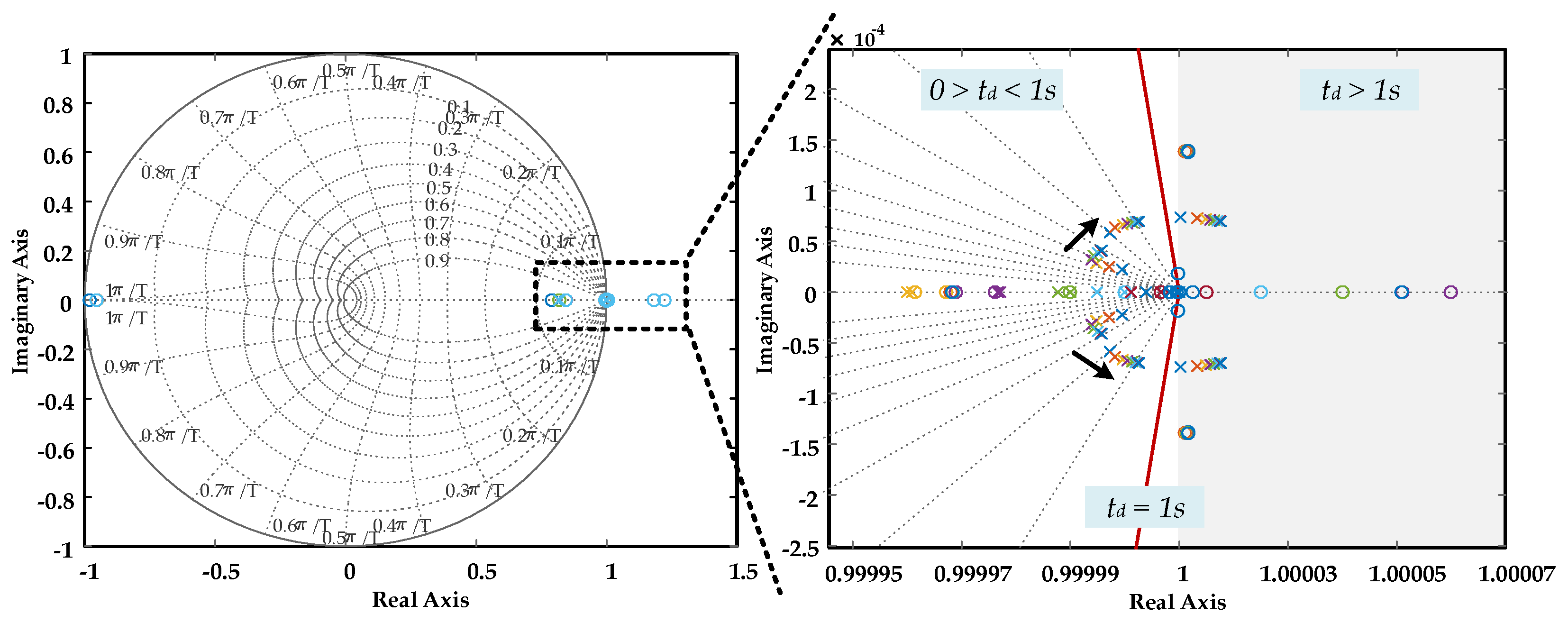
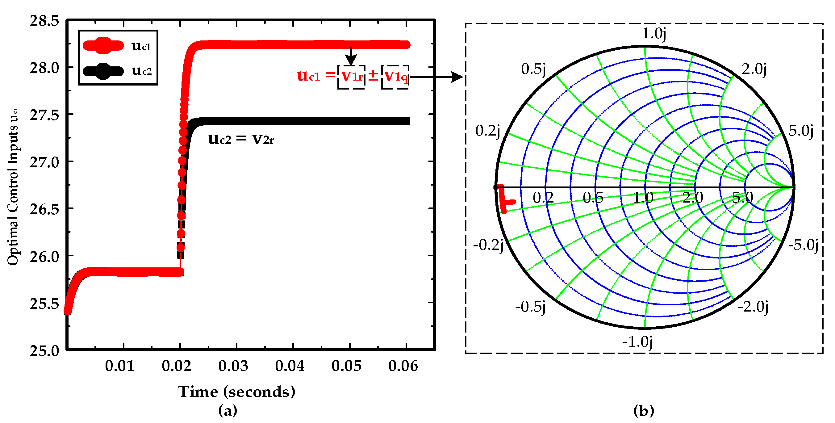
5.1. Stability Analysis Results

The complete model of the test system under the presented control scheme is used to analyze stability under varying communication latencies and control gains. MATLAB/Simulink and linear analysis tools have been used in order to obtain modeling results by analyzing the complex system through perturbing dynamical equations. Figure 7 shows the stability plot for the proposed control framework by varying real power droop gain mP to trace the network trajectory. The control values of the droop gain mP where system poles appear to be in the vicinity of the unit origin are considered to be maximum allowable limits. Therefore, using the poles-zero evolutions, the control gain sensitivity, and system stability are predicted. The maximum and minimum mP gain values used for the proposed control scheme are 1 × 9.5−09 and 1 × 9.5−05, respectively.
Figure 8 demonstrates the pole and zero traces resulting from the behavior of the MG system by varying the time delays with the presented study. Movement of system poles is captured by starting with time delay td = 0 and increasing it step by step to maximum time delay of td = 3 s. From Figure 8, poles are observed in the stable region for the time delay values 0 > td < 1 s and outside the unit circle for the td > 1 s which makes the MG system divergent and unstable.

5.2. Case Simulation Studies

The circuit and control parameters for simulation studies are shown in Table 1. The verification is composed of two cases to validate the effectiveness of the proposed control scheme. In case 1, disturbance load Ld2/Rd2 has been added at bus 2, and later in case 2, disturbance loads (Ld1/Rd1, Ld2/Rd2) have been added at bus 1 and bus 2, simultaneously.

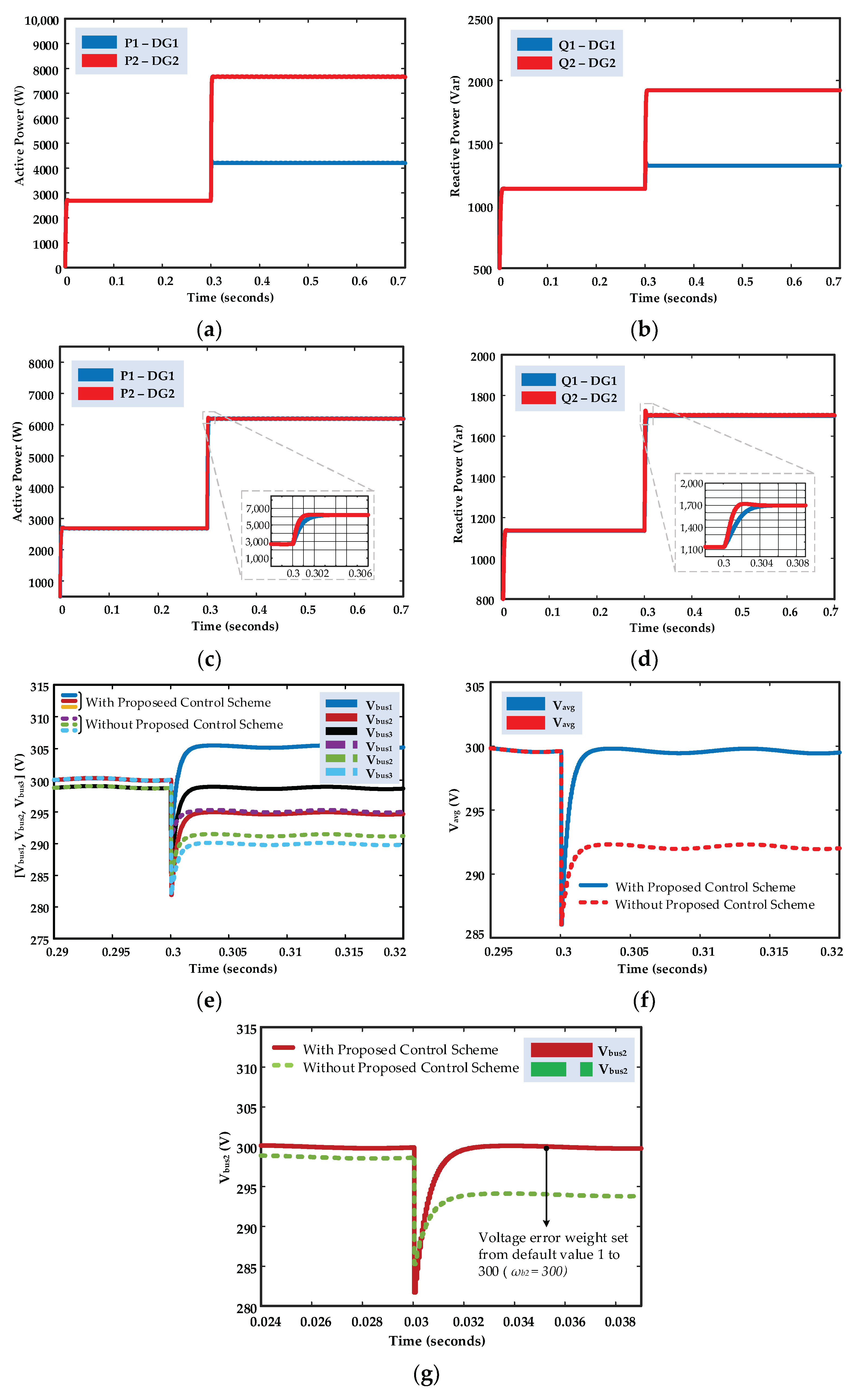
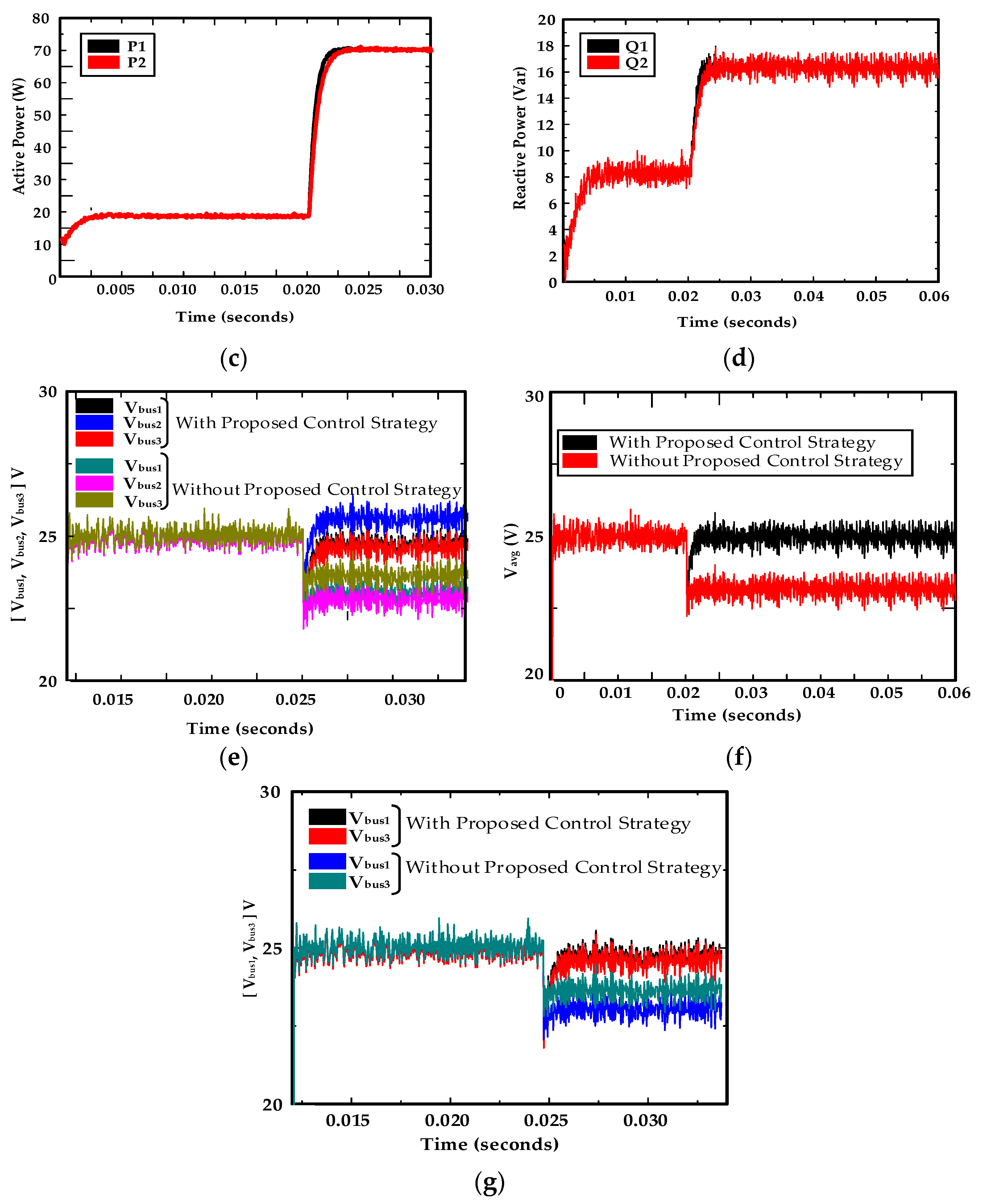
5.2.1. Case 1: Power Sharing and Bus 2 Voltage Control

The primary objective of this case study is to observe the power-sharing and load bus 2 voltage performance. The voltage magnitude of bus 2 should be at its original state, i.e., Vref = 300 V, in the presence of load disturbance. Initially, the voltage error weights wb1, wb2, and wb3 for three buses are set at a default value of 1. A disturbance load Ld2/Rd2 with values of Ld2 = 69 mH and Rd2 = 9.9 ohms is now added at bus 2 at 0.3 s. The behavior of voltage regulation, active, and reactive power sharing under disturbance load is shown in Figure 9. An obvious active, reactive power sharing error is observed once the Ld2/Rd2 is added as illustrated in Figure 9a,b, which is later compensated to almost zero once the proposed control scheme is activated at 0.3 s as depicted in Figure 9c,d. All three load buses voltage curve behavior is shown in Figure 9f. A rough average of 7 V voltage deviations are observed in Figure 9g which is compensated to almost zero once the proposed strategy is activated. The 6 V voltage deviation occurs at bus 2 and even the proposed control scheme is activated, shown in Figure 9e by the red cure. This deviation is removed and bus 2 voltage is regulated by varying the respective voltage error weight wb2, set from 1 to 300, as depicted in Figure 9g.

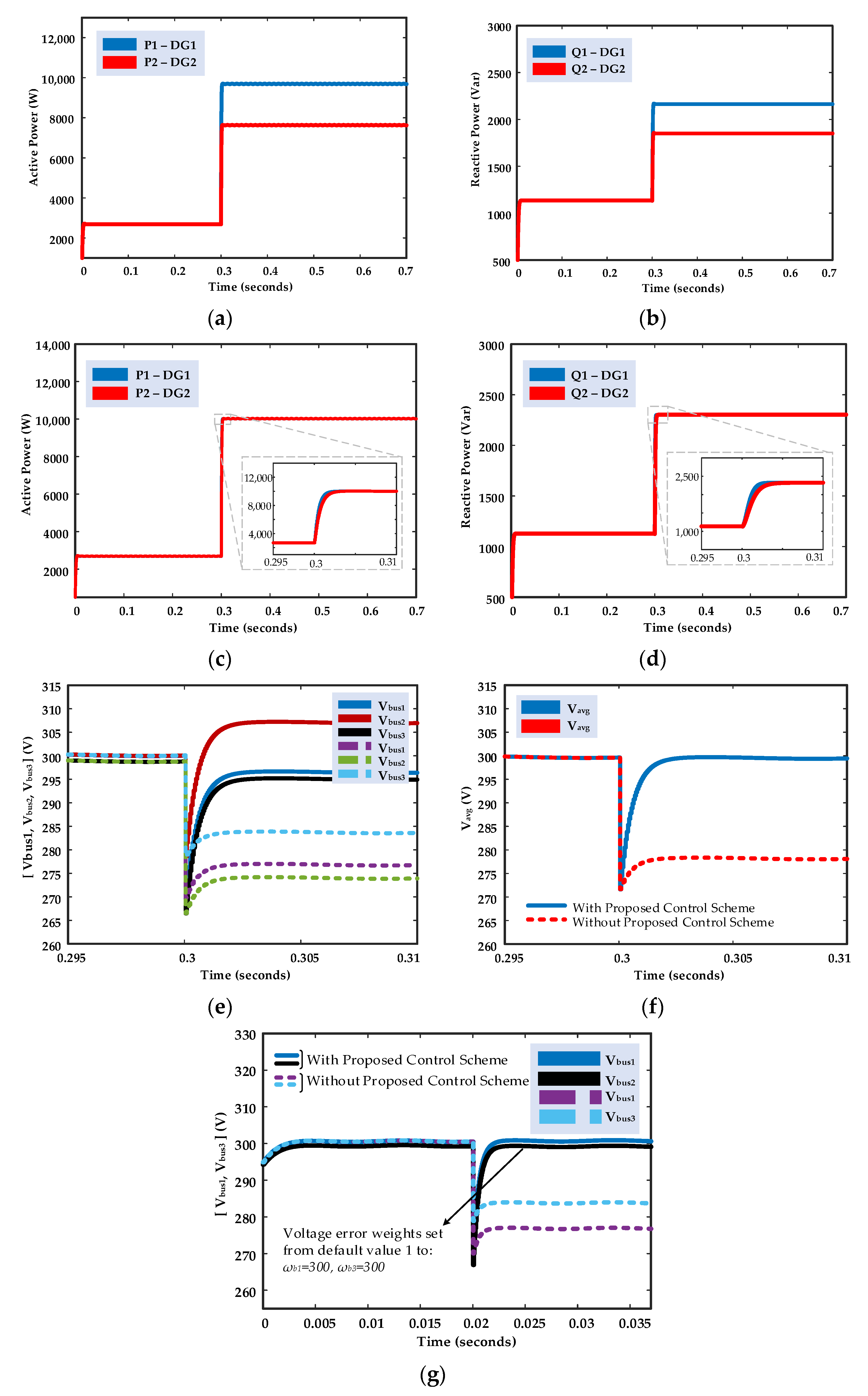
5.2.2. Load Variation at Bus 1 and Bus 2 Simultaneously

To further investigate the superior control performance of the proposed optimal control strategy two disturbance loads (Ld1 = 69 mH, Rd1 = 9.9 ohm, Ld3 = 69 mH and Rd3 = 9.9 ohm) are exerted at bus 1 and bus 3, simultaneously. It is observed that the disturbance leads to a heavy power-sharing error and respective bus voltage drop, shown in Figure 10. Active and reactive power response with conventional control scheme is demonstrated by Figure 10a,b. Such power-sharing errors are eliminated and compensated to almost zero, once the proposed methodology is activated at time 0.3 s, illustrated in Figure 10c,d. Three load buses voltage response and average voltage response with and without presented control schemes are depicted in Figure 10e,f, respectively. Figure 10e shows the average of 5 V volts deviation at bus1 and bus 3, and even the control strategy was activated. This deviation is improved and restored to a nominal voltage by varying both buses voltage error weights, set from default value 1 to 300 (ωb1 = 300 and ωb3 = 300) as demonstrated in Figure 10g.
Distributed secondary control strategy is used to regulate the system frequency. In Figure 11, it is noticed that activation of the proposed strategy at time 0.02 s, yields frequency restoration within an acceptable range of ±0.5 Hz.

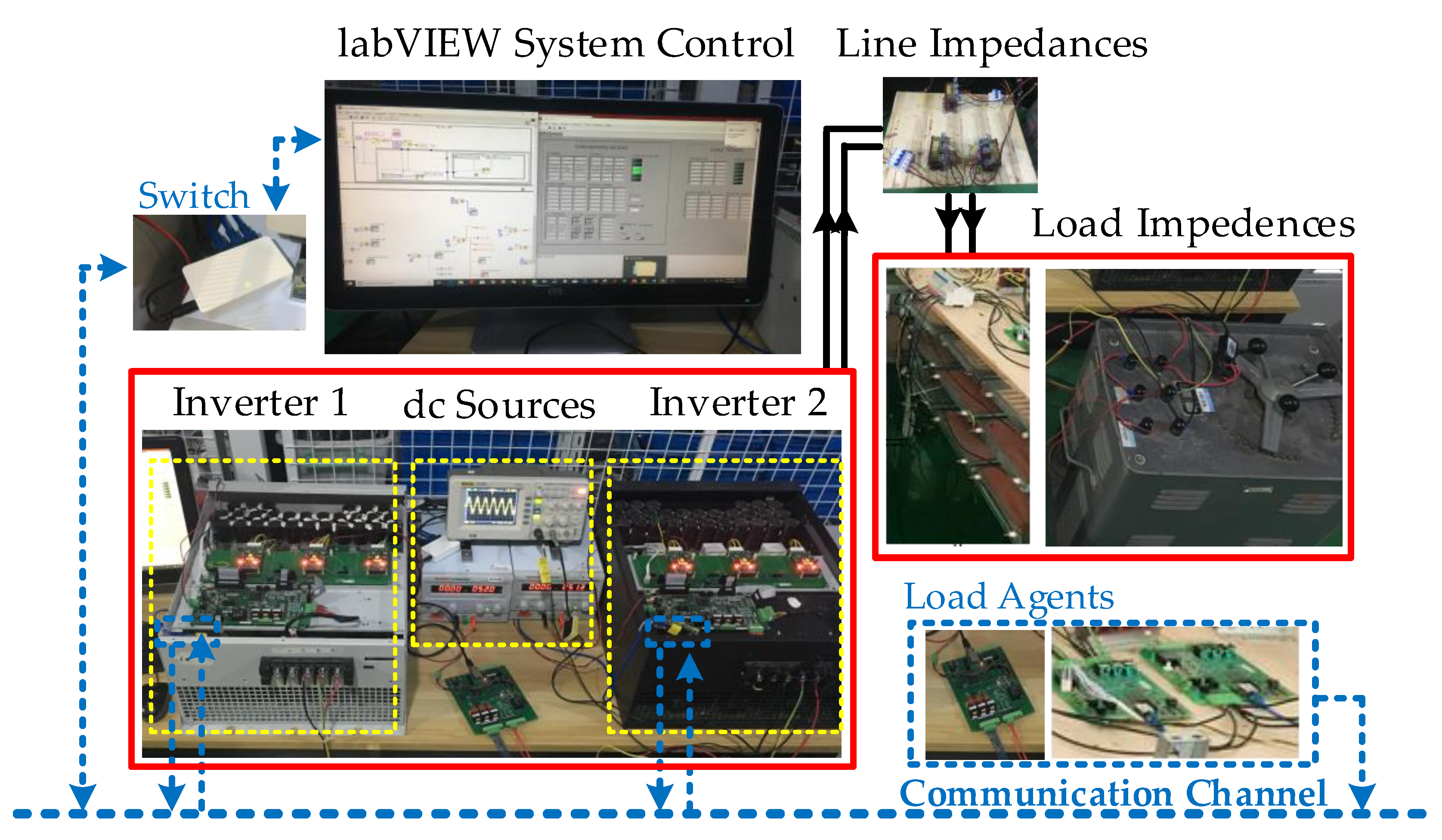
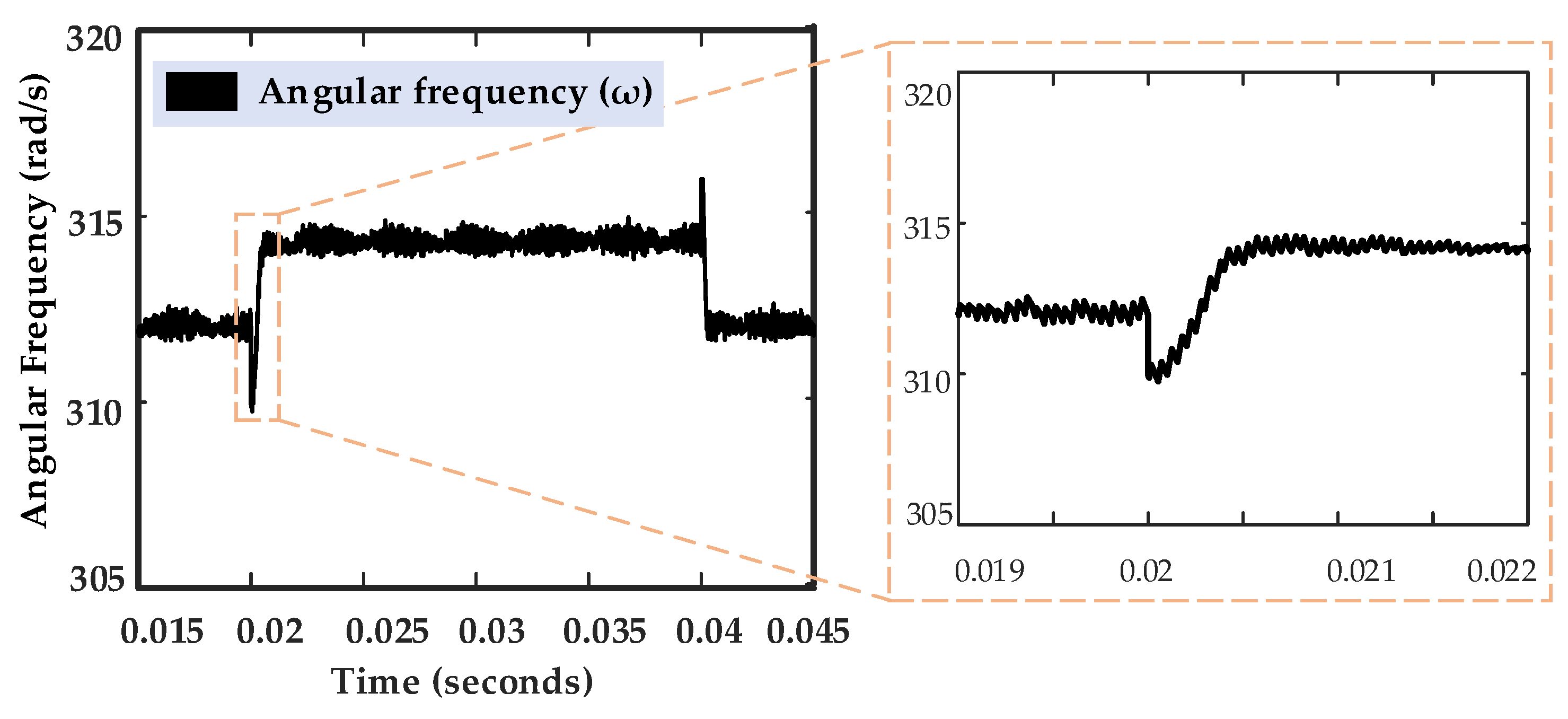
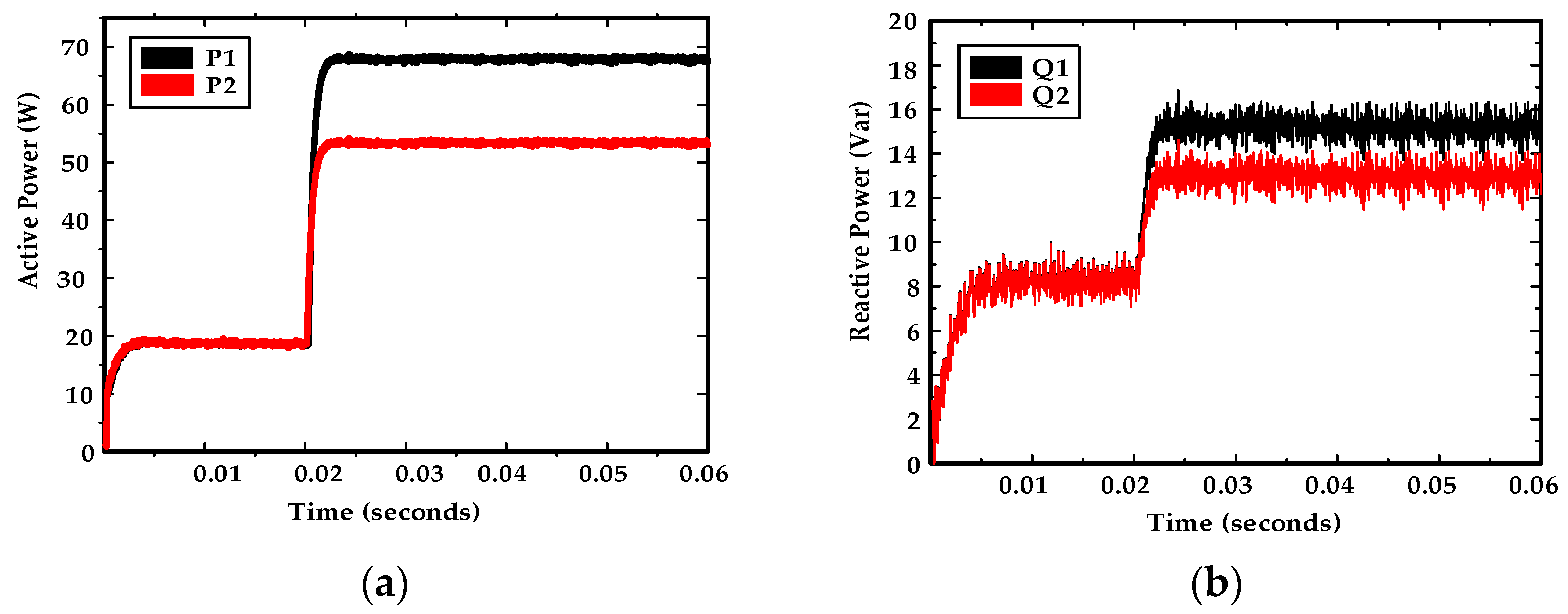
5.3. Experimental Results

An accompanying experiment is conducted to validate simulation results, wherein the disturbance load Ld2/Rd2 is exerted at bus 2 at time 0.02 s. Power-sharing error and voltage deviations caused by disturbance are depicted in Figure 12. Real and reactive power sharing curve response with conventional scheme is demonstrated by Figure 12a,b, respectively. From Figure 12c,d, the real and reactive power sharing errors are compensated almost to zero once the proposed optimal control methodology is activated. All three load buses voltage response curve are collectively shown by Figure 12e, where the initial conditions of parameters are same for both conventional and proposed control strategies. Figure 12f illustrates the average buses voltage response, where it is observed the average bus voltage deviation is restored to its original value (black cure) once the proposed control strategy is activated. Figure 13 shows the variation of optimal control commands uc1 (28.25 − 0.3j V) and uc2 (27.30 V), before and after the disturbance load exertion. Good agreement is observed by comparing the simulation and experimental results. The effectiveness of the proposed optimal control scheme is thus confirmed.

6. Conclusions

In this paper, an optimal control technique is presented for islanded MG. This study performs two tasks: load estimation and an optimal regulator. The load estimation strategy approximated the grid impedance and transmitted the information through a communication channel. An equality constraints optimized problem, called an optimal regulator, sends optimal control commands to respective inner voltage control layers of each DG unit. In parallel, a secondary layer is implemented to regulate system frequency. To observe the effectiveness of the proposed methodology, we have exerted the disturbance loads at bus 2 as well as bus 1 and 2, simultaneously. In accordance with the proposed optimized cost function, the MG is at the optimum operating point as verified through the case simulation and hardware studies. Modeling and analysis of three-phase inverter-based MG was also verified through stability analysis using system-wide mathematical small-signal models.

Author Contributions

Conceptualization, M.Z.K., C.M. and S.H.; methodology, M.Z.K. and S.H.; software, M.Z.K., K.H. and W.A.; validation, M.Z.K., S.H. and K.H.; formal analysis, E.M.A., S.H. and W.A.; investigation, C.M.; resources, W.A. and E.M.A.; writing—original draft preparation, M.Z.K.; writing—review and editing, E.M.A. and S.H.; visualization, K.H. and E.M.A.; supervision, C.M.; project administration, W.A. and E.M.A.; funding acquisition, W.A. and E.M.A. All authors have read and agreed to the published version of the manuscript.

Funding

The authors extend their appreciation to the Deputyship for Research & Innovation, Ministry of Education in Saudi Arabia for funding this work through the project number “375213500”. The authors also would like to extend their sincere appreciation to the central laboratory at Jouf University for support this study.

Institutional Review Board Statement

Not applicable.

Informed Consent Statement

Not applicable.

Acknowledgments

The authors would like to thank the editor in chief, the associate editors, and the reviewers for their worthy suggestions, time, and effort in improving and finalizing this paper. The authors would further like to thank Sajid A. Khan ([email protected]) for providing the support and resources.

Conflicts of Interest

The authors declare no conflict of interest.

Appendix A

u d = 2 3 ( u a sin ( ϑ i ) + u b sin ( ϑ i 2 π / 3 ) + u c sin ( ϑ i + 2 π / 3 ) ) u q = 2 3 ( u a cos ( ϑ i ) + u b cos ( ϑ i 2 π / 3 ) + u c cos ( ϑ i + 2 π / 3 ) ) u 0 = 1 3 ( u a + u b + u c )
where the uabc are the bus voltage or current three-phase signal to dq0 rotating reference frame.
Transformation Matrices
K p t v = K p t i = [ sin ( ϑ i ) cos ( ϑ i ) 0 cos ( ϑ i ) sin ( ϑ i ) 0 0 0 1 ]  

Appendix B. Transformation Matrices

S i = V i j = 1 N Y i j * V j * = | V i | φ i j = 1 N ( G i j + j B i j ) * ( | V j | φ j ) = | V i | φ i j = 1 N ( G i j j B i j ) ( | V j | φ j )
= j = 1 N   | V i | φ i ( | V j | φ j ) ( G i j j B i j ) = j = 1 N   | V i | | V j | ( φ i φ j ) ( G i j j B i j )
By converting the phasor expression into a complex function of sinusoids, i.e., V = |V|∠φ = |V|(cosφ + jsinφ),
S i = j = 1 N   | V i | | V j | ( φ i φ j ) ( G i j j B i j )
= j = 1 N   | V i | | V j | ( cos ( φ i φ j ) + j sin ( φ i φ j ) ) ( G i j j B i j )
= P i + j Q i

Appendix C. Grid Side Filter Model

The small-signal model of LC output filter and coupling inductance by assuming that voltage provided by the inverter is the same as the demand voltage is expressed as:
d i l d q i d t = R f i L f i . i l d q i ± ω i . i l q q i + 1 L f i . v i d q i 1 L f i . v o d q i
d v o d q i d t = ω i . v o d q i + 1 C f i . i l d q i 1 C f i . I o d q i
d i o d q i d t = R c i L c i . i o d q i + ω i . i o d q i + 1 L c i . v o d q i 1 L c i . v o b d q i
LC filter and coupling inductance, there linearization small signal equations re represented in following equation, where wo,
[ Δ i . l d q i Δ v o d q i Δ i o d q i ] = A G S F [ Δ i l d q i Δ v o d q i Δ i o d q i ] + B G S F 1 [ Δ v i d q i ] + B G S F 2 [ Δ v b d q i ] + B G S F 3 [ Δ ω ]

Appendix D. Complete Model of an ith Inverter

The output currents are the output variables of ith inverters which can be expressed in vector form ∆iodqi. ∆ioDQi, which is a small-signal output current, expressed as:
[ Δ i o D Q ] = [ T γ ] . [ Δ i o d q ] + [ T ζ ] . [ Δ δ ] = [ cos ( δ ) sin ( δ ) sin ( δ ) cos ( δ ) ] . [ Δ i o d q ] + [ I o d cos ( δ ) I o q sin ( δ ) I o d sin ( δ ) I o q cos ( δ ) ] . [ Δ δ ]
T γ = [ cos ( δ ) sin ( δ ) sin ( δ ) cos ( δ ) ] . [ Δ i o d q ]   ;   T ζ = [ I o d cos ( δ ) I o q sin ( δ ) I o d sin ( δ ) I o q cos ( δ ) ] . [ Δ δ ]
Bus voltage on the common reference frame is the input signal to the ith inverter model. Therefore, by using reverse transformation, the bus voltage can be converted into an ith individual inverter reference frame.
[ Δ u b d q ] = [ T γ 1 ] . [ Δ u b D Q ] + [ T σ 1 ] [ Δ δ ] ,   where ,   T σ 1 = [ U b D sin ( δ ) + U b Q cos ( δ ) U b D cos ( δ ) U b Q sin ( δ ) ]
By combining the aforementioned state-space models for three controllers of an ith inverter the complete small-signal model can be obtained.
[ Δ x ˙ i n v i ] = A i n v i . [ Δ x i n v i ] + B i n v i . [ Δ u b D Q i ] + B i ω c o m . [ Δ ω c o m ]
[ Δ ω i Δ i o D Q ] = [ C i n v ω i C i n v c i ] . [ Δ x i n v i ]
where,
[ Δ x i n v ] = [ Δ δ i Δ P i Δ Q i Δ φ d i Δ φ q i Δ γ d i Δ γ q i Δ i l d i Δ i l q i Δ v o d i Δ v o q i Δ i o d i Δ i o q i ] T
A i n v i = [ A P i 0 0 B P i B v 1 i C P v i 0 0 B v 2 i B G S F i D v 1 i C P v i B c 1 i C v i 0 B c 1 i D v 2 i + B c 2 i B G S F 2 i   [ T v i 1   0   0 ] + B G S F 3 i C p w i B G S F 1 i D c 1 i C v i B G S F 1 i C c i A G S F i + B G S F 1 i ( D c 1 i D v 2 i + D c 2 i ) ] 13 × 13
B i n v i = [ 0 0 0 B G S F 2 T S 1 ] 13 × 2 B i w c o m = [ B p w c o m 0 0 0 ] 13 × 1 ;   C i n v w i = ( [ C p w   0   0   0 ] 1 × 13 i = 1 [ 0   0   0   0 ] 1 × 13 i 1 )
C i n v c i = [ [ T C   0   0 ]   0   0   [ 0   0   T s ] ] 2 × 13

Appendix E. Combined Model of N Inverters

In MG, the N number of DG inverters may be operating as a source at variable distances among each other. In this section, our approach is to discuss the possible sub-models form of all individual ith to kth DG inverters and combine them to the existing corresponding network. The combined small-signal model of “N” number of DG inverters can be represented as:
[ Δ x . i n v ] = A i n v . [ Δ x i n v ] + B i n v . [ Δ v b D Q ]
[ Δ i o D Q ] = C i n v c . [ Δ x i n v ]
where,
[ Δ x i n v ] = A i n v . [ Δ x i n v 1 Δ x i n v 2 Δ x i n v N ] T ;   A i n v = [ A i n v 1 + B 1 w c o m C i n v w 1 0 0 A i n v 2 + B 2 w c o m C i n v w 1 ] 13 N × 13 s
B i n v = [ B i n v 1 B i n v 2 ] 13 N × 2 m ;   [ Δ v b D Q ] = [ Δ v b D Q 1 Δ v b D Q 2 Δ v b D Q N ] ;   C i n v c = [ [ C i n v c 1 ] 0 0 [ C i n v c 2 ] ] 2 N × 13 N

Appendix F. Network and Load Model

If an ith feeder line is connected between node j and k, then algebraic equations can be presented as the following:
d i lineDi d t = R l i n e i L l i n e i i l i n e D i + ω i l i n e Q i + 1 L l i n e i v b D j 1 L l i n e i v b D k
d i lineQi d t = R l i n e i L l i n e i i l i n e Q i ω i l i n e D i + 1 L l i n e i v b Q j 1 L l i n e i v b Q k
[ Δ i . l i n e D Q ] = A L I N E . [ Δ i l i n e D Q ] + B 1 L I N E . [ Δ u b D Q i ] + B 2 L I N E . Δ ω
where,
[ Δ i . l i n e D Q ] = [ Δ i l i n e D Q 1   Δ i l i n e D Q 2 Δ i l i n e D Q n ] T ,   [ Δ u b D Q i ] = [ Δ i b D Q 1   Δ i b D Q 2 Δ i b D Q m ] T ,   Δ ω = Δ ω c o m
A L I N E = [ A L I N E 1 0 0 A L I N E 2 ] 2 n × 2 n ;   B 1 L I N E = [ B 1 L I N E 1 B 1 L I N E 2 ] 2 n × 2 m B 2 L I N E = [ B 2 L I N E 1 B 2 L I N E 2 ] 2 n × 1 ;  
A L I N E i = [ R l i n e i L l i n e i ω i ω i R l i n e i L l i n e i ] B 2 L I N E i = [ I l i n e Q i I l i n e D i ]   B 1 L I N E i = [ 0 1 L l i n e i 0 0 ] 2 × 2 m
The state equations for RL load connected via an ith node can be written as follows:
d i loadDi d t = R l o a d i L l o a d i i l o a d i D i + ω i l o a d i Q i + 1 L l o a d i v b D i
d i loadQi d t = R l o a d i L l o a d i i l o a d i Q i ω i l o a d i D i + 1 L l o a d i v b Q i
Therefore, if there are p load points available in a particular network then the small-signal model can be presented as:
[ Δ i . l o a d D Q ] = A L O A D . [ Δ i l o a d D Q ] + B 1 L L O A D . [ Δ u b D Q i ] + B 2 L O A D . Δ ω i
A L O A D = [ A L O A D 1 0 0 A L O A D 2 ] 2 p × 2 p ,   B 1 L O A D = [ B 1 L O A D 1 B 1 L O A D 2 ] 2 P × 2 m ,   B 2 L O A D = [ B 2 L O A D 1 B 2 L O A D 2 ] 2 n × 1
where,
A L O A D i = [ R l o a d i L l o a d i ω i ω i R l o a d i L l o a d i ] ,   B 2 LOAD = [ I l o a d Q i I l o a d Q i ] ,   B 1 L O A D i = [ 0 1 L l o a d i 0 0 ] 2 × 2 m

References

  1. Khan, M.Z.; Mu, C.; Habib, S.; Alhosaini, W.; Ahmed, E.M. An Enhanced Distributed Voltage Regulation Scheme for Radial Feeder in Islanded Microgrid. Energies 2021, 14, 6092. [Google Scholar] [CrossRef]
  2. Ali, S.; Kazmi, A.; Shahzad, M.K.; Khan, A.Z.; Shin, D.R. Smart Distribution Networks: A Review of Modern Distribution Concepts from a Planning Perspective. Energies 2017, 10, 501. [Google Scholar]
  3. Habib, S.; Khan, M.M.; Abbas, F.; Ali, A.; Hashmi, K.; Shahid, M.U.; Bo, Q.; Tang, H. Risk Evaluation of Distribution Networks Considering Residential Load Forecasting with Stochastic Modeling of Electric Vehicles. Energy Technol. 2019, 7, 1900191. [Google Scholar] [CrossRef]
  4. Abdalla, O.H.; Fayek, H.H.; Ghany, A.; Ghany, M.A. Secondary and Tertiary Voltage Control of a Multi-Region Power System. Electricity 2020, 1, 37–59. [Google Scholar] [CrossRef]
  5. Baran Junior, A.R.; Piazza Fernandes, T.S.; Borba, R.A. Voltage Regulation Planning for Distribution Networks Using Multi-Scenario Three-Phase Optimal Power Flow. Energies 2020, 13, 159. [Google Scholar] [CrossRef] [Green Version]
  6. Khan, M.Z.; Khan, M.M.; Jiang, H.; Hashmi, K.; Shahid, M.U. An improved control strategy for three-phase power inverters in islanded ac microgrids. Inventions 2018, 3, 47. [Google Scholar] [CrossRef] [Green Version]
  7. Eid, B.M.; Rahim, N.A.; Selvaraj, J.; El Khateb, A.H. Control Methods and Objectives for Electronically Coupled Distributed Energy Resources in Microgrids: A Review. IEEE Syst. J. 2016, 10, 446–458. [Google Scholar] [CrossRef]
  8. Hashmi, K.; Khan, M.M.; Shahid, M.U.; Nawaz, A.; Khan, A.; Jun, J.; Tang, H. An energy sharing scheme based on distributed average value estimations for islanded AC microgrids. Int. J. Electr. Power Energy Syst. 2020, 116, 105587. [Google Scholar] [CrossRef]
  9. Hashmi, K.; Khan, M.M.; Xu, J.; Shahid, M.U.; Habib, S.; Faiz, M.T.; Tang, H. A Quasi-average estimation aided hierarchical control scheme for power electronics-based islanded microgrids. Electronics 2019, 8, 39. [Google Scholar] [CrossRef] [Green Version]
  10. Habib, S.; Khan, M.M.; Abbas, F.; Numan, M.; Ali, Y.; Tang, H.; Yan, X. A framework for stochastic estimation of electric vehicle charging behavior for risk assessment of distribution networks. Front. Energy 2019, 14, 298–317. [Google Scholar] [CrossRef]
  11. Shahid, M.U.; Khan, M.M.; Yuning, J.; Hashmi, K.; Mumtaz, M.A.; Khan, M.Z. An adaptive droop technique for load sharing in islanded DC micro grid with faulty communication. EPE J. 2021, 1–15. [Google Scholar] [CrossRef]
  12. Tuladhar, A.; Jin, H.; Unger, T.; Mauch, K. Control of Parallel Inverters in Distributed AC Power Systems with Consideration of Line Impedance Effect. IEEE Trans. Ind. Appl. 2000, 36, 131–138. [Google Scholar] [CrossRef]
  13. Pei, Y.; Jiang, G.; Yang, X.; Wang, Z. Auto-Master-Slave Control Technique of Par allel Inverters in Distributed AC Power Systems and UPS. In Proceedings of the 2004 IEEE 35th Annual Power Electronics Specialists Conference (IEEE Cat. No.04CH37551), Aachen, Germany, 20–25 June 2004; pp. 2050–2053. [Google Scholar]
  14. Microgrids, V. Decentralized Cooperative Control Strategy of Microsources for Stabilizing Autonomous VSC-based microgrids. IEEE Trans. Power Syst. 2012, 27, 1949–1959. [Google Scholar]
  15. Vandoorn, T.L.; de Kooning, J.D.M.; Meersman, B.; Vandevelde, L. Review of primary control strategies for islanded microgrids with power-electronic interfaces. Renew. Sustain. Energy Rev. 2013, 19, 613–628. [Google Scholar] [CrossRef]
  16. Sun, X.; Lee, Y.; Xu, D. Modeling, Analysis, and Implementation of Parallel Multi-Inverter Systems with Instantaneous average-current-sharing scheme. IEEE Trans. Power Electron. 2003, 18, 844–856. [Google Scholar]
  17. Guerrero, J.M.; Matas, J.; de Vicuña, L.G.; Castilla, M.; Miret, J. Decentralized Control for Parallel Operation of Distributed Generation Inverters Using Resistive Output Impedance. IEEE Trans. Ind. Electron. 2007, 54, 994–1004. [Google Scholar] [CrossRef]
  18. Yao, W.; Chen, M.; Matas, J.; Guerrero, J.M.; Qian, Z.M. Design and analysis of the droop control method for parallel inverters considering the impact of the complex impedance on the power sharing. IEEE Trans. Ind. Electron. 2011, 58, 576–588. [Google Scholar] [CrossRef]
  19. Guerrero, J.M.; Vasquez, J.C.; Matas, J.; de Vicuña, L.G.; Castilla, M. Hierarchical control of droop-controlled AC and DC microgrids—A general approach toward standardization. IEEE Trans. Ind. Electron. 2011, 58, 158–172. [Google Scholar] [CrossRef]
  20. He, J.; Li, Y.W.; Guerrero, J.M.; Blaabjerg, F.; Vasquez, J.C. An Islanding Microgrid Power Sharing Approach Using Enhanced Virtual Impedance Control Scheme. IEEE Trans. Power Electron. 2013, 28, 5272–5282. [Google Scholar] [CrossRef]
  21. Li, Y.; Li, Y.W. Decoupled Power Control for an Inverter Based Low Voltage Microgrid in Autonomous Operation. In Proceedings of the 2009 IEEE 6th International Power Electronics and Motion Control Conference, Wuhan, China, 17–20 May 2009; Volume 3, pp. 2490–2496. [Google Scholar]
  22. Habib, S.; Khan, M.M.; Abbas, F.; Ali, A.; Faiz, M.T.; Ehsan, F.; Tang, H. Contemporary Trends in Power Electronics Converters for Charging Solutions of Electric Vehicles. CSEE J. Power Energy Syst. 2020, 6, 911–929. [Google Scholar] [CrossRef]
  23. Li, Y.; Li, Y.W. Power management of inverter interfaced autonomous microgrid based on virtual frequency-voltage frame. IEEE Trans. Smart Grid 2011, 2, 30–40. [Google Scholar] [CrossRef]
  24. Perreault, D.J.; Selders, R.L.; Kassakian, J.G. Frequency-Based Current-Sharing Techniques for Paralleled Power Converters. IEEE Trans. Power Electron. 1998, 13, 626–634. [Google Scholar] [CrossRef]
  25. He, J.; Li, Y.W. An Enhanced Microgrid Load Demand Sharing Strategy. IEEE Trans. Power Electron. 2012, 27, 3984–3995. [Google Scholar] [CrossRef]
  26. Vasquez, J.C.; Guerrero, J.; Luna, A.; Rodriguez, P.; Teodorescu, R. Adaptive Droop Control Applied to Voltage-Source Inverters Operating in Grid-Connected and Islanded Modes. IEEE Trans. Ind. Electron. 2009, 56, 4088–4096. [Google Scholar] [CrossRef]
  27. He, J.; Li, Y.W. An accurate reactive power sharing control strategy for DG units in a microgrid. In Proceedings of the 8th International Conference on Power Electronics—ECCE Asia, Jeju, Korea, 30 May–3 June 2011; pp. 551–556. [Google Scholar] [CrossRef]
  28. Majumder, R.; Ghosh, A.; Ledwich, G.; Zare, F. Angle Droop versus Frequency Droop in a Voltage Source Converter Based Autonomous Microgrid. In Proceedings of the 2009 IEEE Power & Energy Society General Meeting, Calgary, AB, Canada, 26–30 July 2009. [Google Scholar]
  29. Majumder, R.; Chaudhuri, B.; Ghosh, A.; Majumder, R.; Ledwich, G.; Zare, F. Improvement of Stability and Load Sharing in an Autonomous Microgrid Using Supplementary Droop Control Loop. IEEE Trans. Power Syst. 2010, 25, 796–808. [Google Scholar] [CrossRef] [Green Version]
  30. Han, H.; Hou, X.; Yang, J.; Wu, J.; Su, M.; Guerrero, J.M. Review of power sharing control strategies for islanding operation of AC microgrids. IEEE Trans. Smart Grid 2016, 7, 200–215. [Google Scholar] [CrossRef] [Green Version]
  31. Han, Y.; Li, H.; Shen, P.; Coelho, E.A.A.; Guerrero, J.M. Review of Active and Reactive Power Sharing Strategies in Hierarchical Controlled Microgrids. IEEE Trans. Power Electron. 2017, 32, 2427–2451. [Google Scholar] [CrossRef] [Green Version]
  32. Raj, D.C.; Gaonkar, D.N. Frequency and Voltage Droop Control of Parallel Inverters in Microgrid. In Proceedings of the 2016 2nd International Conference on Control, Instrumentation, Energy & Communication (CIEC), Kolkata, India, 28–30 January 2016; Volume 2, pp. 407–411. [Google Scholar]
  33. Zhong, Q. Robust Droop Controller for Accurate Proportional Load Sharing Among Inverters Operated in Parallel. IEEE Trans. Ind. Electron. 2013, 60, 1281–1290. [Google Scholar] [CrossRef]
  34. Khan, M.Z.; Khan, M.M.; Xiangming, X.; Khalid, U.; Rasool, M.A.U. An optimal control load demand sharing strategy for multi-feeders in islanded microgrid. Int. J. Adv. Comput. Sci. Appl. 2018, 9, 18–25. [Google Scholar] [CrossRef]
  35. Rocabert, J.; Luna, A.; Blaabjerg, F.; Rodríguez, P. Control of power converters in AC microgrids. IEEE Trans. Power Electron. 2012, 27, 4734–4749. [Google Scholar] [CrossRef]
  36. Lee, C.T.; Chu, C.C.; Cheng, P.T. A new droop control method for the autonomous operation of distributed energy resource interface converters. IEEE Trans. Power Electron. 2013, 28, 1980–1993. [Google Scholar] [CrossRef]
  37. Matas, J.; Castilla, M.; De Vicuña, L.G.; Miret, J.; Vasquez, J.C. Virtual impedance loop for droop-controlled single-phase parallel inverters using a second-order general-integrator scheme. IEEE Trans. Power Electron. 2010, 25, 2993–3002. [Google Scholar] [CrossRef]
  38. Wang, X.; Li, Y.W.; Blaabjerg, F. Virtual-Impedance-Based Control for Voltage-Source and Current-Source Converters. IEEE Trans. Power Electron. 2015, 30, 7019–7037. [Google Scholar] [CrossRef]
  39. Guerrero, J.M.; de Vicuña, L.G.; Matas, J.; Miret, J.; Castilla, M. Output impedance design of parallel-connected UPS inverters. IEEE Int. Symp. Ind. Electron. 2004, 2, 1123–1128. [Google Scholar] [CrossRef]
  40. Zmood, D.N.; Holmes, D.G. Stationary frame current regulation of PWM inverters with zero steady-state error. IEEE Trans. Power Electron. 2003, 18, 814–822. [Google Scholar] [CrossRef]
  41. Wang, Y.; Chen, Z.; Wang, X.; Tian, Y.; Tan, Y. An Estimator-Based Distributed Voltage-Predictive Control Strategy for AC Islanded Microgrids. IEEE Trans. Power Electron. 2015, 30, 3934–3951. [Google Scholar] [CrossRef]
  42. Wang, Y.; Wang, X.; Chen, Z.; Blaabjerg, F. Distributed Optimal Control of Reactive Power and Voltage in Islanded Microgrids. IEEE Trans. Ind. Appl. 2017, 53, 340–349. [Google Scholar] [CrossRef]
Figure 1. Design procedures of the proposed control strategy.
Energies 14 06490 g001
Figure 2. MG power network model and proposed control strategy.
Energies 14 06490 g002
Figure 3. Proposed load estimation scheme. (a) Each load-bus impedance is estimated through local load node agents. (b) Representation of approximated grid impedance in term of 1 load-bus configuration.
Energies 14 06490 g003
Figure 4. (a) MG optimal regulator’s algorithm flowchart; (b) and (c) shows surface plots (3D) of minima (i.e., fvalue) and optimal control commands (uc1, uc2) at different disturbance load.
Energies 14 06490 g004
Figure 5. (a) Power controller of ith inverter. (b) Inner control loops: voltage and current controller.
Energies 14 06490 g005
Figure 6. Live laboratory experimental prototype.
Energies 14 06490 g006
Figure 7. Effect of mP variation.
Energies 14 06490 g007
Figure 8. Effect of the time delay td on system stability.
Energies 14 06490 g008
Figure 9. Simulation results. (a) Active power response without proposed control scheme. (b) Reactive power response without proposed control scheme. (c) Proportional active power sharing proposed control strategy. (d) Proportional reactive power sharing with proposed control strategy. (e) Load buses Vbus1, Vbus2 and Vbus3 response curve. (f) Average load bus voltage curve of Vbus1, Vbus2 and Vbus3. (g) Load bus Vbus2 response by changing ωb2 from 1 to 300.
Energies 14 06490 g009
Figure 10. Simulation results. (a) Active power response without proposed control scheme. (b) Reactive power response without proposed control scheme. (c) Proportional active power sharing proposed control scheme. (d) Proportional reactive power sharing with proposed control scheme. (e) Load buses Vbus1, Vbus2 and Vbus3 response curve. (f) Average load bus voltage curve of Vbus1, Vbus2 and Vbus3 (g) Vbus1 and Vbus3 voltage curve by weight (ωb1, ωb2) variation from 1 to 300.
Energies 14 06490 g010
Figure 11. System frequency regulation curve.
Energies 14 06490 g011
Figure 12. Experiments results. (a) Active power response without proposed control scheme. (b) Reactive power response without proposed control scheme. (c) Proportional active power sharing proposed control scheme. (d) Proportional reactive power sharing with proposed control scheme. (e) Three buses Vbus1, Vbus2 and Vbus3 response. (f) Average voltage response of Vbus1, Vbus2 and Vbus3 (g) Vbus1 and Vbus3 voltage response.
Energies 14 06490 g012aEnergies 14 06490 g012b
Figure 13. An optimal control inputs (uci) to lab-scaled distributed generation units (a) Variation of uci (uc1, uc2) under disturbance load at 0.02 s. (b) An imaginary part (v1q) of uc1 curve, in red, on smith chart.
Energies 14 06490 g013
Table 1. System parameters for simulation and experiment.
Sr.ComponentsUnitsComponentsUnits
1Nominal frequency50 HzLload1/Rload180 mH/60 Ω
2Simulations Vref
Experiments Vref
300 V
25 V
Lload2/Rload2
Lload3/Rload3
80.5 mH/61 Ω
120 mH/80 Ω
3Switching Frequency16 KHz--
4Lc1/Lc2
Lline1/Rline1
Lline2/Rline2
1 mH/1 mH
0.5 mH/0.75 Ω
0.5 mH/0.75 Ω
Ld1/Rd1
Ld2/Rd2
Ld3/Rd3
10.5 mH/19 Ω
9.5 mH/20.5 Ω
10 mH/21 Ω
5mP1/mP21.5 × 10−4/0.5 × 10−2ωb1, ωb2, ωb3300, 500, 300
Table 2. System parameters for stability analysis and experimental prototype.
Sr. No.Control Parameters for Stability Analysis
1Droop gainsMinMax
mP0.020.32
2Frequency restoration
kpf0.452.9
kif0.20.9
3Voltage restoration
kpV0.32.5
kiV0.080.48
4Time delay
τdelay06
Sr. No.Control Parameters for Experimental Prototype
ComponentsUnitsComponentsUnits
1.Operating frequency50 HzSampling rate1 ms
2.DG units’ ratings3 A, 30 VjXi1, jXi2200 uH
3.jXc1, jXc220 uFjXg1, jXg260 uH
Publisher’s Note: MDPI stays neutral with regard to jurisdictional claims in published maps and institutional affiliations.

