1. Introduction
MEMS-based acceleration sensors are widely used in many applications [
1,
2,
3,
4,
5]. Generally, we can distinguish the following sensors: one-axis and three-axis accelerometers according to their design [
6,
7]. Three-axis accelerometers can be manufactured as a sensor with one seismic mass or with three one-axis independent structures (for X, Y and Z axis separately).
In particular, capacitive accelerometers have proved to be especially popular [
8], due to their high sensitivity, low manufacturing cost, small size, and stability. Monolithic capacitive MEMS accelerometers are, for example, reported in [
9]. The construction of the in-plane accelerometers is well-known: most often, comb-drive structure is used to measure the acceleration, which is proportional to the capacitance change [
10]. Although capacitive MEMS accelerometers have fairly low temperature sensitivity, their performance, especially in high temperature range applications, can be seriously degraded by the temperature drift [
11,
12]. Thermal expansion in a wide temperature range results in the change of suspension stiffness and readout part dimensions. Therefore, both the bias and the scale factor of the accelerometer are affected by temperature and introduce errors in the sensor’s response.
One of the other problematic issues in differential capacitive sensors is the presence of the post-manufacturing mismatch. The residual stress induced to the structure during the fabrication process can result in two sensor capacitors having different values, potentially shifting the output level outside the range of the readout circuit. This mismatch can be quite easily compensated for using various methods [
13,
14]. However, in what follows, we will show that, although it is possible to nullify the impact of the mismatch itself by using a dedicated compensation circuit, this mismatch, even if compensated, will inadvertently increase the temperature drift and, in turn, degrade the sensor’s performance.
Thermal issues in MEMS capacitive sensors have been heavily investigated by scientists. In [
15], the authors analyzed the temperature drift of bias (TDB) and the temperature drift of scale factor (TDSF). They compared symmetric and asymmetric structures of comb-drive capacitive accelerometers. They showed that, for asymmetric structure, the thermal drift is lower than for the symmetric structure with the same parameters. They also analyzed the influence of the package and improved the stability and linearity in high temperatures. In [
16], the authors used a model of a bulk silicon MEMS capacitive accelerometer. They reported some asymmetry of the sensor caused by springs. They obtained the statistical standard deviation of the asymmetric stiffness up to 15% of the stiffness. They also simulated this phenomenon and proposed a new multiphysics modeling method. In [
17], the authors analyzed the temperature influence on the MEMS capacitive sensors. The structural design of a bulk MEMS capacitive accelerometer was analyzed. They reported the influence of the temperature coefficient of the scale factor (TCSF) on the linearity of the sensor. The accelerometer was attached to the ceramic package in order to reduce TCSF. The same authors [
18] reported earlier the compensation for the temperature drifts of a bulk silicon MEMS capacitive accelerometer. The temperature drift of bias (TDB) was caused only by the thermal deformation. It could be reduced by using soft adhesive die-attaching to the package, increasing substrate thickness or middle-locating anchors. The influence of the package on an MEMS sensor performance was also analyzed in [
19]. By using a thin silicon middle layer which was bonded with two glass electrode plates, they reduced thermal stress and deflection. In order to release stress from packaging, a silicon four-point supporting frame was used to avoid direct contact between sensor and metal package case. Therefore, studies of the influence of temperature on accelerometer’s behavior are required to better understand the sources and impact of the temperature drift and to propose methods and solutions to mitigate it.
In this paper, we describe the experimental measurements of the designed MEMS accelerometer which quantify the impact of temperature on the sensor’s response. Additionally, we present simulation results and a theoretical discussion on the influence of post-manufacturing mismatch on the temperature drift. Most researchers report the result for a complete accelerometer only (MEMS and readout circuit in the same package), whereas we also provide measurement results for the readout circuit without the MEMS chip. This approach allows us to determine whether the main contribution to temperature drift comes from the sensor or from the readout circuit.
The paper is organized as follows. In
Section 2 the design of our differential capacitive MEMS accelerometer is presented.
Section 3 is devoted to the description of the designed integrated readout circuit for the accelerometer. The setup used for the experiments and the thermal measurement results of manufactured chips are described in
Section 4. Software simulations of the accelerometer model and the theoretical discussion regarding the impact of post-manufacturing mismatch on the sensor’s temperature drift are presented in
Section 5 and
Section 6, respectively.
Section 7 concludes the paper.
3. Readout Circuit Design
The analog frontend, or the read-out integrated circuit (ROIC), allows for reading the capacitance change from the three-axis MEMS accelerometer and converting it to a digital signal. It is composed of three circuits, one per each axis. In our design, there is no multiplexing, the three frontend circuits are fully separate, including separate analog-to-digital converters (ADCs). The reason is that all three accelerometers have different parameters, which requires different parameters of the readout circuit for each axis. The overview of the readout circuit for a single axis is shown in
Figure 3.
The ROIC is composed of several blocks, namely:
Additionally, each MSR is composed of:
Capacitance-to-voltage (C2V) converter;
Fully differential amplifier with a constant gain (first stage amplifier, AMP1);
Differential-to-single-ended amplifier with digitally controlled gain (second stage amplifier, AMP2).
The figure also includes a part of the Radio Interface (RI) module, which is responsible for configuring the readout circuit through the configuration bus, controlling the ADC, providing clock signals, the receiving end of conversion (EOC) signals, receiving digitized data from the ADC and sending them via the SPI interface to the main processor.
Each MSR block is designed as a switched capacitor circuit [
22], so they work in discrete-time mode, contrary to continuous-mode circuits. The signal path is differential, which allows reduction of the readout error, only in the last stage the differential signal is converted to the single-ended one, so that it can be used as an input in the ADC. The switches are designed as full transmission gates. The crucial part of the MSR is the capacitance-to-voltage converter (C2V) circuit. In this design, we opted for a pseudo-differential structure, that is, the middle node of the accelerometer is driven by a known voltage and the differential signal between the top and bottom accelerometer nodes is measured. The total capacitance between top and middle and bottom and middle nodes is in the order of picofarads, while the capacitance change due to acceleration is very small, in the order of femtofarads. Therefore, the correctly designed C2V circuit has to be able to detect this small capacitance difference and, preferably, the C2V output should be proportional to acceleration.
First and second stage amplifiers are based on the design proposed in [
23]. Their structure is quite standard and therefore they will not be described in detail. The first stage simply amplifies the signal with a constant gain. The novelty in our design is that in the second stage, it is possible to digitally control the gain using three control bits. Using these two stages, it is possible to amplify the voltage signal from millivolts to volts, so that the entire input range of the ADC is used.
The ROIC was designed in such a way that its most important parameters are digitally configurable, separately for each axis. The list of configurable parameters is shown in
Figure 3. The numbers in rectangular brackets in the figure denote the size of the signal bus, that is, how many bits are used to configure a given parameter. For example, the
voltage can be set to a value between 0 and 4 volts with 10-bit resolution.
The frequency of the readout sequence is determined by the clock frequency, which was also configurable, in the range of 66–400 kHz. Note that the signal driving the MEMS accelerometer is modulated with the frequency much higher than the resonance frequency of the MEMS accelerometer (which is in the order of dozens of kilohertz). Consequently, the displacement of the sensor caused by electrostatic force should be negligibly small with respect to the displacement caused by acceleration. In [
21], we present a more in-depth analysis of the impact of electrostatic force on the measurement results.
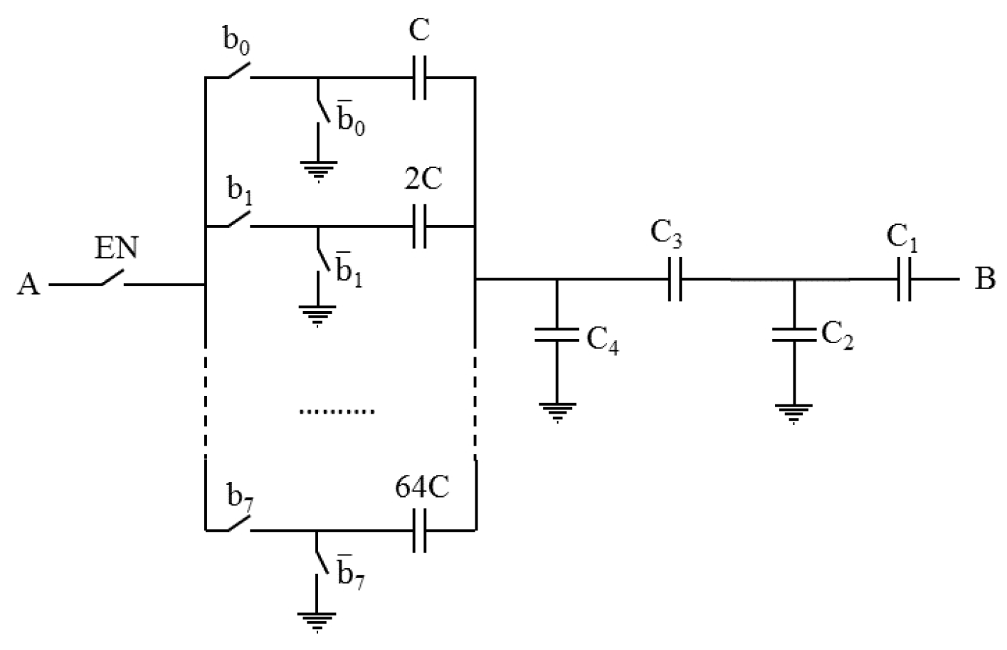
One of the potential problems which may occur during MEMS fabrication is the post-manufacturing capacitance mismatch. Even a relatively small mismatch between top and bottom MEMS capacitors
and
may cause the saturation of the output of the readout circuit, which would effectively render the entire readout circuit unusable. Therefore, a special mismatch compensation circuit was designed. It is composed of two digitally controlled (nine bits each) capacitor ladders, which can be connected in parallel to top and bottom MEMS capacitors [
22]. One bit enables the corresponding mismatch compensation circuit (MCC), while the remaining eight bits are used to choose the value of the desired capacitance of the MCC (
Figure 4). In our design, it is possible to compensate the capacitance mismatch up to about 10% of the total MEMS capacitance. For the detailed description of the offset trimming method using the mismatch compensation circuit, please refer to [
24].
The detailed description of the readout circuit was presented in [
25] and is beyond the scope of this paper; the most important things to retain from this section are the following:
4. Measurement Setup and Results
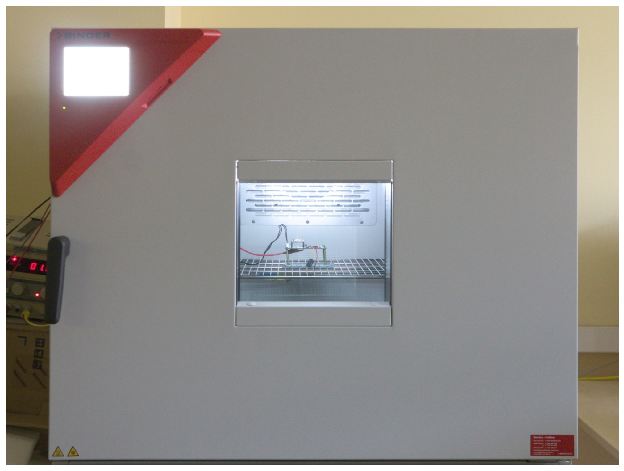
The temperature-related measurements were conducted with the application of an alternating climate chamber Binder MKF 115 E4 partially presented in
Figure 5 during one of the test sessions. The devices under test (DUTs) are specialized test PCB boards. One board is equipped with a complete system (MEMS accelerometer + ROIC) placed in a single QFN-100 package. Another PCB board is equipped with a single ROIC circuit placed in a QFN-100 package.
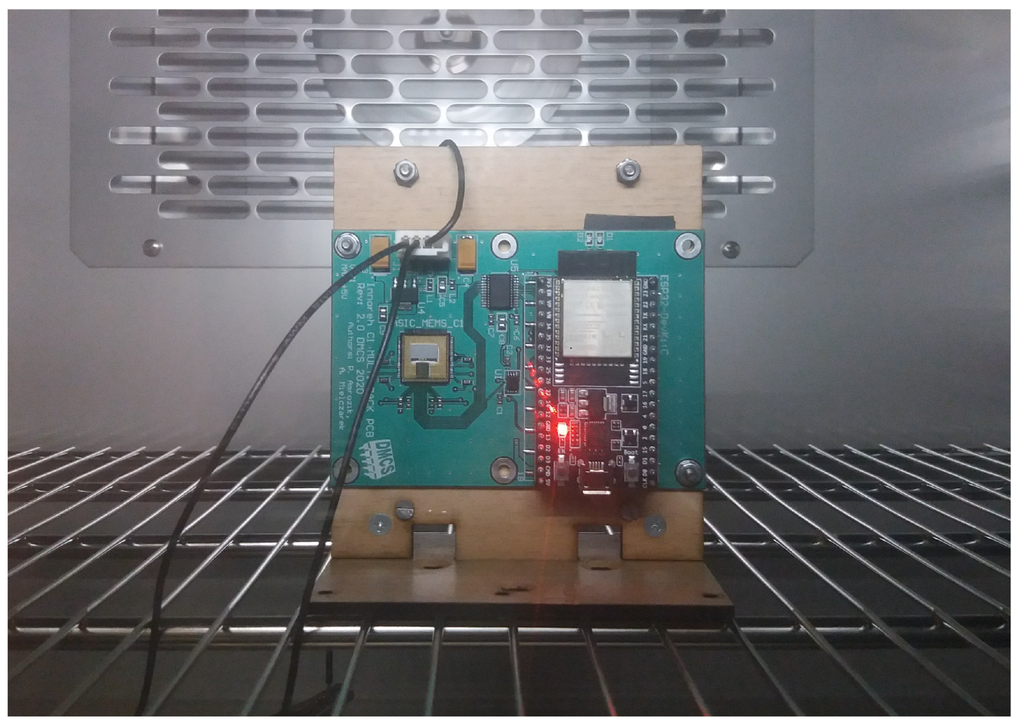
Figure 6 presents the contents of both ROIC and MEMS and ROIC packages. The PCB test boards are equipped with power supply conditioning systems and Wi-Fi communication modules for exchanging information with the ROIC. All ROIC die specimens are identical and each of them is equipped with a 10-bit ADC and a digital signal processing and transmission module. The external Wi-Fi modules used in the test PCB boards are used for programming the ROIC operation, including setup details, and for retrieving the measurement data received by the analog path of the ROIC and processed by its digital part.
Figure 7 presents the test board with MEMS accelerometer and ROIC in a single QFN-100 package. It can be observed that the lid of the package is removed and both structures are visible. Initial test sessions in the climate chamber were performed with an extra protection lid over both structures [
26]. To check the influence of circulating air directly accessing the surfaces of the MEMS and ROIC dies, the package lids were removed.
Figure 8 presents close-ups of both ROIC and MEMS and ROIC measurement setups.
The PCB boards with exposed dies were tested and the results compared with the outcome of previous test sessions. Performed comparison shows that the temperature change during all performed test sessions is so slow that there is no clear and consistent difference in the results obtained for ROIC and MEMS and ROIC setups with and without the protective lid over the QFN-100 package. The lidless setup might be beneficial in case of test sessions with faster temperature changes, but such sessions are not planned. For result consistency, similar speeds of temperature change were used in all performed test sessions.
Figure 8 presents the test board variant with the ROIC-only circuit. In the case of this board, there are no input signals from the MEMS accelerometer, but the ROIC input is not floating. The ROIC is soldered to the test PCB board as shown in
Figure 8 and thus, there are parasitic capacitances connected to all inputs of the ROIC circuit, which stabilize the ROIC input voltage values. These input voltage levels are equalized by the mismatch compensation circuit (MCC) integrated into the ROIC (see
Figure 3). The MCC settings can imitate zero-g input signal (which results in both an input and output voltage of the ROIC close to 2 V) or can imitate other static acceleration values, which is useful for operation comparison of the ROIC-only and MEMS and ROIC PCB test board setups. Such acceleration imitation can be performed by observation of the ROIC output voltage of the ROIC driven by the MEMS working under specific conditions and next manipulating the MCC of the ROIC-only test board setup to recreate the same output voltage values.
Several versions of thermal test procedures have been tried to provide precise measurements of the PCB test boards. During most of these procedures, the PCB test board was heated up to the maximum tested temperature and held in such conditions for about 15 min. Next, the temperature of the climate chamber and the residing test board was slowly decreased in a strictly linear manner. Usually, a decrease of 1 °C was achieved during 3–4 min. Such a temperature change rate was found suitable to enable measurements with a precision comparable to the temperature resolution of the climate chamber itself.
During the original test procedure, the test board remains unpowered by default. It gets powered on only for the duration of a single act of getting measurement data and then gets powered off again. The idea behind such an operation is to limit the extra heating that could alter temperature of the ROIC die from the environment temperature indicated by the climate chamber. To ensure the minimum effect of the ROIC self-heating, constant time periods were kept between consecutive acts of the ROIC measurements. A side effect of this procedure is the fact that if data are collected for small decrements of temperature, constant temperature steps cannot be kept. Durations of single measurement acts were found to vary from less than 10 s to over a minute. Thus, the additional time required for cooling the ROIC after it gets switched off increases the temperature shift between consecutive measurements, which can lead to overshooting limited temperature steps of the originally planned measurement session.
A modified test procedure was proposed, performed, and found suitable for the measurements. During the new procedure, the PCB board remains powered during the whole test session. Temperature decrease is slow and comparable to the one used during the original test procedure. In addition, all lids and caps over the tested structures remain removed to enable access of the airflow to the tested integrated structures.
Figure 7 shows the test board with the MEMS and ROIC structures in a single QFN-100 enclosure with removed lid, during a test session inside the climate chamber. Comparison of the test results showed that the modified test procedure results in very similar measurement results. The new test procedure offers some benefits. First, there is no time loss due to possible prolonged duration of regaining wireless communication with the test board each time after it gets powered on before the next measurement act. Moreover, the utilized version of the test board with the single ROIC requires several supply voltages provided by different devices. Thus, the powering procedure may get more complicated, especially if a specific powering sequence should be kept for securing the safe operation of the test board and all its components. Owing to the test procedure comparison results and virtues of the modified procedure, this one was selected as the default test mode for all the following measurement sessions.
In case of all tried test procedures, the operator of the test process stayed next to the climate chamber and coordinated communications and data retrieval from the test PCB board with the use of a computer connected to the same Wi-Fi network as the test board. There are no means of remote control of the climate chamber, so the operator needs to watch the information (mainly the chamber temperature) presented in the chamber display and initiate a measurement act according to the test session setup.
The measurements were set to be taken in the range of −50 to 100 °C. The upper limit is related to the thermal limitations of the Wi-Fi module and the test board laminate. The lower limit was found rather problematic to be reached and usually the test sessions were terminated in the range from −40 to −45 °C. Reaching temperatures below this range was repeatedly taking increasingly longer times. For this reason, tests for the lowest temperatures were usually cancelled and thus the whole test sessions finished. As a result, the measurements presented in this paper were taken in minimum 5000 sample long series at 1 °C intervals from 100 down to −40 °C.
Most of the measurements presented in this paper were conducted for the MEMS and ROIC structures placed in a single QFN-100 enclosure, presented in
Figure 7. Mainly, the temperature dependence of the MEMS&ROIC system properties and operation was investigated. All measurement results presented and discussed in this paper were conducted using the X-axis accelerometer of the MEMS and the corresponding X-axis channel of the ROIC. The system behavior has been characterized by mean values and standard deviations of all readout series.
The ROIC analog readout path is endowed with a variable gain amplifier, placed just before the integrated ADC (see
Figure 4). This amplifier offers gains equal to 1, 2, 3, 4, 5, 6, 7, and 8. Gain 1 is hard wired (HW) in the output amplifier, while the remaining gain values are defined by a set of CMOS gate switched capacitances in the amplifier signal path. These additional switched capacitances provide gains from 0 (all related switches open) to 7 (all switches closed). Integer gain values of 0 to 7 are set by a 3-bit (B2, B1, B0) control sequence. Most of the temperature-related measurements were taken for gain values equal to: 1, 2, 3, 5, and 8. Such a selection makes possible the extraction of gain components related to each gain control bit. Hard wired gain = 1 is obtained for the control sequence equal 0 (000). The switched gains related to the control bits B0, B1, and B2 are obtained for the control sequences equal respectively 001, 010, and 100, reduced by the HW part of the gain. Thus, gainHW = 1, gainB0 = 2-1, gainB1 = 3-1, gainB2 = 5-1, and as a consequence gainMAX = gainHW + gainB0 + gainB1 + gainB2 = 8.
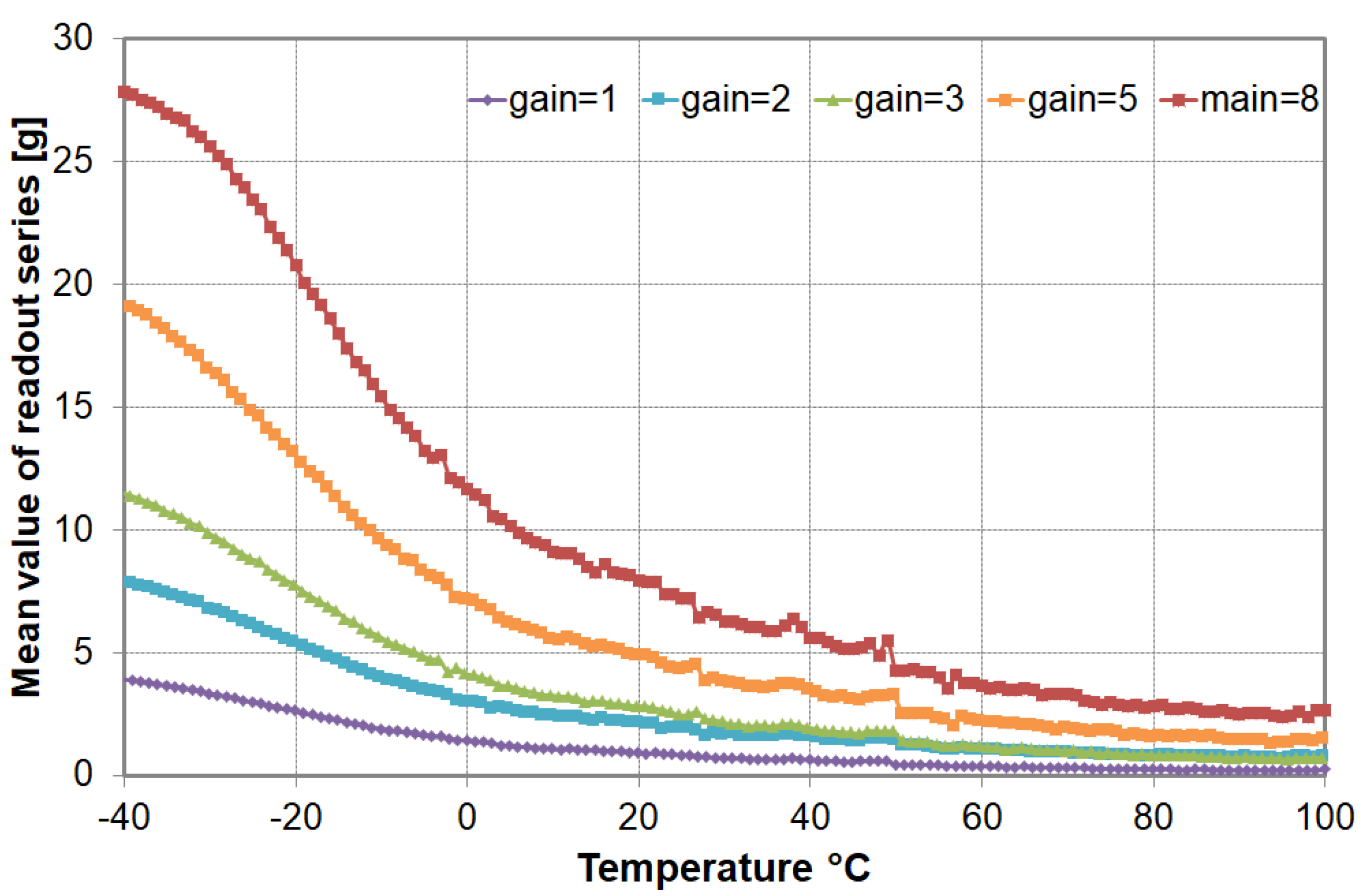
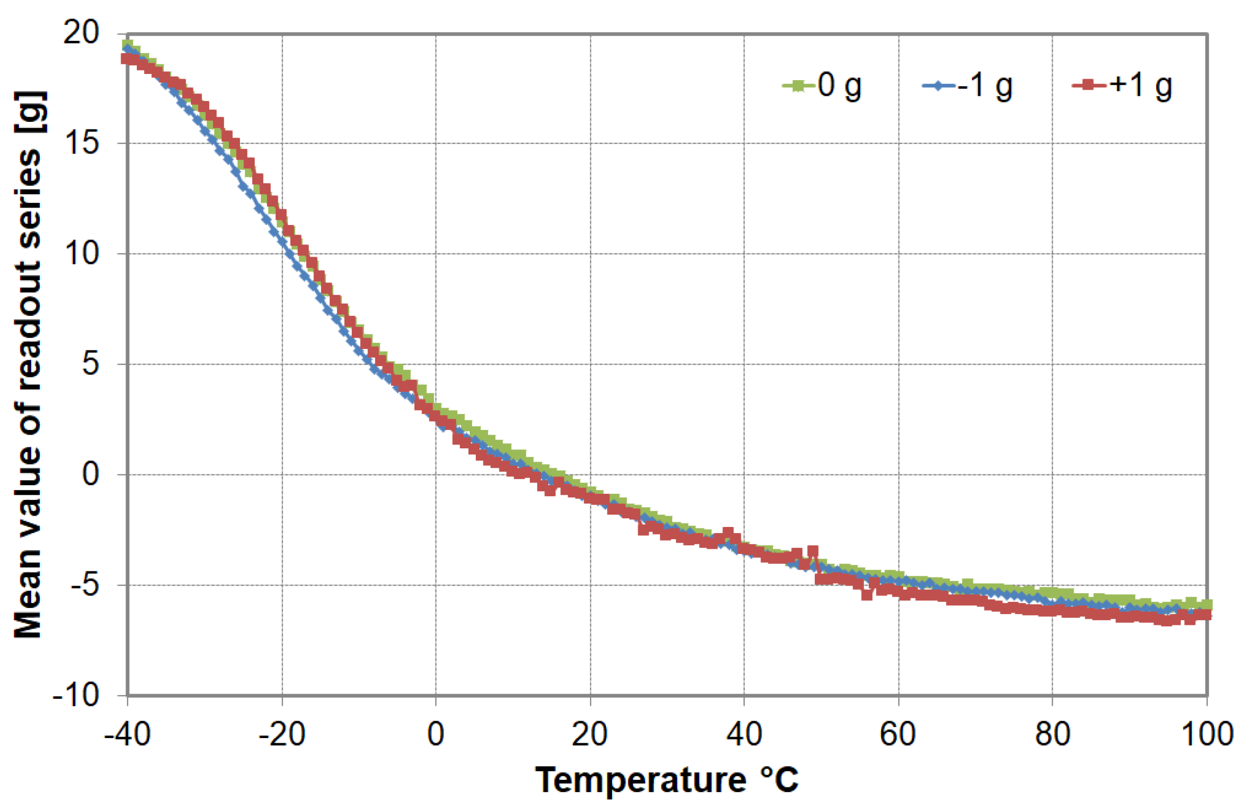
Figure 9 presents the temperature dependence of the mean readout values with selected MSR gain (=1, 2, 3, 5, 8) values for static 0 g acceleration.
The circuit has been tuned at room temperature, which can be seen as a crossover point for all the curves presented in the figure. The presented readouts are scaled to an equivalent acceleration, based on the MEMS sensitivity and at room temperature. It can be observed that the temperature dependence is monotonic in the whole examined temperature range and it falls with temperature, although this dependence is most prominent for negative temperatures. Similar sets of curves were obtained for constant accelerations equal to −1 g (
Figure 10) and 1 g (
Figure 11).
Figure 12 presents the temperature dependence for constant acceleration 1, 0, 1 g and maximum analog gain equal to 8. Distances between the curves for −1 and 0 g accelerations seem to be slightly different than in the case of 0 and 1 g ones. This feature might suggest the nonlinear operation of the analog signal path of the ROIC, but the real cause of this effect is different. Measurements for each or constant acceleration values were obtained during separate measurement sessions. Each of these sessions has been preceded by its own tuning of the ROIC input capacitance imbalance with the integrated trimming circuitry (see
Figure 3 and
Figure 4). Each trimming may lead to slightly different results, as the trimming circuitry has limited precision of adjustment. Measurements taken as a function of a tilt angle and gravitational acceleration presented in [
21] show a high degree of linearity of the MEMS and ROIC system operation. For a more precise shape comparison, the curves for acceleration equal to −1 and 1 g of this figure were shifted and overlapped with the curve for 0 g acceleration, and the resulting curves are presented in
Figure 13. It can be observed that the main difference between these three curves is the shift in the acceleration space and not the curve shape itself. This is one of the signs of the proper operation of the analog signal path of the ROIC.
Figure 14 shows the contribution of each analog gain ingredient (hard wired and set by gain control bits 0, 1, and 2), as presented earlier in this chapter. These contributions are shown per gain unit for direct comparison’s sake. The comparison shows the satisfying quality of the circuit operation.
Measurements for each temperature are taken as a series of readout samples and some noise-related statistical effects can be observed.
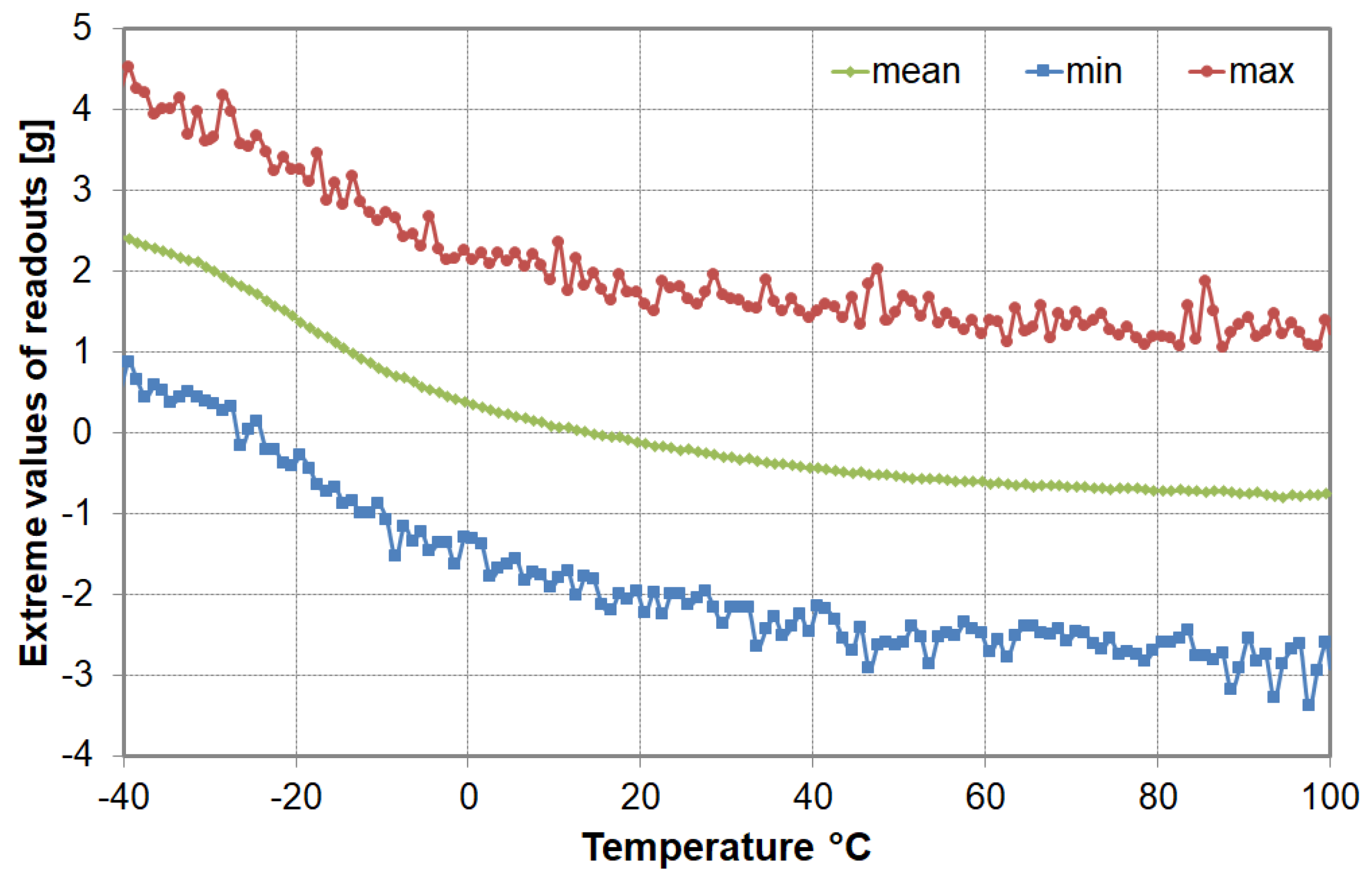
Figure 15 presents the minimum, mean, and maximum values of measurements per gain unit for all examined temperatures. It must be remembered that the minimum and maximum values are extreme readouts for 5000 sample sets.
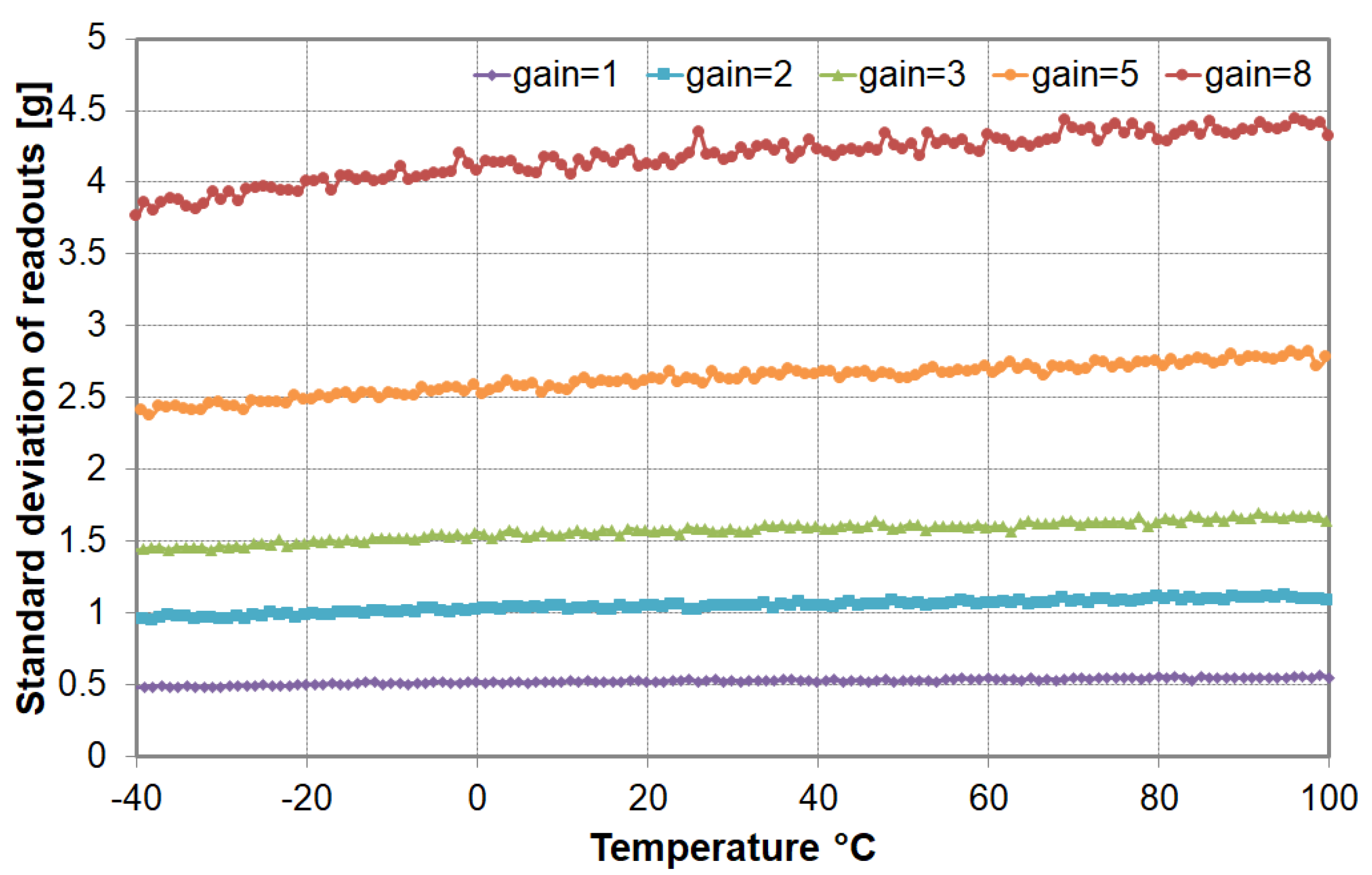
The statistical effects can be better presented by, for example, standard deviation values. The temperature dependence of the obtained standard deviation for all examined gain values and constant acceleration of 0 g are depicted in
Figure 16. Standard deviation values for all gain values are monotonic in the entire examined temperature range and increase with temperature.
Comparisons of standard deviation values per gain unit for measurements taken with accelerations equal to −1, 0, and 1 g are presented in
Figure 17. The curves are nearly overlapping except for the lowest temperature range. There, the curves are based on measurements taken for the highest analog gain of eight and, in the case of acceleration equaling 1 g, some number of readout samples exceeds the maximum conversion voltage of the integrated ADC. The analog readout path can produce an even higher output voltages, but due to its limited quality of operation in a voltage range close to the positive supply voltage range and due to the voltage requirements of the ADC itself, a specific upper readout limit lower than the supply voltage has been set. This effect of standard deviation reduction for low temperatures is directly caused by cutting the excessive analog output voltages to the upper ADC conversion readout limit. The application of specific statistics tools (applicable if not the entire sample distribution is available) might alleviate this effect. On the other hand, the observed effect is a very handy indicator of whether there are any range-related problems with the conversion of analog output voltages to their digital representations.
Figure 18 shows the standard deviation contribution of each analog gain ingredient (hard wired and set by gain control bits 0, 1, and 2), as presented earlier in this section. These contributions are shown per gain unit for direct comparison’s sake. The comparison shows the satisfying quality of the circuit operation. The overlapping of these curves points to the linear progress of standard deviation values with the analog gain of the ROIC.
The complete sensing and readout system consists of the MEMS and ROIC, and knowing the source of all temperature and noise-related effects observed during the measurements is very beneficial.
Figure 19 presents a comparison of the temperature dependence of mean readout values per gain unit for the MEMS and ROIC system placed in a single QFN-100 enclosure and for three ROIC-only setups with no MEMS present. It can be seen that the temperature dependence for the MEMS and ROIC system is at least one order of magnitude stronger than in the case of any of the examined ROIC-only setups.
Figure 20 presents the close-up of temperature dependence for the ROIC-only setups. The presented dependencies discernibly vary. ROIC_1 shows a less significant one than observed in the case of ROIC_2 and ROIC_3 circuits. All ROIC-only setups were tested with the use of PCB boards based on the same project. However, the ROIC_1 was tested on a PCB board specimen manufactured by a different provider than in the case of ROIC_2 and ROIC_3 circuits. The differences observed for all ROIC setups are minute in comparison to those obtained for the MEMS and ROIC setup.
It is a significant clue that points to the MEMS as a source of observed temperature-related effects. Moreover, all the examined ROIC-only setups are equipped with chips fully soldered to their relevant PCB boards. That means that, although the ROIC analog path inputs are not connected to any MEMS, they are connected to the PCB lines and are prone to all related parasitic effects and electrical disturbances.
Figure 6 shows one of QFN-100 packages with the ROIC inside. It can be observed that the ROIC analog inputs are connected to PCB lines leading to the MEMS footprint. On the other hand, the MEMS and ROIC system is placed in a single enclosure and the pads of MEMS and ROIC dies are directly (die-to-die) connected with golden wires only (
Figure 6). Similar effects can be observed in the case of standard deviation value investigation.
Figure 21 shows temperature dependence of standard deviation for all already mentioned setups (one MEMS and ROIC and three ROIC-only). Measurements of the MEMS and ROIC system come with standard deviation values about 2.8 times higher than in the case of any ROIC-only setup. Such higher standard deviation can be explained by the mechanical noise (brownian noise) of the MEMS sensor, which obviously does not exist in the ROIC-only setup. A higher value of noise of course directly affects the variation of the output, increasing the standard deviation of the measurements.
Close-up comparison for all three ROIC-only setups is as presented in
Figure 22. All three curve shapes are reasonably consistent and similar.
Again, also in the case of noise-related dependencies, both the intensity and temperature dependence of the encountered effects are mainly related to the presence of the MEMS capacitances at input of the ROIC analog path and the interconnections of these two structures.
5. Software Simulations
To understand the influence of temperature on the output of the accelerometer, we performed coupled, thermo-electrostatic-mechanical simulations of the accelerometer model shown in
Figure 23. We simulated the accelerometer’s output, i.e., the difference between accelerometer capacitances
=
−
as a function of various parameters and the influence of temperature was modeled by including a coefficient of thermal expansion (CTE) of silicon in the model. We concentrated on modelling the mismatch-induced temperature drift, i.e., the drift caused by the fact that the values of MEMS capacitances
and
are not equal due to the imperfect manufacturing process.
It has to be emphasized that the displacement of the proof mass is usually very small and therefore, the value of
is also very low. As a result, if default meshing methods are used, the different mesh on
and
fingers may result in numerical errors of the same order as the output signal, making it impossible to get the correct accelerometer’s response. To eliminate this effect, it was ensured that the same symmetrical mesh is used on both top and bottom part of the accelerometer [
27]. By applying a zero acceleration to the structure, we ran the simulations and it was verified that the obtained
was equal to zero in that case, as should be expected.
Furthermore, displacement boundary conditions in thermal expansion simulation may induce additional stress that may affect the correct value of capacitance. Thus, the model was equipped with four symmetrically located bars. Prescribed displacement values were applied to the bars ends to ensure that additional stresses appear in bars only.
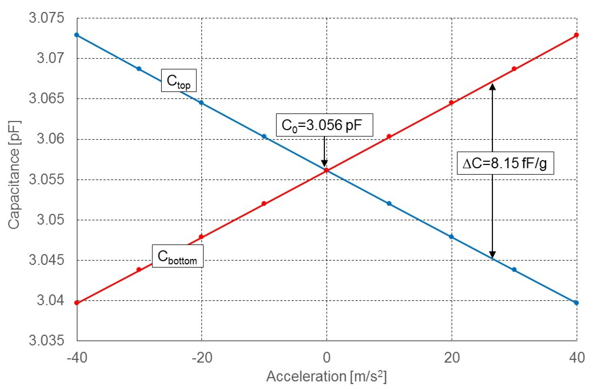
The obtained value of static (zero-g) capacitance was
=
= 3.056 pF and correlates very well with the value obtained via measurements (
= 3.07 pF). The accelerometer’s model output response was linear in the analyzed range and its sensitivity was found to be 8.15 fF/g (see
Figure 24).
However, the initial temperature-sweep simulation showed that the impact of temperature on the output is suspiciously low. The reason is that, in the idealized simulation model, the structure is perfectly symmetrical, = and, moreover, any dependence on temperature is the same for and and gets compensated at the output, as = – . This is of course not the case in real life, due to the stress induced during the manufacturing process, there may be quite a considerable mismatch between and capacitors. This in turn induces the dependence of on the temperature. Let us assume for the sake of argument that, due to post-manufacturing mismatch, is larger than . Then, the value of will rise proportionally more with temperature than , causing a temperature-induced at the output.
Consequently, it was decided to add in the model the post-manufacturing mismatch as a configurable parameter. The mismatch between
and
was achieved by changing the distance between the fingers in the
capacitor. Such a displacement, named
d, caused a change in the value of the
capacitor. Since the value of
remained unchanged, as a result we obtained a non-zero initial value of
, equivalent to the one caused by the potential post-manufacturing mismatch. Considering that those changes of the distance were very small, it can be assumed without making a significant error that the dependence of
on the mismatch
d is linear, that is, a 1% change in
d will cause a 1% change of
at the output. Finally, the simulations were run with both temperature and the initial mismatch as variables.
Table 2 and
Table 3 list the most important simulation parameters.
Figure 25 presents how the value of the output,
, changes with temperature for various values of initial mismatch
d. However, to make things clearer, we subtracted the initial value of
for each displacement, namely
, from each result. In other words, each point in the graph shows how much
changes with temperature with respect to the initial capacitance
. For zero displacement, the slope is naturally close to zero (as the structure is fully symmetrical), but for increasing initial displacement, it increases proportionally to the mismatch and reaches even −2.73 fF/(100 °C) for the displacement of 125 nm. It means that a relative change in the distance between capacitor plates of 125 nm/ 2 μm = 6.25% increased the accelerometer’s sensitivity to temperature by −2.73 fF/(100 °C). Additionally, in
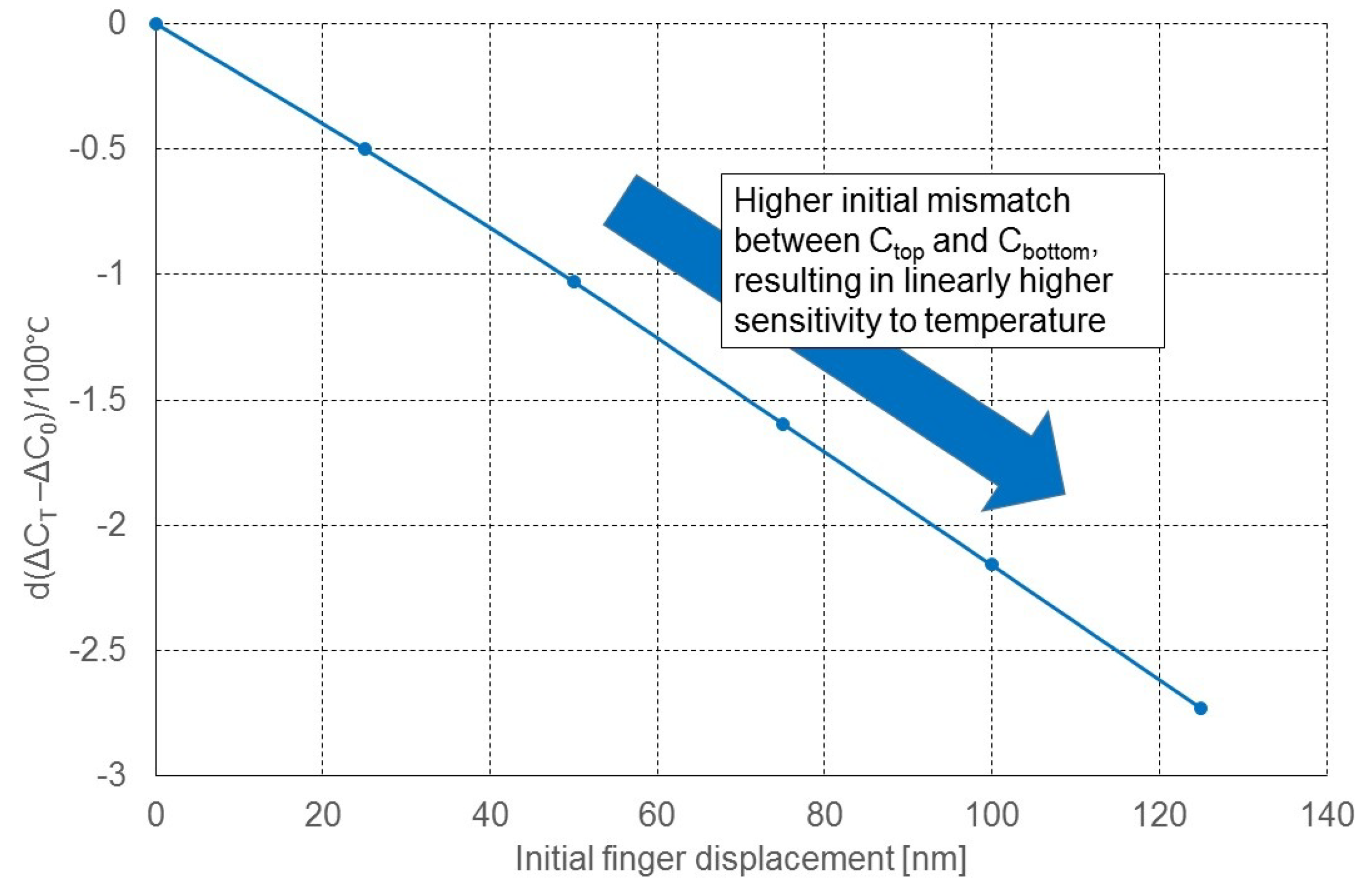
Figure 26, we traced the accelerometer’s sensitivity to temperature (in fF/(100 °C)) as a function of initial finger displacement (artificially-induced mismatch). The dependence is very linear, which allows the introduction of a simple coefficient, which describes the dependence of temperature drift on the initial mismatch (see
Section 6).
6. Discussion
Figure 27 shows how a mismatch compensation circuit can be used to make sure that the post-manufacturing mismatch
does not saturate the output of the readout circuit. By adding a digitally-controllable capacitance in parallel to
, both capacitances seen by the readout circuit, namely
and
, can be equalized. Thus, for zero-g acceleration, the output of the differential readout circuit will be biased exactly at the middle of its range.
Let us now consider the temperature drift of the MEMS capacitors. The problem is that if output is perfectly compensated,
at temperature
, when the temperature changes, both
and
will change proportionately, but
will not change almost at all (the measurements showed that the temperature sensitivity of the MCC is almost negligible, see
Section 4). Consequently, the temperature drift will affect the output and its impact will depend on the initial mismatch
. Let us calculate the difference between
and
for the temperature
.
where
denotes the capacitance at the temperature
. Then, denoting
as the CTE of silicon, and assuming that the circuit was perfectly compensated at
and the fact that
does not depend on the temperature, we get:
Thus, we can conclude that the capacitance difference at the output depends linearly on
, the initial mismatch between
and
capacitors. This confirms that the analytical calculations match the linear dependence shown in
Figure 26.
Let us now discuss the potential impact of the temperature drift on the accelerometer. According to our simulations, the sensor’s sensitivity to acceleration was 8.15 fF/g, while for example, for the finger displacement of 125 nm (6.25% relative mismatch between
and
), the temperature drift was 2.73 fF/(100 °C). In other words, a 6.25% relative mismatch caused the temperature drift, which resulted in the temperature change of 1 °C having the same effect as the acceleration of 3.35 mg. Consequently, as all those dependencies are linear, we can introduce an error parameter
which describes the behavior of the accelerometer due to the temperature drift caused by the mismatch. This parameter conveniently shows the error of the accelerometer’s output caused by the mismatch-induced temperature drift per each percent of relative mismatch and per each degree Celsius. In our case, this parameter was equal to 0.536
.
Let us now compare the above calculations with the measurement results shown in
Figure 9. The first difference is that the measured dependence of the sensor’s output on the temperature was non-linear, which indicates that simulations did not take into account all temperature-dependent effects. One of these effects can be residual stress caused during the manufacturing process by the cooling of the structure after bonding or thin-film deposition. The higher the difference between the operating temperature and thermal process temperature, the higher the residual stress. Consequently, due to this effect, for lower temperatures, the effective structure mismatch will increase, causing a higher thermal drift. Since the simulations were performed for a constant initial mismatch, they did not take into consideration the impact of the residual stress change with temperature. Therefore, this effect is not present in the simulations, but it can be clearly seen in the measurement results: in
Figure 9, the slope of the curves (or temperature sensitivity) increases as the temperature decreases.
According to the measurements, the initial mismatch of the manufactured MEMS structure (compensated using the mismatch compensation circuit) was around 2.2%. Using this value in Equation (
4) allows the calculation that the mismatch-induced temperature drift due to the temperature change from 0 °C to 100 °C should be equal to around 0.12 g. Meanwhile, according to the measurements, the absolute change of the output due to the temperature change from 0 °C to 100 °C was found to be around 2 g (see
Figure 9, the curve for gain = 1). Thus, 6% of the temperature drift in that range was likely caused by the mismatch-induced drift, while the remaining 94% must have been caused by other phenomena not included in the simulations.


 ,
, 


