Article

Gate Current in p-GaN Gate HEMTs as a Channel Temperature Sensitive Parameter: A Comparative Study between Schottky- and Ohmic-Gate GaN HEMTs

Department of Electrical Engineering and Information Technologies, University of Naples Federico II, 80125 Naples, Italy
*
Author to whom correspondence should be addressed.
Energies 2021, 14(23), 8055; https://doi.org/10.3390/en14238055
Submission received: 15 October 2021 / Revised: 24 November 2021 / Accepted: 26 November 2021 / Published: 2 December 2021
(This article belongs to the Special Issue Safety Design and Management of Power Devices including Gate-Drivers)

Abstract

:
In this work, a comparison between the gate-driving requirements of p-GaN HEMTs with gate contact of Schottky and Ohmic type is presented. Furthermore, the presence of a gate current of different magnitude is experimentally verified for both types of devices. Successively, the possibility of using the gate current as a temperature-sensitive parameter and its monitoring during real circuit operation is proposed. The viability of monitoring the gate current without introducing additional complexity in the gate driver is examined through experimental measurements on commercially available p-GaN HEMTs.

1. Introduction

Gallium Nitride (GaN) is a III-V wide-bandgap compound semiconductor exhibiting excellent properties for high-temperature and high-frequency power electronics applications [1]. At present, the most adopted GaN-based power device is the GaN-on-Si lateral high electron mobility transistor (HEMT). In it, the current conduction occurs in a highly conductive electron gas confined in a narrow region beneath the AlGaN/GaN hetero-interface (2DEG, i.e., two-dimensional electron gas). To yield greater intrinsic safety to power-switching systems, the active devices of which they are made are usually required to be normally-off, (i.e., to have a positive threshold voltage, VTH). However, since the 2DEG is inherently present at the AlGaN/GaN hetero-interface, even when no gate bias is supplied, the resulting HEMTs are innately normally-on devices (also referred to as depletion-mode devices) [2]. To overcome this problem and achieve an enhancement-mode behavior, multiple solutions have been proposed in the literature. One option is the recessed gate [3,4], which consists in reducing the thickness of the AlGaN barrier layer beneath the gate contact. Another possibility is the treatment of the gate region with negative fluorine ions [5,6]. The joint effect of both gate recession and fluorine implantation was also investigated [7]. A different approach is that of realizing a cascode configuration by connecting in series a low-voltage enhancement-mode Si MOSFET and a high-volage depletion-mode GaN HEMT [8,9]. A further solution is the introduction of a p-GaN cap layer between the gate contact and the AlGaN region [10]. The latter is the technological choice currently adopted by most manufacturing companies and, except for cascode devices, GaN HEMTs of such a kind are of common commercial availability. Despite the normally-off characteristic, the gate contact of p-GaN gate HEMTs is not isolated as in a conventional MOS-based transistor, thus causing the absorption of a gate leakage current. Moreover, depending on the technological and design parameters of the gate stack, two distinct types of gate contacts can arise [11,12], i.e., Schottky and Ohmic contact. What implications the gate current has on the driving circuitry must be understood since the complexity of the gate driver scheme has a relevant impact on the manufacturing cost. On the other hand, tailored and more complex gate drivers can help to exploit the full potential of GaN devices in terms of both efficiency and robustness [13]. Moreover, there is growing interest in smart gate-driving solutions [14,15,16] that can monitor the conditions of the power devices and actuate control algorithms that seek to enhance the system lifetime by reducing over-stress. Several aging and failure phenomena are temperature-induced and some of them might be single-shot events triggered by a sudden fault. Therefore, sensing the channel (or junction) temperature during converter operation with a good degree of time resolution (online sensing) can prove considerably useful. On the other hand, measuring the temperature via an equivalent electrical parameter oftentimes needs to be done in specific electrical conditions and it requires alternation between the normal operation of the converter and a temperature sensing phase.
The main objectives of this paper can be summarized as follows:
(i)
Discussing the requirements of the gate-driver circuit for the two different classes of normally-off GaN HEMTs with p-type gate;
(ii)
Given the sensitivity of the gate current to the channel temperature [17], discussing the viability of using it as a temperature-sensitive electrical parameter (TSEP) and proposing a sensing circuit for its online monitoring.
The structure of this study is organized as follows. The second section introduces the two different types of p-GaN-based gate contacts from a theoretical perspective. The third section illustrates the gate-driving requirements for the Schottky- and Ohmic-gate devices. In the fourth section, the experimental results concerning the possibility of monitoring the gate current during real circuit operation are presented. The fifth section concludes the analysis.

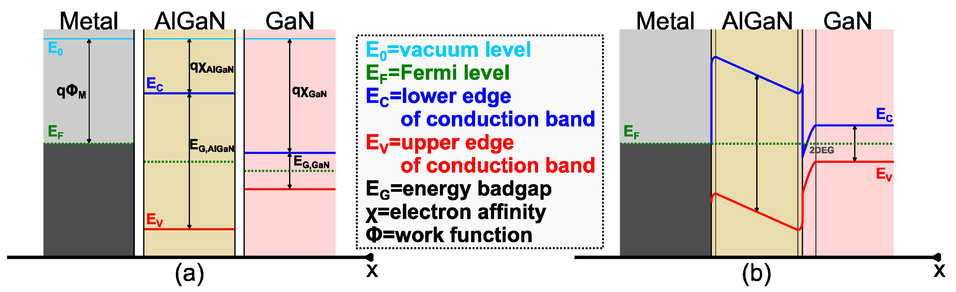
2. Gate Contact Types in Normally-Off p-GaN HEMTs

A well-established type of GaN-on-Si lateral HEMT employs a GaN/AlGaN heterojunction to achieve the formation of the 2DEG, i.e., a shallow sheet of electrons confined in the GaN at the interface with the AlGaN layer. The advantage of having such an electron gas is that it features a conductivity that is much higher than that of the electron in the bulk GaN [18]. Therefore, if a transistor exploits the 2DEG as the conductive channel between source and drain, it will exhibit a very small on-state resistance. However, GaN HEMTs based on the metal/AlGaN/GaN heterostructure usually show a normally-on behavior, i.e., the drain-to-source current conduction is possible even when no gate bias is supplied. The reason behind this can be explained with the help of the idealized band diagram for a hypothetical metal/AlGaN/GaN heterostructure, as illustrated in Figure 1. Figure 1b shows that when the metal/AlGaN/GaN stack is at thermodynamic equilibrium (i.e., the Fermi energy level EF is constant along x), the 2DEG is already formed since the lower edge of the conduction band (EC) lies below EF at the AlGaN/GaN interface. This can be explained by considering that when an AlGaN layer is grown on GaN, a sheet of positive bound charge develops at the AlGaN/GaN interface due to the spontaneous and piezoelectric polarizations induced by the difference between the two materials in terms of polarization field and lattice constant, respectively [19,20]. This results in a strong electric field, attracting a high concentration of electrons to compensate for the positive fixed charge in the AlGaN, thus leading to the formation of a conductive channel also when no gate voltage is provided.
To deplete the 2DEG and make the HEMT normally-off, several solutions have been suggested in the literature [3,4,5,6,7]. Among these, Uemoto et al. proposed to grow a p-doped GaN layer above the AlGaN one [10]. The presence of the p-GaN lifts the lower edge of the conduction band and inhibits the formation of the 2DEG at zero gate bias. The representation of the band diagram reported in Figure 2 helps to visualize this effect. To restore the 2DEG in the metal/p-GaN/AlGaN/GaN stack, a positive gate voltage must be supplied. By doing so, the quantum notch in the GaN layer is shifted below EF and is populated by free electrons.
Depending on the height and thickness of the barrier between EF in the metal and the upper edge of the valence band (EV) in the p-GaN layer, a metal/semiconductor contact with either a resistive or rectifying nature can be obtained. In other words, by properly shaping the Schottky barrier, a HEMT with a Schottky-type or Ohmic-type gate can be manufactured (Figure 3). The main design parameters controlling the shape of the Schottky barrier are the work function of the gate metal (ΦM), the acceptor concentration, and the thickness of the p-GaN layer. Several contributions addressing the single or joint effects of these parameters are available in the literature [11,12,21,22,23]. The choice of these parameters not only determines the type of gate contact but it also affects other device properties, such as the value of VTH, breakdown voltage, and transconductance [11,12]. Consequently, several studies have been focused on finding optimum design criteria [11,12,24].

Experimental Investigation of Gate Leakage Current

The contact formed by the metal/p-GaN junction has a direct impact on the turn-on gate current absorption. If the metal deposited on the p-GaN forms a Schottky contact, then the metal/p-GaN/AlGaN/GaN stack can be modeled by two diodes connected back to back: a Schottky rectifier representing the metal/semiconductor junction and a pn rectifier modeling the AlGaN/GaN interface (Figure 3). In this case, when the gate signal is positive, a limited current flows through the reversely biased Schottky diode (in the order of some µA up to few mA). On the other hand, when the contact between the gate metal and the p-GaN layer is of Ohmic type, the gate heterostructure can be modeled by a resistor and a pn diode connected in series—Figure 3—(the corresponding class of GaN HEMTs is also elsewhere referred to as gate injection transistor). In this case, the gate turn-on current is more pronounced (in the order of some mA up to tents of mA). Although both solutions give a positive VTH, i.e., an enhancement-mode behavior, the magnitude of the gate current has a direct impact on the gate-driving scheme. In this work, the presence of this current was experimentally verified for two different kinds of commercially available GaN HEMTs of similar voltage and current rating. These are a 650 V-30 A-rated GaN HEMT manufactured by GaN Systems (GS66508T [25]) with a Schottky-type gate (this device under test is referred to as DUT_S) and a 600 V-31 A-rated HEMT manufactured by Infineon (IGOT60R070D1 [26]) with a Ohmic-type gate (this device is referred to as DUT_O).
To verify the presence of a gate current (IG) and assess its dependence on the gate-to-source voltage (VGS), the IG-VGS characteristic was measured through the test setup reported in Figure 4, where the voltmeter and the ammeter are two Keithley 2000 bench multimeters. As previously done in [27,28], the IG-VGS characteristic of the DUT_S was measured—Figure 4a—by also connecting in series an external pn diode and while monitoring its voltage drop. The reason for this will be explained in the following sections. For the DUT_O, a current limiting resistor RG = 470 Ω was connected to the gate terminal to avoid damages. For both DUTs, the case temperature was set through a hot plate while the drain and source terminals were connected together to prevent self-heating. The resulting IG-VGS characteristics are reported in Figure 5 and confirm the presence of a current of larger magnitude through the Ohmic gate—Figure 5b—compared to the one through the Schottky gate—Figure 5a. Nevertheless, in both cases, IG has a remarkable dependence on VGS and, more importantly, it exhibits a positive variation with the junction temperature of the device. Having a measurand with a consistent and monotonic dependence on the temperature constitutes the first requirement to make it a feasible TSEP. However, the data of Figure 5 were obtained with short-circuited drain and source terminals and do not account for possible variations in the gate current induced by the drain and source potentials [29,30].
Having the possibility of sensing the gate current during real circuit operation without complicating the gate driver network and without affecting the switching performance constitutes a major advantage. Therefore, for the DUT_S, we propose to monitor IG as the voltage drop on a diode in series with the gate—Figure 4a—and, for the DUT_O, the voltage drop on the RG resistor—Figure 4b. As will be clarified in the following, these components are already present in the conventional gate-driving networks for the respective devices. To estimate the temperature sensitivity of the two different cases, the voltage drops on both the diode (VAK) and on the series resistor RG (VRG) are reported in Figure 6 as a function of the device temperature at various fixed values of VGG. Both VAK and VRG linearly depend on the temperature of the DUT in the explored range of voltage and temperature but VRG(TDUT_O) shows a more pronounced slope (≈2.5 mV/K) than VAK(TDUT_S) (≈1.3 mV/K). The positive variation of the IG as a function of the temperature hints that such a current can be used as a temperature-sensitive parameter for both types of devices when no drain-to-source voltage is supplied. Although encouraging, this electrical condition is unrealistic and it is important to understand whether IG shows a consistent temperature dependence also under drain-to-source bias.

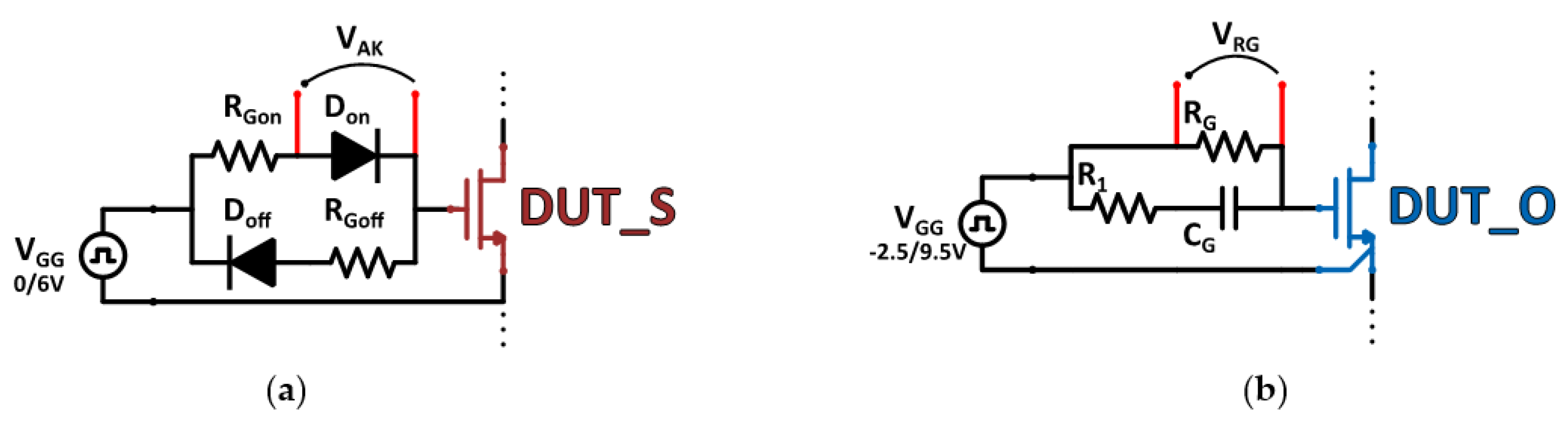
3. Gate-Driving Circuits for Schottky- and Ohmic-Gate p-GaN HEMTs

The different levels of current absorption of the Schottky- and Ohmic-gate contacts require different gate driver networks to optimally control the corresponding classes of devices.
Given the small current flow through the Schottky contact, this category of GaN HEMTs can be considered to be voltage-driven and is compatible with standard (MOSFET-like) gate drivers. A basic scheme of a driving circuit is depicted in Figure 7a [31]. In this topology, the charge and discharge of the gate capacitance happen via two symmetrical and independent branches: one consisting of RGon and Don and the other consisting of RGoff and Doff. Having two separate paths allows usto individually control the slew rate of the gate voltage at turn-on and at turn-off via the resistors RGon and RGoff, respectively. To achieve this, only one of the two diodes (Don or Doff) is sufficient. Nevertheless, placing the diode Don enables us to measure the gate current during the on-time, as highlighted in the previous section. Since it has been previously reported that a gate voltage stress might result in a shift in VTH for this type of transistor [32,33,34,35,36], a clamping diode might optionally be placed between the gate and source terminals to limit the overvoltage.
On the other hand, the higher gate current required by Ohmic-gate HEMTs makes these devices current-driven ones. A basic gate driver network for such devices is sketched in Figure 7b. The role of the capacitance CG is twofold: (i) it provides the current spikes (up to few A) during the turn-on and turn-off transients and (ii) it keeps the gate negatively biased during turn-off, thus decreasing the chances of false turn-on events. Once CG is charged, the gate current decreases to a steady-state value determined by RG. Therefore, for Ohmic-gate HEMTs, the IG slew rate at turn-on and turn-off is controlled by the R1-CG branch, while the on-state IG is provided by RG. Since typical values of driving voltage (VGG) are around 9 V and the on-state gate current is around 10 mA, the value of RG should be selected in the range of hundreds of Ω [37,38]. Given the values of RG and IG, a voltage drop of a few volts will develop across RG. In addition to the basic gate-driving requirements, a more complex network can be designed to optimize the switching performance and the robustness of the devices [13].

4. Experimental Results

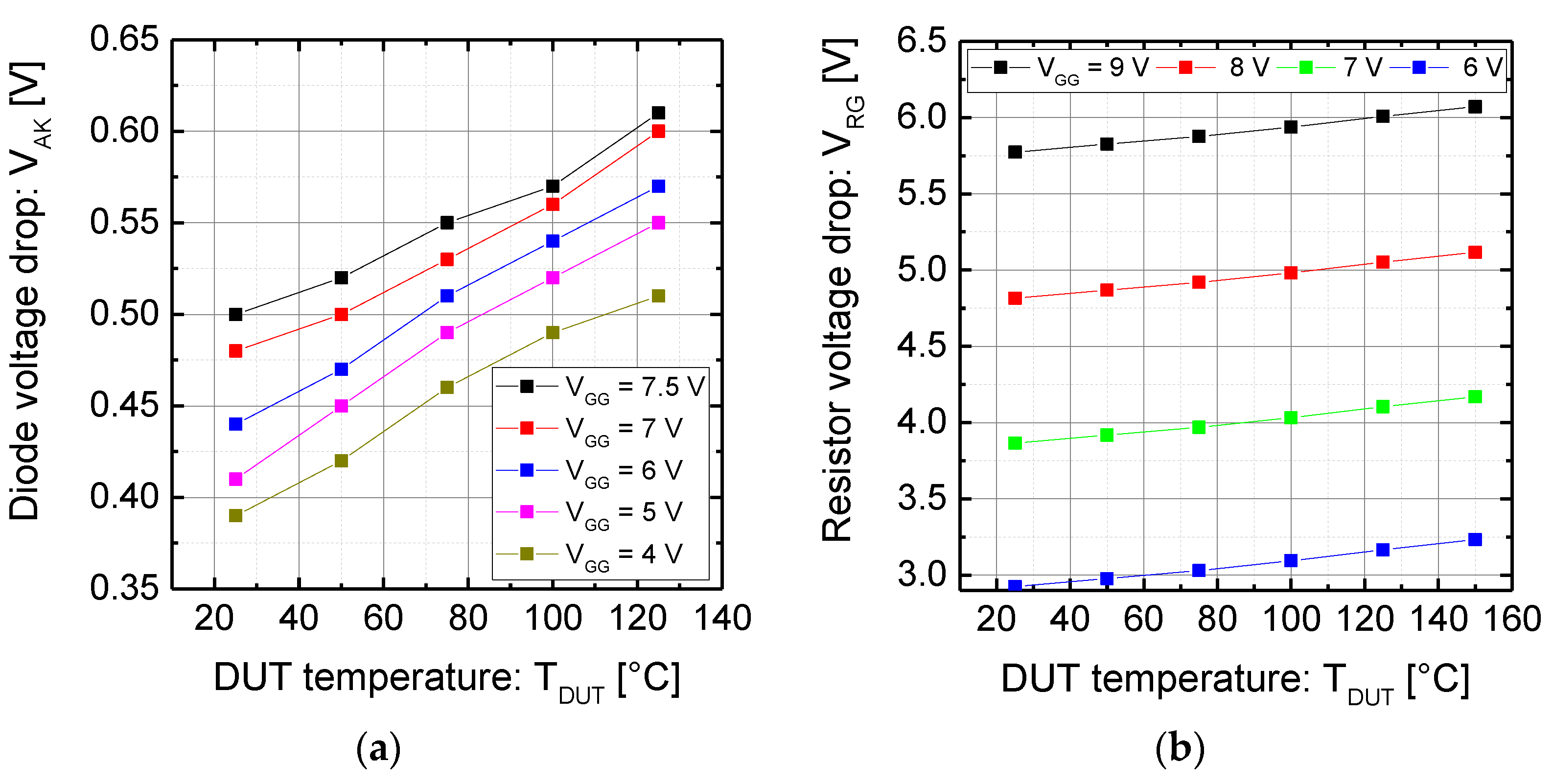
4.1. Gate Driver Circuit for Schottky-Gate p-GaN HEMTs and Monitoring of Gate Current

In a previous work [28], the concept of using IG as a TSEP for Schottky-gate p-GaN HEMTs was introduced and its applicability was tested during real circuit operation. The results of this analysis are briefly recalled in this section to draw a comparison with results related to the Ohmic-gate GaN HEMT. The gate driver of Figure 7a was equipped with a differential amplifier for sensing the voltage drop across the diode Don. The so obtained gate driver and sensing circuit are shown in Figure 8a. The output of the operational amplifier was fed to an RC-envelope detector to smooth the commutations of the output signal attributed to the switching nature of the input VAK. This gate driver network was used to drive the Schottky-gate GaN HEMT (GS66508T) serving as a switch in the prototype boost converter outlined in Figure 8a. To modulate the power dissipated by the DUT_S and, consequently, to vary the steady-state temperature reached by the device, various acquisitions were performed at different steps of switching frequencies. For each tested frequency, the converter was operated until a steady-state electrothermal condition was reached, with a duty cycle of 50% and a DC input voltage Vin = 100 V. The results reported in Figure 8b show that an output signal of the sensing circuit with a higher amplitude corresponds to increasing values of switching frequency.
To study the response of the gate driver and sensing circuit also to abrupt changes in the temperature of the device, the DUT_S was subjected to short circuit pulses of 10 µs with an increasing supplied DC voltage. A schematic representation of the test setup is reported in Figure 9a, while Figure 9b,c report the experimental waveforms of the drain current and the output of the sensing circuit. In particular, the latter reaches higher levels at higher test voltages and it has faster growth during the first phase of the short circuit pulse, i.e., when the current peak occurs. The outcomes reported in this section support the possibility of adopting IG as a TSEP for Schottky-gate GaN HEMTs since it exhibits a monotonic increasing variation with the channel temperature, both during tests at low VDS and high ID (converter operation) and during tests at high VDS and high ID (short circuit operation). However, to relate the value of IG to the actual temperature of the DUT, a further calibration phase is necessary, and it needs to be performed during real operation of the device.

4.2. Gate Driver Circuit for Ohmic-Gate p-GaN HEMTs and Monitoring of Gate Current

A testing plan similar to the one followed for the DUT_S was adopted also for the DUT_O. First, the feasibility of monitoring the gate current and using it as an indicator of the temperature of the DUT_O was experimentally tested within the safe operating area (SOA). For this purpose, the synchronous boost converter sketched in Figure 10 was utilized. It consisted of a half bridge where two DUT_Os were connected in parallel per switching side. The details of the converter are reported in Table 1. In this case, the adopted gate driver slightly differs from the one reported in Figure 7b for the presence of common mode inductors connected between the gate and the Kelvin-source terminals. This helps in damping high-frequency oscillations arising from circuit asymmetries and stray components [39].
To avoid shoot-through, a dead time of around 200 ns was kept between the commutation edges of the VGS of the high-side and low-side DUT_Os. In this case, the modulation of the power dissipated by the DUT_Os was achieved by a variation of the converter input DC voltage. Since no heatsink was placed on the DUT_Os, the supplied voltage was kept well below the voltage rating of the devices to prevent overheating. Figure 11a reports the output voltage of the converter at different values of input voltage. The corresponding waveforms of the voltage drop (VRG) across the resistor RG of the HS1 device are reported in Figure 11b,c.
An increase in VRG from ≈4.2 V to ≈4.6 V was observed as a function of the converter output power.
Successively, the circuit was rearranged as shown in Figure 12a to perform short circuit tests with a pulse width of 10 µs. Moreover, in this case, the power dissipation was varied by increasing the test voltage and, in order to avoid the destruction of the device, it was swept in a relatively low range spanning from 10 V to 60 V—see Figure 12b,c. The insurgence of sustained high-frequency oscillations at VDC = 60 V prohibited us from further increasing the test voltage. Contrarily to what was observed in the previous test, under these circumstances, VRG decreased despite the rise in power dissipation—see Figure 12d. The reason might be attributed to the lateral nature of the GaN HEMTs and to the formation of a high electrical horizontal field when a high value of VDS is applied. Further investigation of the phenomenon is necessary to confirm this hypothesis. For the DUT_O, conversely to what was observed for the DUT_S, IG showed opposite variation depending on the electrical conditions. IG had a positive variation with the power dissipation when the DUT_O was used in a boost converter, while it decreased when the device was subjected to high VDS and ID during the short circuit tests. Therefore, these findings discourage the adoption of IG as a TSEP for Ohmic-gate p-GaN HEMTs.

5. Summary

In this paper, a comparison between the gate-driving requirements of p-GaN HEMTs with Schottky and Ohmic types of gate contact has been presented. The different magnitudes of gate current have been experimentally verified on commercially available devices for the two classes of GaN HEMTs. The strong influence of the temperature on the IG, associated with the monotonic dependence of IG on the temperature when no drain-to-source voltage is supplied, has led to the idea of exploiting it as a TSEP. After considering typical driving circuits for the Schottky- and Ohmic-gate HEMTs, a means of monitoring IG has been proposed for both driving schemes. The sensing elements bring no additional complexity to standard driving topologies and IG can be monitored during regular operation of the device, thus allowing for online estimation of the IG. The experimental results for the Schottky-type gate show that an increase in power dissipation leads to an increase in the IG during tests both in and out of the SOA. On the other hand, the tests conducted on the Ohmic-type DUT highlight that when the power dissipated by the device rises, IG increases when the device is operated as a switch in a boost converter but decreases when the device is subjected to short circuit stress. In conclusion, the variation in IG in a single direction obtained under different test conditions for the Schottky-type gate makes IG a good candidate to be used as a TSEP. For Ohmic-gate GaN HEMTs, this possibility is the hindered by the variations in opposite directions of IG observed during the converter and short circuit operation.

Author Contributions

Conceptualization, A.B., M.R., A.D.C., L.M., G.B. and A.I.; methodology, A.B., M.R. and A.D.C.; validation, A.B., M.R. and A.D.C.; formal analysis, A.B., M.R. and A.D.C.; investigation, A.B., M.R. and A.D.C.; resources, A.B., M.R., A.D.C., L.M., G.B. and A.I.; data curation, A.B., M.R. and A.D.C.; writing—original draft preparation, A.B.; supervision, A.B., M.R., A.D.C., L.M., G.B. and A.I. All authors have read and agreed to the published version of the manuscript.

Funding

This research received no external funding.

Conflicts of Interest

The authors declare no conflict of interest.

References

  1. Meneghini, M.; Meneghesso, G.; Zanoni, E. (Eds.) Power GaN Devices; Springer International Publishing: Cham, Switzerland, 2017. [Google Scholar] [CrossRef]
  2. Yu, H.A.; Duan, T. Gallium Nitride Power Devices, 1st ed.; Pan Stanford Publishing: Singapore, 2017. [Google Scholar]
  3. Kumar, V.; Kuliev, A.; Tanaka, T.; Otoki, Y.; Adesida, I. High transconductance enhancement-mode AlGaN/GaN HEMTs on SiC substrate. Electron. Lett. 2003, 39, 1758–1760. [Google Scholar] [CrossRef]
  4. Saito, W.; Takada, Y.; Kuraguchi, M.; Tsuda, K.; Omura, I. Recessed-gate structure approach toward normally off high-Voltage AlGaN/GaN HEMT for power electronics applications. IEEE Trans. Electron Devices 2006, 53, 356–362. [Google Scholar] [CrossRef]
  5. Cai, Y.; Zhou, Y.; Chen, K.J.; Lau, K.M. High-performance enhancement-mode AlGaN/GaN HEMTs using fluoride-based plasma treatment. IEEE Trans. Electron Devices 2005, 26, 435–437. [Google Scholar] [CrossRef]
  6. Cai, Y.; Zhou, Y.; Lau, K.M.; Chen, K.J. Control of threshold voltage of AlGaN/GaN HEMTs by fluoride-based plasma treatment: From depletion mode to enhancement mode. IEEE Trans. Electron Devices 2006, 53, 2207–2215. [Google Scholar] [CrossRef]
  7. Zhang, Y.; Sun, M.; Joglekar, S.J.; Fujishima, T.; Palacios, T. Threshold voltage control by gate oxide thickness in fluorinated GaN metal-oxide-semiconductor high-electron-mobility transistors. Appl. Phys. Lett. 2013, 103, 33524. [Google Scholar] [CrossRef]
  8. FRoccaforte, F.; Greco, G.; Fiorenza, P.; Iucolano, F. An overview of normally-off GaN-based high electron mobility transistors. Materials 2019, 12, 1599. [Google Scholar] [CrossRef] [PubMed] [Green Version]
  9. Jones, E.A.; Wang, F.F.; Costinett, D. Review of commercial GaN power devices and GaN-based converter design challenges. IEEE J. Emerg. Sel. Top. Power Electron. 2016, 4, 707–719. [Google Scholar] [CrossRef]
  10. Uemoto, Y.; Hikita, M.; Ueno, H.; Matsuo, H.; Ishida, H.; Yanagihara, M.; Ueda, T.; Tanaka, T.; Ueda, D. Gate injection transistor (GIT)—A normally-off AlGaN/GaN power transistor using conductivity modulation. IEEE Trans. Electron Devices 2007, 54, 3393–3399. [Google Scholar] [CrossRef]
  11. Efthymiou, L.; Longobardi, G.; Camuso, G.; Chien, T.; Chen, M.; Udrea, F. On the physical operation and optimization of the p-GaN gate in normally-off GaN HEMT devices. Appl. Phys. Lett. 2017, 110, 123502. [Google Scholar] [CrossRef]
  12. Tokuda, H.; Asubar, J.T.; Kuzuhara, M. Design considerations for normally-off operation in Schottky gate p-GaN/AlGaN/GaN HEMTs. Jpn. J. Appl. Phys. 2020, 59, 084002. [Google Scholar] [CrossRef]
  13. Wu, H.; Fayyaz, A.; Castellazzi, A. P-gate GaN HEMT gate-driver design for joint optimization of switching performance, freewheeling conduction and short-circuit robustness. In Proceedings of the 2018 IEEE 30th International Symposium on Power Semiconductor Devices and ICs (ISPSD), Chicago, IL, USA, 13–17 May 2018; pp. 232–235. [Google Scholar] [CrossRef]
  14. Wang, M.; Zhang, W.J.; Liang, J.; Cui, W.T.; Ng, W.T.; Nishio, H.; Sumida, H.; Nakajima, H. A smart gate driver for SiC power MOSFETS with aging compensation and ringing suppression. In Proceedings of the 2021 33rd International Symposium on Power Semiconductor Devices and ICs (ISPSD), Nagoya, Japan, 30 May–3 June 2021. [Google Scholar] [CrossRef]
  15. Zhang, W.J.; Yu, J.; Cui, W.T.; Leng, Y.; Liang, J.; Hsieh, Y.-T.; Tsai, H.-H.; Juang, Y.-Z.; Yeh, W.-K.; Ng, W.T. A smart gate driver IC for GaN power HEMTs with dynamic ringing suppression. IEEE Trans. Power Electron. 2021, 36, 14119–14132. [Google Scholar] [CrossRef]
  16. Weckbrodt, J.; Ginot, N.; Batard, C.; Azzopardi, S. Monitoring of gate leakage current on SiC power MOSFETs: An estimation method for smart gate drivers. IEEE Trans. Power Electron. 2021, 36, 8752–8760. [Google Scholar] [CrossRef]
  17. Stockman, A.; Masin, F.; Meneghini, M.; Zanoni, E.; Meneghesso, G.; Bakeroot, B.; Moens, P. Gate conduction mechanisms and lifetime modeling of p-Gate AlGaN/GaN high-electron-mobility transistors. IEEE Trans. Electron Devices 2018, 65, 5365–5372. [Google Scholar] [CrossRef]
  18. Kittel, C. Introduction to Solid State Physics, 8th ed.; Wiley Publishing: Hoboken, NJ, USA, 1996; ISBN 978-0-471-41526-8. [Google Scholar]
  19. Bernardini, F.; Fiorentini, V.; Vanderbilt, D. Spontaneous polarization and piezoelectric constants of III-V nitrides. Phys. Rev. B Condens. Matter Mater. Phys. 1997, 56, R10024–R10027. [Google Scholar] [CrossRef] [Green Version]
  20. Ambacher, O.; Smart, J.; Shealy, J.R.; Weimann, N.G.; Chu, K.; Murphy, M.; Schaff, W.J.; Eastman, L.F.; Dimitrov, R.; Wittmer, L.; et al. Two-dimensional electron gases induced by spontaneous and piezoelectric polarization charges in N- And Ga-face AIGaN/GaN heterostructures. J. Appl. Phys. 1999, 85, 3222–3233. [Google Scholar] [CrossRef] [Green Version]
  21. Wu, Y.R.; Singh, M.; Singh, J. Gate leakage suppression and contact engineering in nitride heterostructures. J. Appl. Phys. 2003, 94, 5826–5831. [Google Scholar] [CrossRef] [Green Version]
  22. Fujii, T.; Tsuyukuchi, N.; Hirose, Y.; Iwaya, M.; Kamiyama, S.; Amano, H.; Akasaki, I. Control of threshold voltage of enhancement-mode AlxGa1-xN/GaN junction heterostructure field-effect transistors using p-GaN gate contact. Jpn. J. Appl. Phys. 2007, 46, 115. [Google Scholar] [CrossRef]
  23. Lee, F.; Su, L.-Y.; Wang, C.-H.; Wu, Y.-R.; Huang, J.J. Impact of gate metal on the performance of p-GaN/AlGaN/GaN high electron mobility transistors. IEEE Trans. Electron Devices 2015, 36, 232–234. [Google Scholar] [CrossRef]
  24. Bakeroot, B.; Stockman, A.; Posthuma, N.; Stoffels, S.; Decoutere, S. Analytical model for the threshold voltage of p-(Al)GaN high-electron-mobility transistors. IEEE Trans. Electron Devices 2018, 65, 79–86. [Google Scholar] [CrossRef]
  25. GaN Systems. GS66508T top-side cooled 650 V E-mode GaN transistor. In GS66508T Data Sheet; GaN Systems: Kanata, ON, Canada, 2020; rev. 200402. [Google Scholar]
  26. Infineon. 600V CoolGaN™ enhancement-mode power transistor. In IGOT60R070D1 Data Sheet; Infineon: Neubiberg, Germany, 2020; rev. 2.12. [Google Scholar]
  27. Borghese, A.; Riccio, M.; Longobardi, G.; Maresca, L.; Breglio, G.; Irace, A. Gate leakage current sensing for in situ temperature monitoring of p-GaN gate HEMTs. Microelectron. Reliab. 2020, 114, 113762. [Google Scholar] [CrossRef]
  28. Borghese, A.; Riccio, M.; Maresca, L.; Breglio, G.; Irace, A. Gate driver for p-GaN HEMTs with real-time monitoring capability of channel temperature. In Proceedings of the 2021 33rd International Symposium on Power Semiconductor Devices and ICs (ISPSD), Nagoya, Japan, 30 May–3 June 2021; pp. 63–66. [Google Scholar] [CrossRef]
  29. Fernandez, M.; Perpina, X.; Roig, J.; Vellvehi, M.; Bauwens, F.; Jorda, X.; Tack, M. P-GaN HEMTs drain and gate current analysis under short-circuit. IEEE Trans. Electron Devices 2017, 38, 505–508. [Google Scholar] [CrossRef]
  30. Riccio, M.; Romano, G.; Maresca, L.; Breglio, G.; Irace, A.; Longobardi, G. Short circuit robustness analysis of new generation Enhancement-mode p-GaN power HEMTs. In Proceedings of the 2018 IEEE 30th International Symposium on Power Semiconductor Devices and ICs (ISPSD), Chicago, IL, USA, 13–17 May 2018; pp. 104–107. [Google Scholar] [CrossRef]
  31. GaN Systems. How to drive GaN Enhancement mode HEMT. In Application Note GN001; GaN Systems: Kanata, ON, Canada, 2016. [Google Scholar]
  32. He, J.; Tang, G.; Chen, K.J. VTH instability of p-GaN gate HEMTs under static and dynamic gate stress. IEEE Trans. Electron Devices 2018, 39, 1576–1579. [Google Scholar] [CrossRef]
  33. Gonzalez, J.O.; Etoz, B.; Alatise, O. Characterizing threshold voltage shifts and recovery in Schottky gate and ohmic gate GaN HEMTs. In Proceedings of the 2020 IEEE Energy Conversion Congress and Exposition (ECCE), Detroit, MI, USA, 11–15 October 2020; pp. 217–224. [Google Scholar] [CrossRef]
  34. Zeng, C.; Xu, W.; Xia, Y.; Pan, D.; Wang, Y.; Wang, Q.; Zhu, Y.; Ren, F.; Zhou, D.; Ye, J.; et al. Investigations of the gate instability characteristics in Schottky/ohmic type p-GaN gate normally-off AlGaN/GaN HEMTs. Appl. Phys. Express 2019, 12, 121005. [Google Scholar] [CrossRef]
  35. Shi, Y.; Zhou, Q.; Cheng, Q.; Wei, P.; Zhu, L.; Wei, D.; Zhang, A.; Chen, W.; Zhang, B. Carrier transport mechanisms underlying the bidirectional VTH shift in p-GaN gate HEMTs under forward gate stress. IEEE Trans. Electron Devices 2019, 66, 876–882. [Google Scholar] [CrossRef]
  36. Stockman, A.; Moens, P. ON-state gate stress induced threshold voltage instabilities in p-GaN Gate AlGaN/GaN HEMTs. In Proceedings of the 2020 IEEE International Integrated Reliability Workshop (IIRW), South Lake Tahoe, CA, USA, 4–8 October 2020; pp. 1–4. [Google Scholar] [CrossRef]
  37. Gurpinar, E.; Castellazzi, A. Single-phase T-type inverter performance benchmark using Si IGBTs, SiC MOSFETs, and GaN HEMTs. IEEE Trans. Power Electron. 2016, 31, 7148–7160. [Google Scholar] [CrossRef]
  38. Zojer, B. Driving 600 V CoolGaN™ high electron mobility transistors. In Application Note AN_201702_PL52_012; Infineon Technologies AG: Neubiberg, Germany, 2018. [Google Scholar]
  39. Garcia Mora, R.A.; Haksoz, Y.; Persson, E. How to parallel CoolGaN™ 600 V HEMT in half-bridge configurations for higher-power applications. In Engineering Report V1.0; Infineon Technologies AG: Neubiberg, Germany, 2020. [Google Scholar]
Figure 1. Ideal representation of a monodimensional band diagram of a metal/AlGaN/GaN heterostructure (not to scale) when (a) the three materials are isolated from each other and (b) when the materials are in contact at thermodynamic equilibrium. The correct band bending depends on the exact charge spatial distribution.
Energies 14 08055 g001
Figure 2. Ideal representation of a monodimensional band diagram of a metal/p-GaN/AlGaN/GaN heterostructure (not to scale) at thermodynamic equilibrium. The correct band bending depends on the exact charge spatial distribution.
Energies 14 08055 g002
Figure 3. Ideal representation of the cross-section of the region forming the gate heterostructure in a p-GaN gate HEMT. The equivalent circuits corresponding to the Schottky and Ohmic gate contact types are also reported.
Energies 14 08055 g003
Figure 4. Schematic of the test setup for the static measurement of the gate current as function of the gate-to-source voltage for (a) the DUT with Schottky-type gate and (b) the DUT with Ohmic-type gate.
Energies 14 08055 g004
Figure 5. Experimental gate current at various temperatures as a function of the gate-to-source voltage when drain and source are short-circuited for (a) DUT_S and (b) DUT_O.
Energies 14 08055 g005
Figure 6. Voltage drop (a) on the diode as a function of the temperature on the DUT_S and (b) on the series resistor as a function of the temperature on the DUT_O. The data were measured at different values of gate supply voltage.
Energies 14 08055 g006
Figure 7. Typical gate driver networks for (a) Schottky−gate and (b) Ohmic−gate GaN HEMTs.
Energies 14 08055 g007
Figure 8. (a) Circuit schematic of the prototyped step-up converter based on Schottky-gate p-GaN HEMT and gate driver with the sensing differential amplifier; (b) output waveforms of the sensing circuit at different switching frequencies.
Energies 14 08055 g008
Figure 9. (a) Schematic representation of the setup for short circuit test and corresponding experimental waveforms of (b) the drain current through the DUT_S and (c) the output of the sensing circuit.
Energies 14 08055 g009
Figure 10. Circuit schematic of the synchronous step-up converter based on Ohmic-gate p-GaN HEMTs and of the gate driver.
Energies 14 08055 g010
Figure 11. Waveforms associated with the synchronous step-up converter based on Ohmic-gate p-GaN HEMTs. (a) Output voltage of the boost converter, (b) voltage drop on the gate resistor, and (c) magnified view during the on-phase.
Energies 14 08055 g011
Figure 12. (a) Circuit schematic of the short circuit test setup adopted for the DUT_O and corresponding waveforms of (b) drain-to-source voltage, (c) drain current, and (d) voltage drop on the resistor RG.
Energies 14 08055 g012
Table 1. Main parameters of the DCDC boost converter used for testing the DUT_S and depicted in Figure 10.
ParameterValueUnit
VDC,in20 to 120[V]
fsw500[kHz]
CDC100[µF]
RLOAD50[Ω]
L1240[µH]
RG470[Ω]
CG3[nF]
R110[Ω]
R2, R31[Ω]
Publisher’s Note: MDPI stays neutral with regard to jurisdictional claims in published maps and institutional affiliations.

