
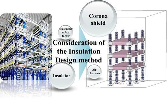
Consideration of the Insulation Design Method on a ±200 kV Converter Valve Unit in an HVDC Converter Hall


1
Department of Electrical and Electronic Engineering, Hanyang University, Ansan-si 15588, Korea
2
Transmission and Substation Lab, KEPRI, Daejeon 34056, Korea
*
Author to whom correspondence should be addressed.
Energies 2021, 14(8), 2296; https://doi.org/10.3390/en14082296
Submission received: 4 March 2021
/
Revised: 9 April 2021
/
Accepted: 15 April 2021
/
Published: 19 April 2021
(This article belongs to the Special Issue Analysis, Design and Optimization of Electric Machines)
Abstract
:A converter valve unit, which converts Alternating Current (AC) to Directing Current (DC) and DC to AC, is one of the key elements of high voltage direct current (HVDC) transmission. The insulation design of a converter valve unit should be considered for air clearance according to the DC superimposed overvoltage and the insulator that maintains the insulation performance and the corona shield to suppress DC corona discharge. There is no prescribed standard for the insulation design of a converter valve unit. Moreover, insulation performance under an applied DC voltage has not yet been thoroughly investigated. Therefore, it is necessary to study the insulation design method of the converter valve unit. In this paper, consideration of the insulation design method on a ±200 kV converter valve unit in an HVDC converter hall is performed. The finite element method (FEM) is used to simulate the 3D model. Additionally, the safety factor () is applied in accordance with the dielectric test in IEC 62271-1. As a result, an insulation design process on the converter valve unit is proposed and the insulation design is carried through the design factors. It is confirmed that design factors on the air clearance, insulator and corona shield have a significant effect on a highly reliable insulation design.
1. Introduction
HVDC transmission lines have a high capacity to transmit electrical power with low power losses and other suitable sustainable transmission properties. Therefore, the planning and implementation of HVDC systems are currently hot research topics [1]. The converter valve unit, which converts AC to DC and DC to AC, is one of the key elements of HVDC transmission. The converter valve unit is made up of several components including thyristors, anode reactors, valve control units, water-cooling equipment, mechanical support devices, insulators, valve arresters, electrical connectors and shielding [2].
Numerous components that can withstand high hybrid AC-DC voltage are assembled in the limited space of converter valve units [3]. The complex structure and high operating voltage may lead to electric field distortions such as the breakdown of overvoltage between the converter valve unit and the wall and ceiling, flashover discharge and surface discharge in the insulator and DC corona discharge in normal operation. DC corona discharge can cause serious accidents during the normal operation of converter valve units [3]. The electrical stress applied between the corona shields to the low voltage part from the high voltage part also shows different distributions due to stray capacitance [4]. If the voltage equalization between the valve modules fails, the converter valve unit may be damaged by the concentration of electrical stress at a specific point [5,6]. For a high reliability of the converter valve unit, the flashover distance and surface distance of the insulator and the air clearance need to be considered and the insulation design of the DC corona shield should also be performed considering the stray capacitance. Design factors of the converter valve unit are the air clearance between the converter valve unit and the wall and ceiling according to overvoltage such as the switching impulse and lighting impulse superimposed with the normal operation voltage, the minimum flashover distance and surface distance and the suppression of the triple point of the insulator and the corona shield to suppress DC corona discharge during normal operation. A well-designed corona shield could improve the electric field distribution of the converter valve unit and minimize the surface field strength on itself [3].
In the Republic of Korea, a ± 200 kV class of DC transmission is being considered as an alternative to the 345 kV class of AC transmission. Moreover, research and development on a ± 200 kV voltage source converter (VSC) and dielectric materials are being carried out as an industry-academic research program. Prior to the research on the converter valve unit, the main research content was only the analysis of the electrical characteristics of the converter valve unit and the electrical characteristics of the converter valve unit were mainly analyzed for the AC/DC superimposed voltage and not the DC superimposed overvoltage [7,8,9,10]. There is also no prescribed standard, method, design process or design factor on the insulation design of a converter valve unit and the dielectric performance under an applied DC voltage has not yet been thoroughly investigated [11]. Therefore, an insulation design process and design factors should be established as well as an analysis of the electrical characteristics of a ± 200 kV converter valve unit for DC superimposed overvoltage.
In this paper, consideration of the insulation design method of a ± 200 kV converter valve unit in an HVDC converter hall is performed. The finite element method (FEM) was used to simulate a 3D model of a ± 200 kV converter valve unit. Additionally, a safety factor () was applied in accordance with the standard on lighting impulse testing in the dielectric test of IEC 62271-1. For an efficient and highly reliable insulation design of the converter valve unit, first the air clearance between the converter valve unit and the wall and ceiling according to the DC superimposed overvoltage is calculated. Second, based on the criterion surface electric field of the polymer material, the minimum flashover distance and surface distance of the insulator is determined when the shield ring is applied for triple point suppression. Finally, based on the criterion electric field on the DC corona discharge, a DC corona shield of the converter valve unit with the air clearance and insulator is designed. At this time, the stray capacitance of the converter valve unit is considered.
2. Insulation Design Process of the HVDC Converter Valve Unit
In this paper, consideration of the insulation design method of a ± 200 kV converter valve in an HVDC converter hall was performed. The HVDC converter valve unit was located in the hall. The insulation components of the HVDC converter valve unit consisted of converter modules, the post insulator between the converter valve and ground and the interlayer insulator between the converter modules and the corona shield. Establishing the insulation design process of the converter valve unit is very important for an efficient insulation design because there are many design factors. Figure 1 shows the insulation design process of the HVDC converter valve unit. First, the air clearance of the converter valve unit was conducted to calculate the insulation distance between the converter valve unit and the wall and ceiling. Second, the insulation design of the insulator was conducted. The maximum surface electric field intensity of a polymer material was calculated and the flashover distance of the insulator was derived to be compact and safe. The shield ring of the insulator was designed to suppress the triple point and cover the X-bar. Finally, the insulation design of the ± 200 kV converter valve unit was performed by applying the insulation distance of the hall and the insulator. The maximum DC corona inception electric field intensity (EDCCI) was calculated through the experiments. Through this, the DC corona shield at the corner, side and shield ring of the top insulator was designed. At this time, the stray capacitance was considered by applying the FEM.
3. SF in Accordance with the Standard of the Dielectric Test in IEC 62271-1
The was adopted to apply the design margin when designing a ± 200 kV converter valve unit. The was given by the following equation [12]:
In Equation (1), represented the maximum electric field intensity at the discharge of dielectric materials for the applied model. represented the maximum electric field intensity of the designed model. When the was ≤ 1, the insulation performance was very unsafe. When the was ≥ 1, the insulation performance was safe. If the was greatly increased, the insulation design of the converter valve unit might have become overdesigned. Therefore, the should be adopted in the consideration of an appropriate design margin.
The standard lighting impulse test in the dielectric test of IEC 62271-1 was used to calculate the for designing the ± 200 kV converter valve unit. If discharged twice out of a total of fifteen times, the experiment failed. For a reliable insulation design of the converter valve unit, a of 7% was adopted by setting it to one time out of fifteen rather than two out of fifteen.
4. Air Clearance Calculation of the Converter Valve Unit
As a fundamental step of the insulation design, an air clearance converter valve unit that could withstand overvoltage was calculated. The types of overvoltage are lighting impulse, switching impulse and DC overvoltage. If overvoltage flowed in the normal operation of the HVDC converter valve unit, insulation accidents between the converter valve unit and the wall and ceiling would occur because overvoltage above the normal operation voltage level occurred from the inflow of the lighting impulse and the switching impulse. Therefore, the insulation distance considering the air clearance for the DC superimposed overvoltage was calculated for the high reliability of the HVDC converter valve unit. Prior to the study of calculating the air clearance, it was necessary to examine the types and characteristics of overvoltage introduced in the converter valve unit. Table 1 shows the overvoltage characteristics calculated through an insulation coordination analysis [13]. As shown in Table 1, the magnitude of overvoltage flowing into the ± 200 kV converter valve unit was 390 kV for the lighting impulse and 340 kV for the switching impulse, respectively. The formulae for the calculation of the air clearance considering the DC superimposed overvoltage level are shown in Equations (2) and (3) [10].
In Equations (2) and (3), and referred to the air clearance distances on the lighting impulse and the switching impulse, respectively, referred to the normal operation voltage level and and referred to the overvoltage levels of the lighting impulse and the switching impulse, respectively. As a result, the air clearances on the lighting impulse and the switching impulse were 1202 mm and 1142.3 mm, respectively. If an SF of 7% was considered, the air clearances on the lighting impulse and the switching impulse were 1320 mm and 1290 mm, respectively. Therefore, a maximum air clearance distance of 1320 mm was adopted for the insulation design of the ± 200 kV converter valve unit.
5. Insulation Design of the Insulators
5.1. Analysis on the Electrical Characteristics of the Polymer Materials
Polymer materials were used to make the post insulator between the converter valve and ground and the interlayer insulator between the converter modules. Many manufacturers have conducted insulation design without an analysis of the polymer materials in high voltage apparatus design [14]. It should be necessary to conduct the experiments on surface discharge and to analyze the electrical characteristics of the polymer materials. Figure 2 shows the dimensions and fabricated test jig for the surface discharge experiments and Table 2 shows the specifications of the experiments. As shown in Figure 2 and Table 2, it was a fabricated four test jig and the size of the polymer specimens was 100 × 100 × 10 mm. The surface discharge voltage (VSD) was applied by using a DC power supply with a capacity of 100 kV. For the performance of DC 100 kV, it was applied at a rate of 3 kV/s. The experiments were conducted five times and the VSD was determined from the median value of the experimental results.
A tangential electric field intensity (EMAX, 1kV) analysis was performed with COMSOL Multiphysics, which can calculate the DC electric field on 3D models by using the finite element method (FEM). Table 3 shows the parameters for the FEM analysis. EMAX,1kV indicated the maximum value along the discharge path that was calculated by applying 1 kV to one electrode and grounding the other electrode. Figure 3 shows the distribution on EMAX, 1kV of the polymer specifications. EMAX,1kV at VSD () were calculated by Equation (4). VSD was a proportional constant without a unit because the electric field intensity was proportional to the voltage without saturation [15].
Figure 4 shows the VSD and EMAX,1kV of the polymer specimens according to the experimental conditions. As shown in Figure 4, “dia” and “dis” referred to the diameter of the electrodes and the distance between the two electrodes, respectively. It was observed that VSD increased as dia and dis increased. However, EMAX,1kV decreased as dia and dis increased. Therefore, of the polymer material was calculated at 2.76 kV/mm. Considering the SF of 7%, was adopted at 2.57 kV/mm.
5.2. Calculation of the Surface and Flashover Distance of the Insulator
Electrical accidents such as surface discharge and flashover discharge occurred in the insulator. Figure 5 shows the surface discharge path and flashover discharge path. Flashover discharge occurred over a shorter distance than the insulator distance occurred surface discharge. Moreover, it is known that the surface discharge and flashover discharge of solid insulation materials are inferior to their penetration discharge characteristics [16]. Therefore, the insulation design of an insulator should be considered by examining the surface discharge and flashover discharge.
For the insulation design of an insulator, first the flashover distance of an insulator should be calculated. The formulae for the calculations on the flashover distance according to the lighting impulse and the switching impulse of the insulator are shown in Equations (5) and (6) [13].
In Equations (5) and (6), and referred to the flashover discharge voltage on the lighting impulse and the switching impulse, respectively. Table 4 shows the flashover voltage applied to the insulators in a ± 200 kV converter valve unit [13]. As shown in Table 4, the magnitude of the flashover voltage in the post insulator of the ± 200 kV converter valve unit was 540 kV for the lighting impulse and 490 kV for the switching impulse, respectively. Additionally, the magnitude of the flashover voltage in the interlayer insulator of the ± 200 kV converter valve unit was 310 kV for the lighting impulse and 280 kV for the switching impulse, respectively. As a result, the flashover distances of the post insulator on the lighting impulse and the switching impulse were 1030 mm and 1070 mm, respectively. The flashover distances of the interlayer insulator on the lighting impulse and the switching impulse were 546 mm. Considering the SF of 7%, the flashover distances of the post insulator on the lighting impulse and the switching impulse were 1105 mm and 1145 mm, respectively. The flashover distances of the interlayer insulator on the lighting impulse and the switching impulse were 585 mm. Therefore, the maximum flashover distances of the insulator were chosen to be 1145 mm on the post insulator and 585 mm on the interlayer insulator, respectively.
Second, the shed of the insulator made of a polymer material was designed in accordance with IEC 60815-4. Figure 6 shows the design factors in IEC 60815-4 when designing the shed of an insulator.
As shown in Figure 6, “Difference of p” referred to the distance from the insulator trunk to the tips of the largest and smallest sheds [17]. “Ratio of spacing/p” referred to the ratio of the vertical distance between two similar points of sheds of the same diameter (spacing) and the maximum shed overhang [17]. “Minimum distance” referred to the minimum distance between adjacent sheds of the same diameter [17]. “Ratio of surface/clearance” referred to the ratio between the surface distance measured between the above two points and the straight air distance between two points on the insulating part or between a point on the insulating part and another on a metal part [17]. “Shed angle” referred to the angle between the mid-point of a shed and the rounded sheds [17]. For the shed design of the insulator, the parameters were adopted as shown in Table 5. Finally, the surface distance of the post insulator and the interlayer insulator could be calculated because of the flashover distance and the shed design. The surface distances of the post insulator and the interlayer insulator were 4328 mm on the post insulator and 1866 mm on the interlayer insulator.
5.3. Triple Point Suppression for the Compact Insulator
The fittings were used for the installation on an insulator in the converter valve unit. At this time, the high electric field was generated at the triple point between the fitting and the insulator. Electrical accidents such as surface discharge and flashover discharge occur from the triple point. For the suppression of the triple point, the surface distance should be increased, the shield ring should be designed or the shape of the triple point should be modified close to the uniform electric field condition. However, if the surface distance of an insulator is increased, it is economically inefficient. Further changing the shape of the uniform electric field condition is very difficult. Therefore, the shield ring should be designed for a compact and high efficiency insulator. An X-bar in an insulator of an HVDC converter valve unit should be installed to reinforce the seismic resistance of the converter valve unit. The X-bar fixes the insulator through the fixing part. Therefore, the shield ring should cover the fixing part of the X-bar for highly reliable insulation performance. Figure 7 shows the design factors for the shield ring design of an insulator. As shown in Figure 7, “A” referred to the distance between the shield ring and the triple point and “B” referred to the radius of the shield ring.
For the shield ring design of the insulator, the FEM on the 3D model applied with the surface, flashover distance and shed shape of the insulator was used for COMSOL Multiphysics 5.6 (Comsol Co., Stockholm, Sweden). A DC superimposed overvoltage of 590 kV was applied in the upper fitting and the shield ring and ground was applied in the lower fitting. was applied as the criterion on the surface of the polymer material and the triple point and 3 kV/mm was applied as the criterion of the shield ring [18]. First, for an efficient shield ring design, Factor A was calculated when the diameter of the shield ring was 10 mm. After that, Factor B was chosen in the designed Factor A. At this time, the size of the shield ring was set in the consideration of the X-bar. Figure 8 shows the electrical characteristics of the insulator according to the design factors. In Figure 8, the red rectangle represents the factor selected when designing the shield ring of the insulator. As shown in Figure 8a, the maximum electric field intensity of the surface and the triple point decreased in the post insulator when A increased. However, the maximum electric field intensity of the shield ring in the post insulator did not decrease. The maximum electric field intensity of the shield ring and the triple point decreased in the post insulator when B increased. However, the maximum electric field intensity of the triple point in the post insulator increased. As the shield ring should cover the X-bar, A and B of the post insulator were set to 120 mm and 35 mm, respectively. As shown in Figure 8b, the maximum electric field intensity of the surface and the triple point decreased in the interlay insulator when A increased. However, the maximum electric field intensity of the shield ring in the interlay insulator did not decrease. The maximum electric field intensity of the shield ring and the triple point decreased in the interlay insulator when B increased. However, the maximum electric field intensity of the triple point in the interlay insulator increased. Therefore, A and B of the interlay insulator were set to 80 mm and 10 mm, respectively. Figure 9 shows the final model of the post and the interlay insulator.
6. Insulation Design of the DC Corona Shield
6.1. Calculation of EDCCI
The HVDC converter valve unit was located in the hall. The complex structure and high operating voltage of the converter valve unit might lead to serious electric field distortion [19]. DC corona discharge can especially cause serious accidents on the normal operation of the converter valve unit [3]. Without well-designed shields, the electric field strength on the quadrivalve of the converter valve unit might exceed the critical value and corona discharge might occur, which threatens the secure operation of the HVDC system [14]. A well-designed corona shield could improve the electric field distribution of the converter valve unit and minimize the surface field strength on itself [3]. For high efficiency and compactness, the calculation of EDCCI was performed for the insulation design of the corona shield. Figure 10 shows the DC corona discharge voltage (VDDCI) according to the diameter of the electrode [20]. As shown in Figure 10, “negative” and “positive” refer to VDDCI with negative polarity and VDDCI with positive polarity, respectively. The phrase “trend line of negative” refers to the trend line of a “negative” line. It was confirmed that DC corona discharge was more vulnerable in negative polarity than in positive polarity. It was known that positive polarity was more affected by the space charge than negative polarity [21]. Therefore, the calculation of EDCCI was calculated by focusing on the negative corona discharge.
In Equation (7), referred to VDDCI and referred to the diameter of the electrode. As shown in Equation (7), it was found that the diameter of the electrode at which VDDCI was generated could be calculated. EDCCI was calculated using Peek’s equation for calculating EDCCI according to the diameter of the electrode. Peek’s equation is given by the following:
In Equation (8), referred to EDCCI and referred to the diameter of the electrode. Equation (9) is expressed through Equations (7) and (8).
In this paper, the study on the insulation design method of the ± 200 kV converter valve unit in the HVDC converter hall was performed. In Equation (9), by setting to the target level of 200 kV, EDCCI was calculated as 3.3 kV/mm. Considering the of 7%, EDCCI was 3.07 kV/mm.
6.2. DC Corona Shield Design According to the Design Factors of the Converter Valve Unit
The electrical stress applied between the corona shields to the low voltage part from the high voltage part showed different distributions due to stray capacitance [4]. If the voltage equalization between the valve modules failed, the converter valve unit might be damaged by the concentration of electrical stress at a specific point [5,6]. For the improvement of reliability on overvoltage, the stray capacitance should be considered in the corona shield design of the converter valve unit. The types of DC corona shield were divided into corner and side according to the position. In addition, a shield ring was present to suppress corona discharge generated by the top insulator on the third converter module. As the shape was different depending on the type of corona shield, design factors were efficiently considered regarding EDCCI and the stray capacitance. Figure 11 shows the DC corona shield design process considering the design factors.
As shown in Figure 11, “Distance of corner corona shield (No. 1)” referred to the distance between the converter modules and the corona shield. “Length of corner corona shield (No. 2)” referred to the length of one side of the corona shield. “Thickness of corner corona shield (No. 3)” referred to the thickness of the corona shield. “Rounding of corner corona shield (No. 4)” referred to the rounding for the angled areas of the corona shield. “Curvature of corner corona shield (No. 5)” referred to the curvature of the corner of the corona shield. “Height of corner corona shield (No. 6)” referred to the height of the corona shield. “Length of side corona shield (No. 7)” referred to the length of the side corona shield designed with the design factors of No. 1, 3, 5 and 6. “Shield ring of top insulator (No. 8)” referred to the shield ring of the top insulator on the third converter modules. In No. 8, the shield ring of the insulator was divided into the distance between the shield ring and the triple point and the radius of the shield ring.
Figure 12 shows the base model for the DC corona shield design. The size of the converter module was 4896 × 1520 × 250 mm. The air clearance was 1320 mm and the flashover distances of the post and the interlayer insulator were 1145 mm and 585 mm, respectively. The fixing part of the X-bar was considered for the insulation design of the DC corona shield. For the consideration of stray capacitance, the FEM on the 3D model was used. To apply stray capacitance, the analysis method of reference paper [6] was considered. A DC superimposed overvoltage of 590 kV was applied in the converter module and ground conditions were applied in the ground of earth, the wall and the ceiling of the hall. EDCCI was applied as the criterion for the insulation design of the shield ring and and 3 kV/mm were applied as the criteria on the shield ring of the top insulator [18]. Figure 13 shows the electrical characteristics of the corner corona shield according to the design factors. In Figure 13, the red rectangle represents the factor selected when designing the corner and side corona shield and shield ring of the top insulator. As shown in Figure 13, eight types of factors were sequentially adopted for the insulation design of the DC corona shield and the shield ring of the top insulator of the converter valve unit. Table 6 shows the design factors of the DC corona shield adopted. In Table 6, No. 3 was calculated to 72 mm through Equation (7) [13]. However, for 65 mm and 80 mm, as the maximum electric field intensity generated from the module was the same, 65 mm (which was smaller than 72 mm calculated through Equation (7)) was adopted for design efficiency. Based on the adopted results, the DC corona shield and the shield ring of the top insulator were designed as shown in Figure 14.
7. Final Model According to the Insulation Design Process of the Converter Valve Unit
In this paper, consideration of the insulation design method on a ± 200 kV converter valve unit in the HVDC converter hall was performed. Figure 15 shows the final model considering the design factors and Table 7 shows the ratings of the final model. Table 8 shows the electrical characteristics of the final model. As a result, the electrical characteristics of the final model were all safe because the exceeded 1. Therefore, it was found that the design factors influenced the insulation design of the ± 200 kV converter valve unit. The design factors applied to the insulation design of a converter valve unit are shown in Figure 16. As shown in Figure 16, first it was necessary to calculate the air clearance according to overvoltage flowing into the ± 200 kV converter valve unit. Second, the insulator considering the flashover distance and the surface distance for the insulation performance from the ground and between the converter modules was designed by applying the design factors. At this time, the minimum surface discharge distance was secured by calculating the flashover distance and considering for the compactness of the insulator. Additionally, the shield ring was designed for the suppression of the triple point and the protection of the X-bar. Finally, the DC corona shield of the converter valve unit was designed considering EDCCI. To take into account the effects of the surrounding compartments, the insulation design was carried out by applying air clearance and the insulator. Moreover, the stray capacitance of the converter valve unit was considered for highly reliable insulation design.
8. Conclusions
In this paper, consideration of the insulation design method on a ± 200 kV converter valve unit in the HVDC converter hall was performed. For the insulation design of the converter valve unit, the air clearance, insulator and DC corona shield were considered. The was applied in accordance with the standard of the dielectric test in IEC 62271-1. The stray capacitance was applied for the FEM of the 3D model on a ± 200 kV converter valve unit. The insulation design process on the converter valve unit was proposed and the insulation design was carried out with consideration of the design factors. It was confirmed that the design factors on the air clearance, insulator and DC corona shield had a significant effect on the compact and highly reliable insulation design. The results derived from this study were as follows:
- An of 7% was applied for the efficient insulation design and the air clearance of 1320 mm between the converter valve unit and the hall was calculated.
- The surface distances were adopted as 4328 mm for the post insulator and 1866 mm for the interlayer insulator based on and four types of design factors. At this time, Factor A and B of the shield ring were set to 120 mm and 35 mm for the post insulator, respectively, and 80 mm and 10 mm for the interlayer insulator, respectively.
- The corona shield was designed in consideration of EDCCI and eight types of design factors. The design factors of the corona shield were set: No. 1 as 80 mm, No. 2 as 300 mm, No. 3 as 65 mm, No. 4 as 185 mm, No. 5 as 32.5 mm, No. 6 as 220 mm and No. 7 as 600 mm, respectively.
- The design factor on the shield ring of the top insulator was also set to distance of 10 mm and a diameter of 15 mm as No. 8, respectively.
- It was found that the electrical characteristics of the final model with the air clearance, the insulator and the corona shield were all safe because the exceeded 1. Therefore, the proposed design process and design factors influenced the insulation design of the ± 200 kV converter valve unit.
In the future, the supplementation method on the insulation design of a ± 200 kV converter valve unit will be performed considering the AC/DC superimposed voltage in the final model. We also intend to show an algorithm that can perform the insulation design of the converter valve unit at various levels as well as a ± 200 kV rated voltage.
Author Contributions
Conceptualization, S.B.; investigation, H.-S.K., J.-H.K. and S.B.; software, S.B.; writing/original draft, S.B.; supervision, B.-W.L.; writing—review and editing, B.-W.L. All authors have read and agreed to the published version of the manuscript.
Funding
This research received no external funding.
Institutional Review Board Statement
Not applicable.
Informed Consent Statement
Not applicable.
Data Availability Statement
Not applicable.
Acknowledgments
This work was supported in part by the Korean Institute of Energy Technology Evaluation and Planning (KETEP) and in part by the Ministry of Trade, Industry and Energy (MOTIE) of the Republic of Korea (No. 20179310100040).
Conflicts of Interest
The authors declare no conflict of interest.
References
- Shu, Y.; Gao, L.; Liu, Z. A preliminary exploration for design of ±800 kV UHVDC project with transmission capacity of 6400 MW. Power Syst. Technol. 2006, 30, 1–8. [Google Scholar]
- Cheng, J.; Peng, Z.; Wang, J. Electric field calculation and optimization of the UHVDC converter valve shied case. In Proceedings of the 2012 IEEE 10th International Conference on the Properties and Applications of Dielectric Materials, Bangalore, India, 24–28 July 2012. [Google Scholar]
- Wang, J.; Wu, H.; Deng, Z.; Peng, Z.; Liao, J. E-field distribution analysis on three types of converter double valve in 800 kV valve hall. In Proceedings of the 2015 IEEE 11th International Conference on the Properties and Applications of Dielectric Materials (ICPADM), Sydney, Australia, 19–22 July 2015. [Google Scholar]
- Sa, X.; Cao, J.; Donoghue, M. Stray capacitance and compensation for the converter valves for ultra-high voltage HVDC application. In Proceedings of the 2010 International Conference on Power System Technology, Zhejiang, China, 24–28 October 2010; pp. 1–7. [Google Scholar]
- Sun, H.; Cui, X.; Qi, L.; Wang, Q. Calculation of overvoltage distribution in HVDC thyristor valves. In Proceedings of the 2010 Asia-Pacific International Symposium on Electromagnetic Compatibility, Beijing, China, 12–16 April 2010; pp. 540–543. [Google Scholar]
- Na, J.Y.; Lee, J.G.; Koo, J.H.; Hwang, R.; Lee, B.W. A Calculation of Stray Capacitance through Finite Element Method; KIEE: Seoul, Korea, 2016; pp. 108–109. [Google Scholar]
- Xu, T.; Jones, P.S.; Davidson, C.C. Electrical type tests for the voltage sourced converter valves based on modular multi-level converter. In Proceedings of the 2015 17th European Conference on Power Electronics and Applications (EPE′15 ECCE-Europe), Geneva, Switzerland, 8–10 September 2015. [Google Scholar]
- Shi, Y.; Wang, Z. Calculating for surface electric field of converter valve shield system with fast multipole curved boundary element method. Inst. Eng. Technol. 2018, 2019, 1575–1579. [Google Scholar] [CrossRef]
- Zong, W.; Cao, J.; Wang, G.; Zha, K.; Lan, Y. Experimental studies on minimum air clearance and critical radius for the stress shielding of A5000 series ±1100 kV UHVDC converter valve. In Proceedings of the 2014 International Conference on Power System Technology, Chengdu, China, 20–22 October 2014; pp. 2327–2331. [Google Scholar]
- Liu, C.; Hu, S.; Han, K.; Hu, Q.; Gao, S.; Yao, W. Electric-field distribution and insulation status of ±800 kV UHVDC converter valve after implanting full-view micro-sensor detector. IEEE Access 2019, 7, 96534–96544. [Google Scholar]
- Lee, B.W.; Choi, W.; Choi, Y.M.; Kim, Y.H.; Koo, J.Y. Comparison between PD inception voltage and BD voltage of PPLP in LN2 considering HTS cable insulation. IEEE Trans. Appl. Supercond. 2013, 23. [Google Scholar] [CrossRef]
- Hong, J.G.; Heo, J.I.; Nam, S.H.; Kang, H.K. Study on the Dielectric characteristics of gaseous, liquid, and solid insulation materials for a high voltage superconducting apparatus. IEEE Trans. Appl. Supercond. 2013, 23. [Google Scholar] [CrossRef]
- Koo, J.H. Evaluation on Characteristics of Transient and DC Superimposed Overvoltage for Insulation Design of Converter Valve in HVDC Converter Station. Doctoral Dissertation, Hanyang University, Seoul, Korea, August 2020. [Google Scholar]
- Lee, J.G.; Bang, S.M.; Choi, M.S.; Koh, H.R.; Kim, Y.I.; Kang, H.K. Analysis on the Electrical Breakdown Characteristics of Epoxy Resin for Development of High Voltage Apparatuses; KIEE: Seoul, Korea, 2019; p. 93. [Google Scholar]
- Koo, J.H.; Lee, H.Y.; Hwang, R.; Joo, J.M.; Park, J.W.; Lee, B.W. Design of the polymer insulator between HVDC converter valve modules. In Proceedings of the 2019 IEEE Electrical Insulation Conference (EIC), Calgary, AB, Canada, 16–19 June 2019; pp. 91–95. [Google Scholar]
- Joung, J.M.; Back, S.M.; Kim, S.H. Breakdown and surface flashover characteristics of FRP in LN2. Prog. Supercond. Cryogen. 2002, 4, 119–123. [Google Scholar]
- International Electrotechnical Commission. Selection and dimensioning of high-voltage insulators intended for use in polluted conditions—Part 4: Insulators for D.C system. Inf. Gen. Princ. 2016. [Google Scholar]
- Liu, C.; Han, K.; Yao, W.; Hu, S.; Zheng, X. Electric field simulation of insulation type test of ±420 kV HVDC flexible converter valve. In Proceedings of the 2018 IEEE International Power Electronics and Application Conference and Exposition (PEAC), Shenzhen, China, 4–7 November 2018; pp. 4–7. [Google Scholar]
- Wang, J.; Deng, Z.; Wu, H.; Peng, Z. Electric field evaluation of ±400 kV converter quadrivalve corona shields in high altitude area. In Proceedings of the 2014 IEEE Conference on Electrical Insulation and Dielectric Phenomena (CEIDP), Des Moines, IA, USA, 19–22 October 2014; pp. 287–290. [Google Scholar]
- Cao, J.; Quan, S.; Liang, J.; Yang, Y.; Wan, Q. Modeling calculation and test research of switching impulse voltage discharge strength. In Proceedings of the 2016 IEEE International Conference on High Voltage Engineering and Application (ICHVE), Chengdu, China, 19–22 September 2016; pp. 1–4. [Google Scholar]
- Jacob, N.D.; Fattal, F.A. A practical test circuit for combined high direct voltage and switching impulse voltage multi-stress tests. In Proceedings of the 2016 IEEE Electrical Insulation Conference (EIC), Montreal, QC, Canada, 19–22 June 2016. [Google Scholar]
Figure 1.
Insulation design process of the HVDC converter valve unit.

Figure 2.
Dimensions and fabricated test jig for the surface discharge experiments.

Figure 3.
Distribution on EMAX,1kV of the polymer specifications.

Figure 4.
VSD and EMAX,1kV of the polymer specimens according to the experimental conditions.

Figure 5.
Surface discharge path and flashover discharge path.

Figure 6.
Design factors in IEC 60815-4 when designing the shed of an insulator.

Figure 7.
Design factors for the shield ring design of an insulator.

Figure 8.
Electrical characteristics of the insulator according to the design factors. (a) Post insulator. (b) Interlay insulator.
Figure 8.
Electrical characteristics of the insulator according to the design factors. (a) Post insulator. (b) Interlay insulator.

Figure 9.
Final model of the post and the interlay insulator.

Figure 10.
VDCCI according to the diameter of the electrode [20].
Figure 10.
VDCCI according to the diameter of the electrode [20].

Figure 11.
DC corona shield design process considering the design factors.

Figure 12.
Base model for the DC corona shield design.

Figure 13.
The electrical characteristics of the corona shield according to the design factors.

Figure 14.
The final model of the DC corona, the shield and shield ring of the top insulator. (a) corner. (b) side. (c) shield ring.
Figure 14.
The final model of the DC corona, the shield and shield ring of the top insulator. (a) corner. (b) side. (c) shield ring.

Figure 15.
Final model considering the design factors.

Figure 16.
Design factors applied to the insulation design of a converter valve unit.


Table 1.
Overvoltage characteristics calculated through an insulation coordination analysis [13].
Table 1.
Overvoltage characteristics calculated through an insulation coordination analysis [13].
| Overvoltage | Voltage Level |
|---|---|
| Switching Impulse | 340 kV |
| Lighting Impulse | 390 kV |
Table 2.
Specifications of the experiments.
| Radius of the Electrode (mm) | Distance Between the Electrodes (mm) |
|---|---|
| 5 | 25 |
| 7.5 | 37.5 |
| 10 | 50 |
| 12.5 | 62.5 |
Table 3.
Parameters for the FEM analysis.
| Material | Relative Permittivity | Conductivity (S/m) |
|---|---|---|
| Electrode | 1 | 4.032 × 10⁶ |
| Polymer | 3.5 | 5.88 × 10⁻¹³ |
Table 4.
Flashover voltage applied to the insulators in a ± 200 kV converter valve unit [13].
Table 4.
Flashover voltage applied to the insulators in a ± 200 kV converter valve unit [13].
| Overvoltage | Post Insulator | Interlayer Insulator |
|---|---|---|
| Lighting impulse | 540 kV | 310 kV |
| Switching impulse | 490 kV | 280 kV |
Table 5.
Parameter of the shed design.
| (a) Difference of p | (b) Ratio of Spacing/p | (c) Minimum Distance | (d) Ratio of Surface/Clearance | (e) Shed Angle |
|---|---|---|---|---|
| 20 mm | 1.08 | 86.6 | 3.5 | 4° |
Table 6.
The design factors of the DC corona shield adopted.
| No. 1 | No. 2 | No. 3 | No. 4 |
|---|---|---|---|
| 80 mm | 300 mm | 65 mm | 185 mm |
| No. 5 | No. 6 | No. 7 | No. 8 |
| 32.5 mm | 220 mm | 600 mm | 10 mm/15 mm |
Table 7.
Ratings of the final model.
| Rating Voltage (kV) | Lighting Impulse (kV) | Switching Impulse (kV) | DC Superimposed (Lighting) (kV) | DC Superimposed (Switching) (kV) |
|---|---|---|---|---|
| ± 200 | 390 | 340 | 590 | 540 |
Table 8.
Electrical characteristics of the final model.
| Insulator | Corona Shield | Top Insulator | |||||||
|---|---|---|---|---|---|---|---|---|---|
| Post | Interlayer | Corner | Side | ||||||
| Surface | Shield Ring | Surface | Shield Ring | Surface | Shield Ring | ||||
| Results (kV/mm) | 2.32 | 2.93 | 1.81 | 2.28 | 2.95 | 2.64 | 1.79 | 2.83 | |
| SF | 1.11 | 1.02 | 1.42 | 1.34 | 1.02 | 1.14 | 1.44 | 1.06 | |
Publisher’s Note: MDPI stays neutral with regard to jurisdictional claims in published maps and institutional affiliations. |
© 2021 by the authors. Licensee MDPI, Basel, Switzerland. This article is an open access article distributed under the terms and conditions of the Creative Commons Attribution (CC BY) license (https://creativecommons.org/licenses/by/4.0/).
Share and Cite
MDPI and ACS Style
Bang, S.; Kim, H.-S.; Koo, J.-H.; Lee, B.-W. Consideration of the Insulation Design Method on a ±200 kV Converter Valve Unit in an HVDC Converter Hall. Energies 2021, 14, 2296. https://doi.org/10.3390/en14082296
AMA Style
Bang S, Kim H-S, Koo J-H, Lee B-W. Consideration of the Insulation Design Method on a ±200 kV Converter Valve Unit in an HVDC Converter Hall. Energies. 2021; 14(8):2296. https://doi.org/10.3390/en14082296
Chicago/Turabian StyleBang, Seungmin, Ho-Seung Kim, Jae-Hong Koo, and Bang-Wook Lee. 2021. "Consideration of the Insulation Design Method on a ±200 kV Converter Valve Unit in an HVDC Converter Hall" Energies 14, no. 8: 2296. https://doi.org/10.3390/en14082296
Note that from the first issue of 2016, this journal uses article numbers instead of page numbers. See further details here.