Article

Determination of the Electrical Parameters of Iodine-Doped Polymer Solar Cells at the Macro- and Nanoscale for Indoor Applications

1
Department of Nanometrology, Faculty of Electronics, Photonics and Microsystem, Wroclaw University of Science and Technology, Janiszewskiego 11/17, 50-372 Wroclaw, Poland
2
Centre of Polymer and Carbon Materials, Polish Academy of Sciences, 34 M. Curie-Skłodowska Str., 41-819 Zabrze, Poland
*
Author to whom correspondence should be addressed.
Energies 2023, 16(12), 4741; https://doi.org/10.3390/en16124741
Submission received: 14 May 2023 / Revised: 9 June 2023 / Accepted: 12 June 2023 / Published: 15 June 2023
(This article belongs to the Special Issue Research on Solar Cell Materials)

Abstract

:
In this work, macro- and nanodiagnostic procedures for working, third-generation photovoltaic devices based on a modified polymer:fullerene (P3HT:PCBM) absorber were conducted using atomic force microscopy (AFM) and impedance spectroscopy (IS) equipment. All experiments were performed both in the dark and under irradiation with a specific light wavelength. Photoactive Kelvin probe force microscopy (p-KPFM) and impedance spectroscopy (p-IS) experiments were conducted on half- and whole-solar cell devices. Based on the p-KPFM measurements, the surface potential (SP) and surface photovoltage (SPV) on top of the active layer at the micro/nanoscale were estimated for various light wavelengths (red, green, blue, and white). For light in the red spectrum range, which was associated with an optical absorption edge and acceptor states that occurred in the band gap of the P3HT material after doping the donor polymer with iodine, the SPV was measured at levels of 183 mV, 199 mV, and 187 mV for the samples with 0%, 5% and 10% iodine doping, respectively. In addition, a macroscale investigation enabling the determination of the electrical parameters of the studied organic solar cells (OSCs) was carried out using p-IS. Based on the data obtained during p-IS experiments, it was possible to propose a series electrical equivalent circuit to define and describe the charge transfer phenomenon in the OSCs. Estimations of data obtained from the fitting of the experimental results of p-IS under white light allowed us to evaluate the average diffusion time of electric charges at 8.15 µs, 16.66 µs, and 24.15 µs as a function of organic layer thickness for the device without doping and with 5% and 10% iodine doping. In this study, we demonstrated that correlating information obtained at the macro- and nanoscale enabled a better understanding of the electrical charge distribution of OSCs for indoor applications.

1. Introduction

One of the fastest growing markets worldwide is related to the components and technologies of renewable and ecological energy sources. Growing electrical energy consumption, as well as the demand for autonomic and automated independent power grids, has pushed scientists to investigate new ways of converting solar energy and artificial light into electricity. Furthermore, it is now becoming very important to collect electrical energy [1,2,3,4,5,6,7] using OSCs [1,2,3,4,5] located not only outdoors, but also indoors [1,2]. To improve the capability of converting light into electrical charge, and hence, implement energy harvesting phenomena, the following improvements of standard [1,2,3,4,5] and inverted [5] OSCs were proposed: preparation of photovoltaic devices on an elastic substrate [1]; printing a supercapacitor on an absorber layer for the collection of charges [2]; using gold nanograting instead of an ITO layer as an anode electrode [3]; incorporation of nanoparticles into the organic active layer for improved light absorption, charge distribution and electrical energy harvesting with the use of localized surface plasmon resonance phenomenon [4]; and using a different type of electron transport layer [5]. All the abovementioned modifications of the device architecture can cause intensive changes in the built-in electric field and in the surface potential detected on the top or edge of the active layer, which consequently affects the distribution of spatial electric charge in photovoltaic devices. The latest reports of high-efficiency bulk heterojunction (BHJ) solar cells with polymers used as donors or acceptors are presented in detail in [8]. Moreover, before solar panels can become the power supply standard for domestic and industrial equipment, it is necessary to produce devices on a laboratory scale to define the capacity of converting light into electric charge. If solar panels/laboratory photovoltaic devices are expected to be efficient, it is necessary to have knowledge about the charge generation, transport, and diffusion of each layer, on the interface, and in multilayered structures. Detailed electrical characterization of solar cells at the micro/nanoscale could be achieved with atomic force microscopy (AFM) and in macroscale by impedance spectroscopy (IS) methods.
In this paper, two techniques were used to characterize third-generation solar cells and half-cells in the dark and under illumination. For a better understanding of the charge distribution on top of the active layer [9,10] or on each interface between different materials [11,12,13,14] included in the architecture of standard or inverted organic solar cells, one may carry out Kelvin probe force microscopy (KPFM, also known as scanning Kelvin probe microscopy, SKPM) experiments. Kelvin probe techniques were used by Kouki Akaike as reported in a review article to estimate the surface potential (SP) and work function (Wf) of organic components [15]. From an analysis of articles related to conventional organic photovoltaic devices, the author claims that the fluctuation of work function causes changes in the magnitude of the potential of the considered samples [15]. Additionally, the influence of different hole/electron-transporting layers and their thicknesses on the contact potential difference (CPD) and Wf derived from the KPFM measurements for each interface and in the bulk layer (active layer formed from P3HT:PCBM) was estimated and discussed in the article [16]. The most important parameters, such as surface photovoltage (SPV), which could also have a significant influence on the effective operation of organic solar cells, were detected using the KPFM method [17,18].
Furthermore, to identify the specific electrical parameters of multilayer photovoltaic devices, the impedance spectroscopy measurement technique could be helpful. Based on the postulated equivalent circuit, impedance and capacitance spectroscopy should allow the electrical parameters of solar cells, such as charge mobility, concentration, drift velocity, etc., to be described [19,20,21,22,23,24]. The photovoltaic devices most frequently studied with impedance spectroscopy are third-generation solar cells and are based on donor polymers and acceptor materials [25,26,27,28,29,30,31,32,33,34,35,36]. For this group, it is possible to identify devices that are an interesting alternative in terms of the production of ecologically renewable energy sources, i.e., standard [25,26,27,28,29,35,36] and inverted [30,31,32,33,34] organic solar cells.
In this paper, we focused on the characterization and description of possible electrical and physical phenomena that occurred in BHJ solar cells using photoactive impedance spectroscopy (p-IS) and Kelvin probe force microscopy (p-KPFM) methods. The results obtained for the structures with the iodine-doped P3HT:PCBM active layers were compared to their photovoltaic parameters, as presented in [37]. The main tasks were estimating the characteristic parameters of the electric equivalent circuit, fitting the experimental data, and calculating the relaxation time of electrical charges as a function of the content of iodine (I2) admixtures (added to the organic active layer) and organic layer thickness under different light radiation wavelengths from the p-IS experiment. On the other hand, based on the data from p-KPFM measurements, we had an opportunity to calculate the surface potential and surface photovoltage as a function of not only iodine doping, but also of various light radiation wavelengths. Moreover, a correlation between the thickness of organic layers, measured from the cross-sections of photovoltaic devices using scanning electron microscopy (SEM), and the parameters obtained from p-IS was taken into consideration. The conducted research and discussion of the obtained results should allow confirmation of the fact that the introduction of doping in the form of iodine into the active layer contributes to the improvement of electric charge transport in organic solar cells.

2. Materials and Methods

Bulk heterojunction organic solar cells with a standard architecture (glass/ITO/hole transporting layer (HTL)/active layer (AL)/electron transporting layer (ETL) or metallic electrode) were prepared using wet chemistry and physical methods. On top of the glass substrate with six ITO (indium tin oxide) pixels with an active area of approximately 4.5 mm2, PEDOT:PSS (poly (3,4-ethylenedioxythiophene):polystyrene sulfonate) was spread using the spin-coating method. With chlorobenzene solution, P3HT (poly (3-hexylthiophene-2,5-diyl)) and PCBM ([6,6]-phenyl C61 butyric acid methyl ester) in a weight ratio of 1:1 were spread on top of the HTL using spin-coating equipment in an inert atmosphere. For the half-organic solar cells, the preparation of samples was complete after the preparation of the AL. To produce complete BHJ OSC devices on top of the active layer, aluminium electrodes were evaporated using vacuum equipment. The chemical structure of the organic materials used to prepare BHJ organic half-cells and cells is presented in Figure 1. A detailed description of third-generation solar cell preparation with absorbers and active layers based on (P3HT:PCBM) (1:1) blends with or without iodine (I2) doping (0, 5, 10% mol) is presented in the article [37].
In this paper, we mainly focused on the characterization of the macro- and nanoscale structural and electrical responses of photovoltaic devices under different illumination conditions.
Photoactive Kelvin probe force microscopy (p–KPFM) experiments were performed on the bulk heterojunction organic solar half-cells at room temperature and humidity below 40% using a Dimension 3100 setup with a NanoscopeV controller. p-KPFM mode was used to determine the electrical response to the illumination. A set of arrow EFM (resonance frequency: 75 kHz, force constant: 2.8 N/m, length: 240 µm, mean width: 35 µm, thickness: 3 µm) probes from the Nanoworld company designed for KPFM with platinum-iridium coatings were utilized. The measurement was performed in two-pass lift mode in air. The obtained data were processed using Gwyddion software [38]. All of the samples measured using p-KPFM techniques were grounded via an ITO electrode.
Photoactive impedance spectroscopy (p-IS) tests of third-generation solar cells were carried out in a Faraday cage connected to vacuum pumps. p-IS measurements were conducted with the precise RLC meter Agilent HP E4980A in the frequency range from 20 Hz to 1 MHz using small signal voltage excitation of 20 mVrms. To identify the phenomenon of the photogeneration of charges, experiments in the dark and under illumination were conducted. During the p-IS experiments, photovoltaic devices were placed into the sample holder, which allowed us to conduct experiments on all six pixels in a single measurement sequence. Schematic diagrams of the organic solar cell and half-cell are presented on Figure 2.
For the illumination of the organic solar half-cell and working bulk heterojunction photovoltaic devices, the light sources used were as follows: white cold LED COB with an electrical power of 10 W, a viewing angle of 140°, a colour temperature of 6500 K and a luminosity of 850 lm; red (approximately 660 nm), green (520–530 nm) and blue (455–465 nm) LED COBs with electrical powers of 3 W (red) and 5 W (green, blue), a viewing angle of 140°, and a luminosity of 70–80 lm, 280–300 lm, and 50–70 lm, respectively.
To prepare the cross-sections, the samples were placed in the vacuum chamber of an SEM. All procedures were started after a vacuum of 4.9·10−7 mbar was attained to minimize sample contamination. The fabrication of the cross-section consisted of three steps. First, an approx. 100-nm thick strip was deposited using the FEBID process (electron beam: 10 kV, 1.4 nA; dwell time: 1 µs; MeCpPtMe3 precursor). This step was performed to protect the aluminium electrode (the top layer of the cell) from the destructive effect of the ion beam, which could cause its milling and consequent decrease in its measured thickness. Then, a gallium ion beam with a current of 5 nA and an accelerating voltage of 30 kV was applied to mill through the surface of the sample. In the third step, the milling process was repeated with a decreased beam current (80 pA) to obtain a smoother face of the cross-section. Cross-sections of ROSC1 (0% iodine in the active layer), MOSC2 (5% mol iodine in the active layer), and MOSC3 (10% mol iodine in the active layer) samples were studied using the dual beam scanning electron microscope (SEM) system FEI NanoLab 600i with a focused ion beam (FIB) column to estimate the thickness of each layer of third-generation organic solar cells.

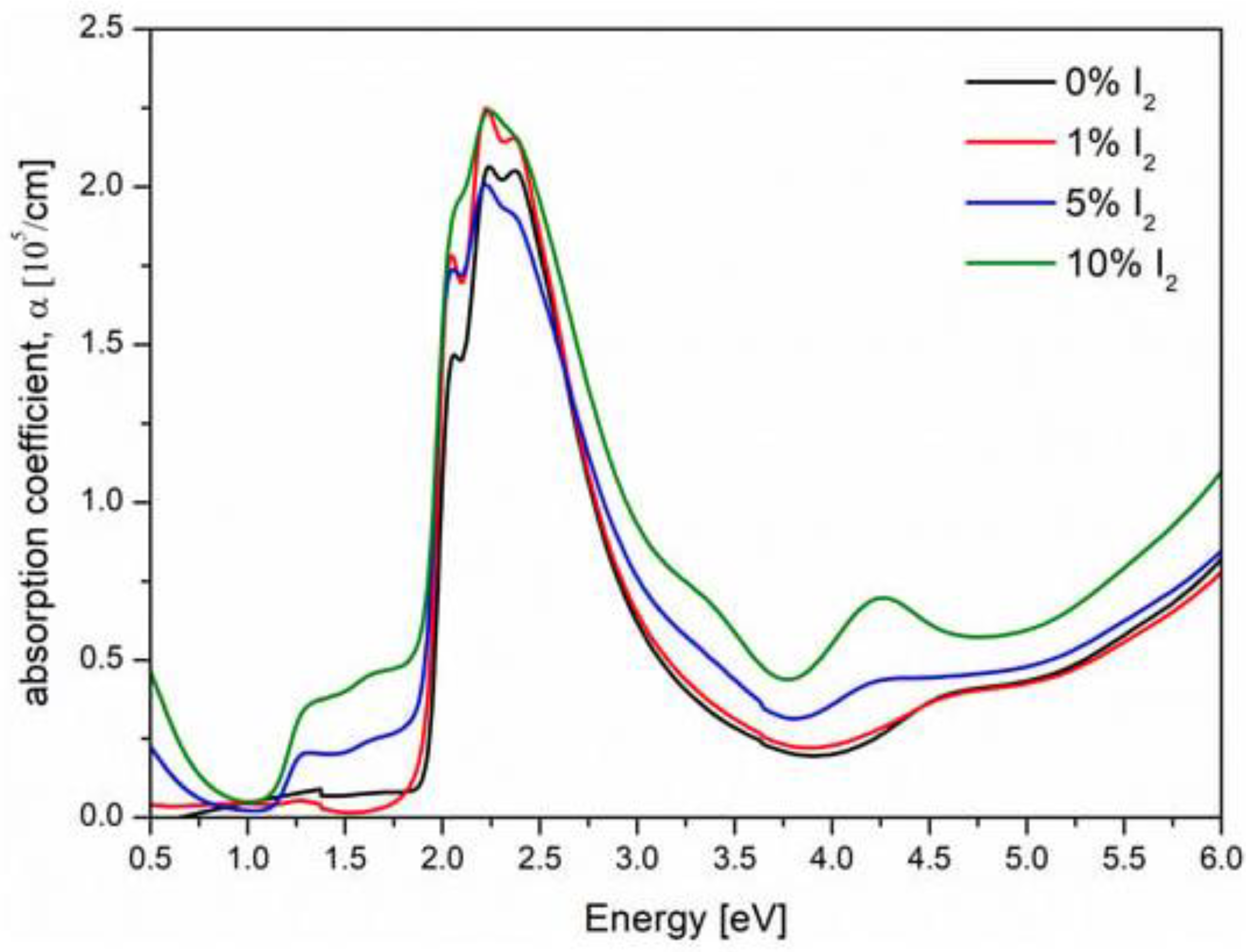
3. Results and Discussion

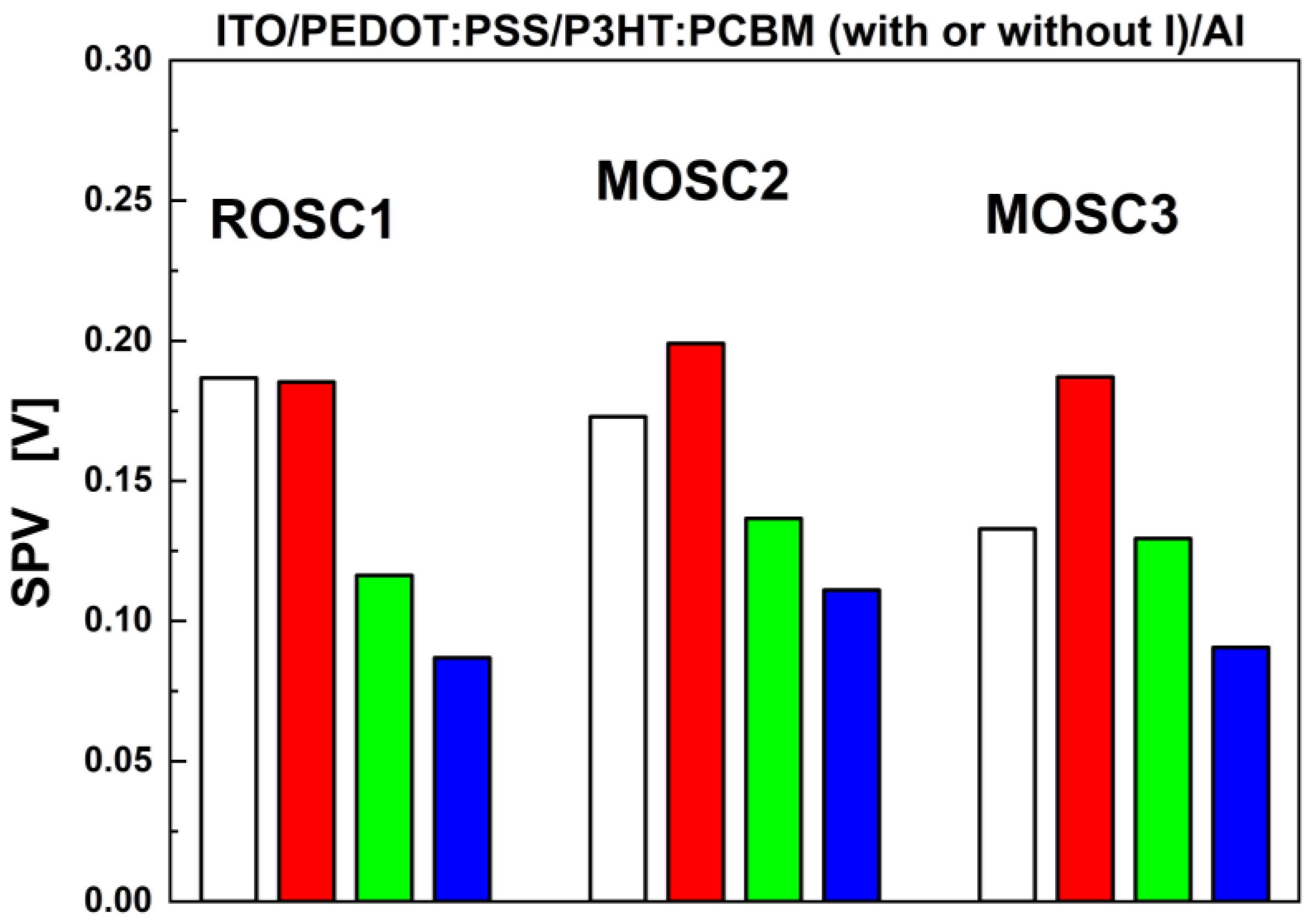
3.1. Photoactive Kelvin Probe Force Microscopy (p–KPFM)

The topography and surface potential images are presented as complementary maps in the Supplementary Information section, allowing the presence of topographical features and their impact on the surface potential distribution to be observed (see Figure S1).
As the samples were investigated in terms of their potential application in photovoltaic systems, the surface potential was analysed first. Figure 3 shows the SP values for each sample during illumination using various LEDs as described above, as well as in the dark. One should emphasize that there was some amount of red light (640 nm) present due to the laser beam-based scanning probe deflection detection system. One can see that there was a significant change in SP values when radiation was applied. Additionally, we observed that the abovementioned small dose of radiation delivered by the laser-based deflection system very likely had no significant impact on the samples, as the response obtained for red light exposure differed significantly from the response acquired in dark conditions. The response intensity (SP change) appeared in the following order: white, red, green and blue light. Based on that graph, one can tell that the best absorption and exciton generation were obtained for white light for all samples (ROSC1, MOSC 2-3) and for the red-light wavelength (see Figure 3). When the optical wavelength was shorter, the reaction of the material was smaller. One can also conclude that for white light, the red component was the most significant, yet in regard to this component, the largest differences between materials appeared.
The p-KPFM measurements also allowed us to estimate the surface photovoltage (SPV) [39] parameter at the micro- and nanoscale as a difference between the surface potential in the dark and under illumination (see Figure 4). It was also assumed that the response of the studied samples to white light was the same as or more intense than that to red, green or blue light. However, for the samples doped with iodine versus the reference sample (ROSC1), a decrease in the difference between SP in the dark and under the illumination of white light was observed.
The phenomenon of the more intense response of the studied samples with and without iodine doping to red light occurred because this particular wavelength was close to or even in the optical band gap of the P3HT donor polymer. Moreover, in the bulk heterojunction devices, an absorption distribution of a specific wavelength of light as a function of the active layer thickness and architecture of organic solar cells has been observed [40,41,42]. Taking into account that the studied organic solar half-cells were standard architecture devices (without a top electrode, ITO/PEDOT:PSS/active layer), the absorption distribution of light wavelength across the sample could be similar or even the same as that reported in the article by [40].
This leads to the conclusion that with the thickness of the active/organic layers between 80 nm and 110 nm, the most intense response observed in p-KPFM experiments is towards the red wavelength versus the dark measurements. Furthermore, regarding the results obtained from p-KPFM and the absorption coefficient published in our previous article [37], it is possible to notice that the absorption of blue and green light must be more intensive than that of red light (see also Figure 5). Nevertheless, the highest SPV values were observed for light from the red range wavelength, and such a phenomenon can be expected for the organic active layer doped with iodine. The incorporation of iodine ions into the mixture of polythiophene polymer with fullerene derivatives resulted in the better phase separation of P3HT and PCBM, a redshift of the absorption edge [43] and additional acceptor states in the energy band gap [44]. However, it is necessary to also take into account the fact that the surface photovoltage at different light wavelengths can have a significant influence on the “work function” of the active layer and, as a consequence, result in the modification of the HOMO and LUMO energy bands of organic materials with a metallic electrode that collects electrical charges. Further research is needed to better understand the interaction of different wavelengths of light with BHJ organic solar cells to determine the most effective charge recovery procedures for indoor applications.
In addition, the SP distribution was verified to check if the previously mentioned SP level differences were clearly above the distribution range. Typically, the SP variation was below 7 mV, which was much less than the observed SP level changes for different radiation wavelengths (see Figure S2 in the Supplementary Information). Only in three cases could one observe increased variation ranges, reaching a level of 21 mV. The topography analysis allowed us to find the correlation between unwanted features and the SP increased change range. One should emphasize that despite the selection of the analysed region, the influence of some unwanted long-range forces was observed. However, those ranges were still much below the SP value differences shown in Figure S2. Moreover, the morphological properties of the investigated films could have an impact on their surface and light interactions, which means that a certain roughness may improve the light absorption or increase the reflection factor. However, the analysis showed that regarding parameters such as Sq (root mean square deviation), Sku (kurtosis), Ssk (skewness), and Sdq (root mean square gradient), their obtained values showed relatively small differences (see Table S1 in the Supplementary Information) compared with those reported in other works [39,45,46,47].
Therefore, we assumed that the impacts of those parameters could be neglected and the only phenomena we considered to be responsible for the SP changes were the material electrical properties. The acquired data suggested the direction of future research, where certain materials should be implemented in a complete photovoltaic module and tested using standard investigation methods. Moreover, to identify the influences of electrical parameters on the efficiency of macroscale photovoltaic devices at the micro- and nanoscale, it is necessary to conduct a more detailed p-KPFM investigation. Issues that must be explored for a better understanding of the charge transport of and influence of dopants on the organic solar cell efficiency are related to the surface potential and influence of surface photovoltage [48,49,50] on the work function [49] of the organic active layer built into the architecture of solar cells.

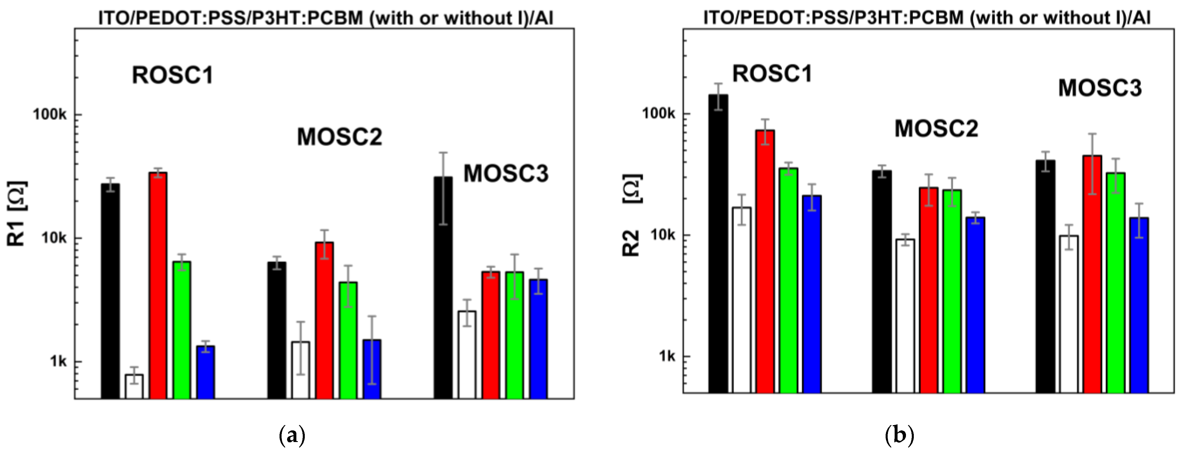
3.2. Photoactive Impedance Spectroscopy Experiments and Equivalent Electrical Circuit

One of the methods that allowed us to investigate the described charge transfer phenomena in solar cells with an active layer based on a mixture of donor polymers and acceptor materials was the impedance spectroscopy method [25,26,27,28,29,35,36,51,52,53,54,55,56]. Photoactive impedance spectroscopy (p-IS) experiments on the reference sample (ITO/PEDOT:PSS/P3HT:PCBM/Al) and photovoltaic devices with an active layer modified by adding iodine were conducted in this paper. p-IS measurements were carried out in the dark and under different ranges of wavelengths (under white, red, green and blue light, WRGB) for all samples at the macroscale. After analysis of the obtained data from p-IS for ROSC1, MOSC2, and MOSC3 third-generation photovoltaic devices, we decided to implement a series electric equivalent circuit to fit the obtained data and estimate the diffusion times of electrons and electron-hole recombination lifetimes. The results from the applied p-IS experimental approach are described and discussed below in relation to the photovoltaic results from our previous work [37].
The commonly used equivalent circuit for organic BHJ OS cells is shown in Figure 6 [51,54,56]. Its components are directly related to the measured impedance spectrum shown in the complex plane. Such a spectrum usually forms two semicircles, one recorded at lower frequencies and another at higher frequencies. Each semicircle is modelled with each parallel Rm-CPEm circuit. It is possible to evaluate the time constant of such a circuit:
τ m = R m T m 1 P m
where R m is the resistance and T m and P m are the parameters of CPEm.
According to Perrier et al. [54], the parameters of Rm and CPEm related to the high-frequency semicircle are related to the diffusion time of the electrons τ 1 , while the low-frequency semicircle is related to the effective lifetime of carriers related to electron-hole recombination τ 2 . An additional parameter R s is related to any series resistance in the cell and measurement setup, resulting in an impedance spectrum that shifts along the real axis. In Table S2 (see Supplementary Information), average parameters such as R s , R 1 , CPE1, R 2 , CPE2, τ 1 and τ 2 , obtained from the fitting procedure for the series equivalent circuit of impedance spectra for pixels of ROSC1, MOSC2 and MOSC3 samples (see Figures S3–S5), are presented. Applying the approach proposed by the authors of article [54], changes in the average values of resistances R 1 and R 2 were calculated and are shown in Figure 7, which allowed us to estimate the time constant associated with electron diffusion (τ1) and the recombination of electron-hole pairs (τ2) (see Figure 8). Moreover, by analysing the presented changes in resistances related to charge diffusion and recombination, it was deduced that the mentioned parameters were a function of both iodine doping and the type of illumination source used.
By analysing the standard deviation of the arithmetic mean and the estimated average values presented in Figure 7, it is possible to notice that the incorporation of dopant in the form of iodine into the active layer of the BHJ OSC (MOSC2, MOSC3) caused a decrease in the resistances R 1 and R 2 compared to the parameters of the reference sample (ROSC1) measured under dark conditions. This kind of electrical resistance behaviour, which consequently led to improved charge transport, was related to the influence of iodine on the structure of the active layer of the BHJ OSC devices, which resulted in improvements in the phase separation between P3HT and PCBM [43] and the P3HT crystallinity [37,57].
For light wavelengths in the red range, the resistance parameters of the tested BHJ OSC devices were very close to the values obtained from experiments performed without illumination. Taking into consideration the optical properties of the P3HT:PCBM blend, we concluded that light wavelengths in the red range spectrum were the least used for electrical charge generation in the BHJ OSC, which was expected because of the absorption distribution of light as a function of the active layer thickness [40,41,42]. To improve the impact of red light on the generation of electrical charges, the incorporation of dopants into the active layer or into the architecture of OSC has been proposed [43,44]. This approach can improve the harvesting of long-wavelength artificial red light located inside enclosed spaces.
When BHJ OSC devices were illuminated with blue light, the characteristics of resistances R 1 and R 2 were the same as those in experiments performed with white light. This kind of behaviour was expected because commercially available solid-state white light sources are built based on a blue diode with an appropriately selected luminophore. In turn, taking into account the mean values and fluctuations of the standard deviation of the resistances R 1 and R 2 of the considered photovoltaic devices (ROSC1, MOSC2, MOSC3) illuminated by green light, it was observed that the resistance values slightly changed with the doping of the active layer with iodine. The observed phenomenon was closely related to the fact that the green wavelength was most effectively used to generate electrical charges, and the reason for this was related to the optical properties of the P3HT polymer (see Figure 5, wherein the highest absorption coefficient value is for green light) and P3HT:PCBM blend (see Figure 6, from article [37]). All parameters estimated from p-IS for dark, white, red, green and blue artificial light sources related to nonmodified and modified standard bulk heterojunction organic solar cells are shown in Table S2 (see Supplementary Information).
Figure 8 shows the results of the estimation of relaxation times related to the electron diffusion (τ1) and recombination of electron-hole pairs (τ2) for doped and non-doped BHJ OSCs with iodine. In the case of p-IS measurements conducted in the dark and under green light, the relaxation times of charges related to τ1 and τ2 were maintained in the same way as the resistance described before R1 and R2, respectively (see Figure 7 and Figure 8 for comparison). Interesting phenomena occurred in the case of the illumination of BHJ OSC devices with white and blue light. An increase in electron diffusion times was observed for samples with iodine doping (MOSC2, MOSC3) compared to those of the reference sample (ROSC1). On the other hand, from p-IS experiments conducted under the illumination of red light, a decrease in τ1 parameters was observed for MOSC2 and MOSC3 devices compared to those of ROSC1 (see Figure 8).
The increase in τ 1 for doped samples illuminated by white and blue light was correlated with the thickness of the organic layer of the measured photovoltaic cells (see Table 1 and Figure 9), which was expected in the case of lengthening the diffusion path of the electrical charges.
It could be inferred that such an effect is undesirable. However, the decrease in the τ 2 parameter of doped devices relative to that of the reference sample under white and blue illumination should also be taken into account. Taking into account the dynamics of changes in the relaxation times τ 1 and τ 2 for samples illuminated under the entire visible spectrum and only with light from the blue range, it could be confidently concluded that the influence of the admixture in the active layer positively affected the operation of the BHJ OSC (see Figure 8, Table S2).
A correlation between the p-IS test results from this article and previously published photovoltaic measurements listed in Table 2 in [37] was noted, albeit only for devices illuminated with white light. The electron diffusion time increased with the thickness of the organic layer and iodine content, and the recombination time of electron-hole pairs decreased, which resulted in a reduction in the open-circuit voltage from 465.2 mV to 394.2 mV and 405.1 mV, and an increase in the short-circuit current density from 9.94 mA/cm2 to 12.95 mA/cm2 and 14.18 mA/cm2 for the ROSC1, MOSC2 and MOSC3 samples, respectively [37].
One of the most interesting p-IS experiments was carried out when photovoltaic devices were illuminated with red light. The doping of a composite material based on a donor polymer from the polythiophene family and the acceptor material PCBM with iodine increased the crystallinity of P3HT and thickened the organic layer [37,57], improved the phase separation between P3HT and PCBM [37,43,57], increased the Urbach energy after adding an admixture to the donor polymer [37], and shifted the absorption spectrum of the composite material towards longer wavelengths [43,44]. Moreover, an increasing Urbach energy of polymers and copolymers from the polythiophene family could cause an increase in the recombination rate phenomena of electrical charges in single-junction organic solar cells (SJ OSC) [58]. By analysing the p-IS results for wavelengths of light in the red range, a decrease in electron diffusion time was observed, which contrasted with the measurements for white and blue light illuminators. This discrepancy could be explained by the appearance of acceptor states in the energy gap and by a shifting of the entire polymer absorption spectrum towards red wavelengths. This would indicate that the p-IS measurement method could be used to identify the acceptor states in the energy gap in studies conducted under red light illumination conditions. In addition, p-IS experiments, carried out by exciting an operating organic photovoltaic device with a wavelength of approximately 660 nm, would allow the correlation between the Urbach energy value and electrical parameters of third-generation solar cells to be determined [58].

4. Conclusions

In conclusion, this paper describes the results of photoactive electrical measurements conducted using atomic force microscopy and impedance spectroscopy techniques. During the studies, bulk heterojunction organic half-cells and cells based on the P3HT:PCBM active layer were measured under working conditions. The influence of iodine p-type doping on the obtained electrical parameters at the macro- and nanoscale was considered. The use of different illumination sources to generate electrical charges in photovoltaic devices made it possible to estimate the effect of doping on the surface potential and demonstrate that the photovoltage obtained at the microscale depends on the light sources used and the doping level of an active organic layer. In the photoactive impedance spectroscopy studies, the decreasing diffusion time of electrons and electron-hole recombination lifetime were observed as a function of the doping level and thickness of organic layers.
It was observed that the nature of the changes in surface photovoltage estimated for organic half-cells under white light at 186.8 mV, 172.9 mV and 132.9 mV was similar to that of the changes in the fill factor (FF) of organic solar cells presented in our previous work [37], which was found to be 0.48, 0.46 and 0.44 for OSCs that were non-doped and doped with 5% and 10% iodine, respectively.
On the other hand, taking into consideration the behaviour of the relaxation times associated with the diffusion and recombination of electrical charges, described above, a correlation between the power conversion efficiency (PCE) of the non-doped and iodine-doped BHJ organic solar cells (5%, 10%) was observed with high probability. The values of PCE were published in reference [37] and were approximately 2.24%, 2.41%, and 2.61%, respectively.
Furthermore, the p-KPFM and p-IS measurement techniques could be applicable for the qualitative detection of additional acceptor states that occur in the optical energy gap of polymeric materials from the polythiophene family doped with acceptors and iodine ions.

Supplementary Materials

The following supporting information can be downloaded at: https://www.mdpi.com/article/10.3390/en16124741/s1, Figure S1: Topography (top, AFM) and surface potential (below, p-KPFM) of working half-cell photovoltaic devices based on an absorber P3HT:PCBM without (ROSC1) and with (MOSC2 and MOSC3) iodine doping; Figure S2: Values of the surface potential variation level obtained from p-KPFM of working half-cell photovoltaic devices in the dark and under different light sources; Figure S3. Measured (dots) and fitted (line) impedance spectra for 6 pixels (in rows) in ROSC1 sample measured in darkness and illumination. Figure S4. Measured (dots) and fitted (line) impedance spectra for 6 pixels (in rows) in MOSC2 sample measured in darkness and illumination. Figure S5. Measured (dots) and fitted (line) impedance spectra for 6 pixels (in rows) in MOSC3 sample measured in darkness and illumination. Table S1: Morphological properties of investigated films. Sq (root mean square deviation), Sku (kurtosis), Ssk (skewness) and Sdq (root means square gradient) parameters for the measurements of the samples ROSC1, MOSC2, MOSC3; Table S2: Summary of the EEC (a) modelling results for samples ROSC1, MOSC2 and MOSC3 in dark and illuminated states. Shown are: R s —contacts and connections resistance, R 1 - C P E 1 —parameters of R-CPE circuit related to τ 1 —diffusion time of electrons, R 2 - C P E 2 —parameters of R-CPE circuit related to τ 2 —electron-hole recombination.

Author Contributions

Conceptualization, M.P.; methodology, M.P., A.S., T.P., E.G. and P.N.; validation, P.N., P.G. and B.J.; investigation, M.P., T.P. and E.G.; writing—original draft preparation, M.P.; writing—review and editing, M.P.; visualization, A.S.; supervision, M.P., B.J. and T.G. All authors have read and agreed to the published version of the manuscript.

Funding

This research received no external funding.

Data Availability Statement

The data presented in this study are available on request from the corresponding authors.

Conflicts of Interest

The authors declare no conflict of interest.

References

  1. Huang, J.; Ren, Z.; Zhang, Y.; Liu, K.; Zhang, H.; Tang, H.; Yan, C.; Zheng, Z.; Li, G. Stretchable ITO-Free Organic Solar Cells with Intrinsic Anti-Reflection Substrate for High-Efficiency Outdoor and Indoor Energy Harvesting. Adv. Funct. Mater. 2021, 31, 2010172. [Google Scholar] [CrossRef]
  2. Lechêne, B.P.; Cowell, M.; Pierre, A.; Evans, J.W.; Wright, P.K.; Arias, A.C. Organic solar cells and fully printed super-capacitors optimized for indoor light energy harvesting. Nano Energy 2016, 26, 631–640. [Google Scholar] [CrossRef] [Green Version]
  3. Park, H.J.; Xu, T.; Lee, J.Y.; Ledbetter, A.; Guo, L.J. Photonic Color Filters Integrated with Organic Solar Cells for Energy Harvesting. ACS Nano 2011, 5, 7055–7060. [Google Scholar] [CrossRef] [PubMed]
  4. Mola, G.T.; Mthethwa, M.C.; Hamed, M.S.G.; Adedeji, M.A.; Mbuyise, X.G.; Kumar, A.; Sharma, G.; Zang, Y. Local surface plasmon resonance assisted energy harvesting in thin film organic solar cells. J. Alloys Compd. 2021, 856, 158172. [Google Scholar] [CrossRef]
  5. Agnihotri, P.; Sahu, S.; Tiwari, S. Recent Advances & Perspectives in Electron Transport Layer of Organic Solar Cells for Efficient Solar Energy Harvesting. In Proceedings of the International Conference on Energy, Communication, Data Analytics and Soft Computing, Chennai, India, 1–2 August 2017. [Google Scholar]
  6. Balasankar, A.; Arthiya, S.E.; Ramasundaram, S.; Sumathi, P.; Arokiyaraj, S.; Oh, T.; Aruchamy, K.; Sriram, G.; Kurkuri, M.D. Recent Advances in the Preparation and Performance of Porous Titanium-Based Anode Materials for Sodium-Ion Batteries. Energies 2022, 15, 9495. [Google Scholar] [CrossRef]
  7. Rajendhiran, R.; Atchudan, R.; Palanisamy, J.; Balasankar, A.; Oh, T.H.; Deivasigamani, V.; Ramasundaram, S. Prickly Pear Fruit Extract: Capping Agent for the Sol–Gel Synthesis of Discrete Titanium Dioxide Nanoparticles and Sensitizer for Dye-Sensitized Solar Cell. Coatings 2023, 13, 579. [Google Scholar] [CrossRef]
  8. Gnida, P.; Amin, M.F.; Pająk, A.K.; Jarząbek, B. Polymers in High-Efficiency Solar Cells: The Latest Reports. Polymers 2022, 14, 1946. [Google Scholar] [CrossRef]
  9. Caballero-Quintana, I.; Amargós-Reyes, O.; Maldonado, J.L.; Nicasio-Collazo, J.; Romero-Borja, D.; Barreiro-Arguelles, D.; Molnar, G.; Bousseksou, A. Scanning Probe Microscopy Analysis of Nonfullerene Organic Solar Cells. ACS Appl. Mater. Interfaces 2020, 12, 29520–29527. [Google Scholar] [CrossRef]
  10. Khatiwada, D.; Venkatesan, S.; Chen, Q.; Chen, J.; Adhikari, N.; Dubey, A.; Mitul, A.F.; Mohammed, L.; Qiao, Q. Improved performance by morphology control via fullerenes in PBDT-TBT-alkoBT based organic solar cells. J. Mater. Chem. A 2015, 3, 15307–15313. [Google Scholar] [CrossRef]
  11. Scherer, M.; Saive, R.; Daume, D.; Kröger, M.; Kowalsky, W. Sample preparation for scanning Kelvin probe microscopy studies on cross sections of organic solar cells. Appl. Phys. Lett. Adv. 2013, 3, 092134. [Google Scholar] [CrossRef] [Green Version]
  12. Chen, Q.; Mao, L.; Li, Y.; Kong, T.; Wu, N.; Ma, C.; Bai, S.; Jin, Y.; Wu, D.; Lu, W.; et al. Quantitative operando visualization of the energy band depth profile in solar cells. Nat. Commun. 2015, 6, 7745. [Google Scholar] [CrossRef]
  13. Saive, R.; Scherer, M.; Mueller, C.; Daume, D.; Schinke, J.; Kroeger, M.; Kowalsky, W. Imaging the Electric Potential within Organic Solar Cells. Adv. Funct. Mater. 2013, 23, 5854–5860. [Google Scholar] [CrossRef]
  14. Chen, Q.; Ye, F.; Lai, J.; Dai, P.; Lu, S.; Ma, C.; Zhao, Y.; Xie, Y.; Chen, L. Energy band alignment in operando inverted structure P3HT:PCBM organic solar cells. Nano Energy 2017, 40, 454–461. [Google Scholar] [CrossRef]
  15. Akaike, K. Distributions of Potential and Contact-Induced Charges in Conventional Organic Photovoltaics. Materials 2020, 13, 2411. [Google Scholar] [CrossRef]
  16. Kong, J.; Lee, J.; Jeong, Y.; Kim, M.; Kang, S.O.; Lee, K. Biased internal potential distributions in a bulk heterojunction organic solar cell incorporated with a TiOx interlayer. Appl. Phys. Lett. 2012, 100, 213305. [Google Scholar] [CrossRef]
  17. Glatzel, T.; Hoppe, H.; Sariciftci, N.S.; Lux-Steiner, M.C.; Komiyama, M. Kelvin Probe Force Microscopy Study of Conjugated Polymer/Fullerene Organic Solar Cells. Jpn. J. Appl. Phys. 2005, 44, 5370–5373. [Google Scholar] [CrossRef]
  18. Hoppe, H.; Glatzel, T.; Niggemann, M.; Hinsch, A.; Lux-Steiner, M.C.; Sariciftci, N.S. Kelvin Probe Force Microscopy Study on Conjugated Polymer/Fullerene Bulk Heterojunction Organic Solar Cells. Nano Lett. 2005, 5, 269–274. [Google Scholar] [CrossRef]
  19. Barsoukov, E.; Macdonald, J.R. Impedance Spectroscopy Theory, Experiment, and Applications; John Wiley & Sons, Inc., Publication: Hoboken, NJ, USA, 2005. [Google Scholar]
  20. Bisquert, J. Theory of the Impedance of Electron Diffusion and Recombination in a Thin layer. J. Phys. Chem. B 2002, 106, 325–333. [Google Scholar] [CrossRef]
  21. Bisquert, J. Interpretation of electron diffusion coefficient in organic and inorganic semiconductors with broad distributions of states. Phys. Chem. Chem. Phys. 2008, 10, 3175–3194. [Google Scholar] [CrossRef]
  22. Fabregat-Santiago, F.; Garcia-Belmonte, G.; Mora-Sero, I.; Bisquert, J. Characterization of nanostructured hybrid and organic solar cells by impedance spectroscopy. Phys. Chem. Chem. Phys. 2011, 13, 9083–9118. [Google Scholar] [CrossRef]
  23. Bisquert, J.; Mora-Sero, I.; Fabregat-Santiago, F. Diffusion–Recombination Impedance Model for Solar Cells with Disorder and Nonlinear Recombination. Chem. Electro. Chem. 2014, 1, 289–296. [Google Scholar] [CrossRef] [Green Version]
  24. Bisquert, J.; Bertoluzzi, L.; Mora-Sero, I.; Garcia-Belmonte, G. Theory of Impedance and Capacitance Spectroscopy of Solar Cells with Dielectric Relaxation, Drift-Diffusion Transport, and Recombination. J. Phys. Chem. C 2014, 118, 18983–18991. [Google Scholar] [CrossRef]
  25. Glatthaar, M.; Mingirulli, N.; Zimmermann, B.; Ziegler, T.; Kern, R.; Niggemann, M.; Hinsch, A.; Gombert, A. Impedance spectroscopy on organic bulk-heterojunction solar cells. Phys. Status Solidi 2005, 202, R125–R127. [Google Scholar] [CrossRef]
  26. Lu, L.; Luo, Z.; Xu, T.; Yu, L. Cooperative Plasmonic Effect of Ag and Au Nanoparticles on Enhancing Performance of Polymer Solar Cells. Nano Lett. 2013, 13, 59–64. [Google Scholar] [CrossRef]
  27. Glatthaar, M.; Riede, M.; Keegan, N.; Sylvester-Hvid, K.; Zimmermann, B.; Niggemann, M.; Hinsch, A.; Gombert, A. Efficiency limiting factors of organic bulk heterojunction solar cells identified by electrical impedance spectroscopy. Sol. Energy Mater. Sol. Cells 2007, 91, 390–393. [Google Scholar] [CrossRef]
  28. Garcia-Belmonte, G.; Boix, P.P.; Bisquert, J.; Sessolo, M.; Bolink, H. Simultaneous determination of carrier lifetime and electron density-of-states in P3HT:PCBM organic solar cells under illumination by impedance spectroscopy. Sol. Energy Mater. Sol. Cells 2010, 94, 366–375. [Google Scholar] [CrossRef]
  29. Garcia-Belmonte, G.; Munar, A.; Barea, E.M.; Bisquert, J.; Ugarte, I.; Pacios, R. Charge carrier mobility and lifetime of organic bulk heterojunctions analyzed by impedance spectroscopy. Org. Electron. 2008, 9, 847–851. [Google Scholar] [CrossRef]
  30. Kuwabara, T.; Kawahara, Y.; Yamaguchi, T.; Takahashi, K. Characterization of Inverted-Type Organic Solar Cells with a ZnO Layer as the Electron Collection Electrode by ac Impedance Spectroscopy. ACS Appl. Mater. Interfaces 2009, 1, 2107–2110. [Google Scholar] [CrossRef]
  31. Yo, J.; Chen, C.C.; Dou, L.; Murase, S.; Duan, H.S.; Hawks, S.A.; Xu, T.; Son, H.J.; Yu, L.; Li, G.; et al. Metal Oxide Nanoparticles as an Electron-Transport Layer in High-Performance and Stable Inverted Polymer Solar Cells. Adv. Mater. 2012, 24, 5267–5272. [Google Scholar] [CrossRef]
  32. Hau, S.K.; Yip, H.L.; Baek, N.S.; Zou, J.; O’Malley, K.; Jen, A.K.Y. Air-stable inverted flexible polymer solar cells using zinc oxide nanoparticles as an electron selective layer. Appl. Phys. Lett. 2008, 92, 253301. [Google Scholar] [CrossRef]
  33. Boix, P.P.; Ajuria, J.; Pacios, R.; Garcia-Belmonte, G. Carrier recombination losses in inverted polymer: Fullerene solar cells with ZnO holeblocking layer from transient photovoltage and impedance spectroscopy techniques. J. Appl. Phys. 2011, 109, 074514. [Google Scholar] [CrossRef]
  34. Zimmermann, B.; Wurfel, U.; Niggemann, M. Long term stability of efficient inverted P3HT:PCBM solar cells. Sol. Energy Mater. Sol. Cells 2009, 93, 491–496. [Google Scholar] [CrossRef]
  35. Iwan, A.; Palewicz, M.; Chuchmała, A.; Gorecki, L.; Sikora, A.; Mazurek, B.; Pasciak, G. Opto(electrical) properties of new aromatic polyazomethines with fluorene moieties in the main chain for polymeric photovoltaic devices. Synth. Met. 2012, 162, 143–153. [Google Scholar] [CrossRef]
  36. Iwan, A.; Palewicz, M.; Chuchmała, A.; Sikora, A.; Gorecki, L.; Sek, D. Opto(electrical) properties of triphenylamine-based polyazomethine and its blend with [6,6]-phenyl C61 butyric acid methyl ester. High Perform. Polym. 2013, 25, 832–842. [Google Scholar] [CrossRef]
  37. Jarząbek, B.; Nitschke, P.; Godzierz, M.; Palewicz, M.; Piasecki, T.; Gotszalk, T.P. Thermo-Optical and Structural Studies of Iodine-Doped Polymer: Fullerene Blend Films, Used in Photovoltaic Structures. Polymers 2022, 14, 858. [Google Scholar] [CrossRef]
  38. Nečas, D.; Klapetek, P. Gwyddion: An open-source software for SPM data analysis. Cent. Eur. J. Phys. 2012, 10, 181–188. [Google Scholar] [CrossRef]
  39. Iwan, A.; Sikora, A.; Hamplová, V.; Bubnov, A. AFM study of advanced composite materials for organic photovoltaic cells with active layer based on P3HT:PCBM and chiral photosensitive liquid crystalline dopants. Liq. Cryst. 2015, 42, 964–972. [Google Scholar] [CrossRef]
  40. Basta, M.; Dusza, M.; Palewicz, M.; Nawrot, U.; Granek, F. Method to analyze the ability of bulk heterojunctions of organic and hybrid solar cells to dissociate photogenerated excitons and collect free carriers. J. Appl. Phys. 2014, 115, 174504. [Google Scholar] [CrossRef]
  41. Feng, X.; Wang, Y.; Xiao, T.; Shen, Z.; Ren, Y.; Lu, G.; Bu, L. In Situ Measuring Film-Depth-Dependent Light Absorption Spectra for Organic Photovoltaics. Front. Chem. 2020, 8, 211. [Google Scholar] [CrossRef]
  42. Yang, C.; Zhao, C.; Sun, Y.; Li, Q.; Islam, M.R.; Liu, K.; Wang, Z.; Qu, S.; Wang, Z. Optical management in organic photovoltaic devices. Carbon Energy 2021, 3, 4–23. [Google Scholar] [CrossRef]
  43. Zhuo, Z.; Zhang, F.; Wang, J.; Wang, J.; Xu, X.; Xu, Z.; Wang, Y.; Tang, W. Efficiency improvement of polymer solar cells by iodine doping. Solid-State Electron. 2011, 63, 83–88. [Google Scholar] [CrossRef]
  44. Tian, P.; Tang, L.; Xiang, J.; Sun, Z.; Ji, R.; Lai, S.K.; Lau, S.P.; Kong, J.; Zhao, J.; Yang, C.; et al. Solution processable high-performance infrared organic photodetector by iodine doping. RSC Adv. 2016, 6, 45166–45171. [Google Scholar] [CrossRef]
  45. Bubnov, A.; Iwan, A.; Cigl, M.; Boharewicz, B.; Tazbir, I.; Wójcik, K.; Sikora, A.; Hamplova, V. Photosensitive self-assembling materials as functional dopants for organic photovoltaic cells. RSC Adv. 2016, 6, 11577–11590. [Google Scholar] [CrossRef]
  46. Iwan, A.; Boharewicz, B.; Tazbir, I.; Sikora, A.; Maliński, M.; Chrobak, Ł.; Mad, W. Laser Beam Induced Current Technique of Polymer Solar Cells Based on New Poly (Azomethine) or Poly (3-Hexylthiophene). Chem. Sci. Rev. Lett. 2015, 4, 597–607. [Google Scholar]
  47. Iwan, A.; Boharewicz, B.; Parafiniuk, K.; Tazbir, I.; Gorecki, L.; Sikora, A.; Filapek, M.; Schab-Balcerzak, E. New air-stable aromatic polyazomethines with triphenylamine or phenylenevinylene moieties towards photovoltaic application. Synth. Met. 2014, 195, 341–349. [Google Scholar] [CrossRef]
  48. Lee, S.J.; Kim, H.P.; bin Mohd Yusoff, A.R.; Jang, J. Understanding the role of organic polar solvent induced nanoscale morphology and electrical evolutions of P3HT:PCBM composite film. Org. Electron. 2015, 25, 50–56. [Google Scholar] [CrossRef]
  49. Spadafora, E.J.; Demadrille, R.; Ratier, B.; Grevin, B. Imaging the Carrier Photogeneration in Nanoscale Phase Segregated Organic Heterojunctions by Kelvin Probe Force Microscopy. Am. Chem. Soc. Nano Lett. 2010, 10, 3337–3342. [Google Scholar] [CrossRef]
  50. Grévin, B.; Bardagot, O.; Demadrille, R. Implementation of data-cube pump–probe KPFM on organic solar cells. Beilstein J. Nanotechnol. 2020, 11, 323–337. [Google Scholar] [CrossRef] [Green Version]
  51. Romero, B.; del Pozo, G.; Arredondo, B.; Reinhardt, J.P.; Sessler, M.; Wurfel, U. Circuital Model Validation for S-Shaped Organic Solar Cells by Means of Impedance Spectroscopy. IEEE J. Photovolt. 2015, 5, 234–237. [Google Scholar] [CrossRef]
  52. Arredondo, B.; Romero, B.; Del Pozo, G.; Sessler, M.; Veit, C.; Würfel, U. Impedance spectroscopy analysis of small molecule solution processed organic solar cell. Sol. Energy Mater. Sol. Cells 2014, 128, 351–356. [Google Scholar] [CrossRef]
  53. Knipper, M.; Parisi, J.; Coakley, K.; Waldauf, C.; Brabec, C.J.; Dyakonov, V. Impedance Spectroscopy on Polymer-Fullerene Solar Cells. Z. Naturforsch. 2007, 62, 490–494. [Google Scholar] [CrossRef]
  54. Perrier, G.; de Bettignies, R.; Berson, S.; Lemaître, N.; Guillerez, S. Impedance spectrometry of optimized standard and inverted P3HT-PCBM organic solar cells. Sol. Energy Mater. Sol. Cells. 2012, 101, 210–216. [Google Scholar] [CrossRef]
  55. Mullenbach, T.K.; Zou, Y.; Holst, J.; Holmes, R.J. Interpreting impedance spectra of organic photovoltaic cells—Extracting charge transit and recombination rates. J. Appl. Phys. 2014, 116, 124513. [Google Scholar] [CrossRef]
  56. Grancharov, G.; Atanasova, M.D.; Kalinova, R.; Gergova, R.; Popkirov, G.; Dikov, C.; Sendova-Vassileva, M. Flexible Polymer–Organic Solar Cells Based on P3HT:PCBM Bulk Heterojunction Active Layer Constructed under Environmental Conditions. Molecules 2021, 26, 6890. [Google Scholar] [CrossRef]
  57. Jarząbek, B.; Nitschke, P.; Hajduk, B.; Domanski, M.; Bednarski, H. In situ thermo-optical studies of polymer:fullerene blend films. Polym. Test. 2020, 88, 106573. [Google Scholar] [CrossRef]
  58. Tian, S.; Huang, T.; Han, F.; Wang, F.; Tan, Z.; Bai, Y. Optimization of tail state Urbach energy enables efficient organic solar cells and perovskite/organic tandem solar cells. Org. Electron. 2023, 113, 106714. [Google Scholar] [CrossRef]
Figure 1. Chemical structures of organic materials used for BHJ OSC preparation.
Energies 16 04741 g001
Figure 2. Schematic diagrams of the organic solar cell and half-cell: p-KPFM (left) and p-IS (right) experiments (* active layer with or without iodine doping).
Energies 16 04741 g002
Figure 3. Values of the surface potential obtained from p-KPFM experiments on working half-cell photovoltaic devices in the dark and under different light sources (Measurements carried out in the dark (black colour) and under white, red, green and blue light. Colours of bars corresponds the used light sources).
Energies 16 04741 g003
Figure 4. Surface photovoltage values obtained from p-KPFM as a difference between the surface potential of working half-cell photovoltaic devices in the dark and under illumination (Measurements carried out in the dark (black colour) and under white, red, green and blue light. Colours of bars corresponds the used light sources).
Energies 16 04741 g004
Figure 5. Absorption coefficient spectra of P3HT layers doped with 0%, 1%, 5% and 10% iodine from reference [37]. Reprinted from Ref. [37].
Energies 16 04741 g005
Figure 6. Series equivalent circuit used for fitting p-IS experimental data obtained for the ROSC1, MOSC2 and MOSC3 samples.
Energies 16 04741 g006
Figure 7. Changes in R 1 (a) and R 2 (b) resistances obtained from an EEC model for the reference (ROSC1) and modified (MOSC2, MOSC3) samples (Measurements carried out in the dark (black colour) and under white, red, green and blue light. Colours of bars corresponds the used light sources).
Energies 16 04741 g007
Figure 8. Changes in relaxation time calculated from an EEC model in the dark and under different light sources (Measurements carried out in the dark (black colour) and under white, red, green and blue light. Colours of bars corresponds the used light sources.): τ 1 —diffusion time of electrons (a), τ 2 —electron-hole recombination lifetime (b) (according to a scientific study published by Perrier et al. [52]).
Energies 16 04741 g008
Figure 9. SEM micrograph of a cross-section of an OSC. The image was taken using an electron beam in immersion mode with a current of 96 pA and acceleration voltage of 2 kV, with the SEM stage tilted at 52 degrees.
Energies 16 04741 g009
Table 1. Average thicknesses of each layer of the ROSC1, MOSC2 and MOSC3 samples at different locations of the cross-sections observed by SEM.
Type of Layer/LayersROSC1MOSC2MOSC3
Aluminium electrode
1 Organic layers: x and y
ITO
120.06 nm122.37 nm119.11 nm
85.48 nm98.04 nm111.09 nm
111.74 nm115.76 nm110.31 nm
1 Due to the low imaging contrast between the individual organic layers, i.e., x (PEDOT:PSS) and y (active layer, P3HT:PCBM without and with I), their combined thicknesses are shown.
Disclaimer/Publisher’s Note: The statements, opinions and data contained in all publications are solely those of the individual author(s) and contributor(s) and not of MDPI and/or the editor(s). MDPI and/or the editor(s) disclaim responsibility for any injury to people or property resulting from any ideas, methods, instructions or products referred to in the content.

