
Partial Discharge-Originated Deterioration of Insulating Material Investigated by Surface-Resistance and Potential Mapping


Department of Electrical and Power Engineering, Faculty of Electrical Engineering, Automatics, Computer Science, and Biomedical Engineering, AGH University of Krakow, al. Mickiewicza 30, 30-059 Krakow, Poland
*
Author to whom correspondence should be addressed.
Energies 2023, 16(16), 5973; https://doi.org/10.3390/en16165973
Submission received: 10 June 2023
/
Revised: 17 July 2023
/
Accepted: 2 August 2023
/
Published: 14 August 2023
(This article belongs to the Special Issue Dielectric Insulation in Medium- and High-Voltage Power Equipment—Degradation and Failure Mechanism, Diagnostics, and Electrical Parameters Improvement)
Abstract
:The endurance of medium- and high-voltage electrical insulation is a key reliability element in a broad spectrum of applications that cover transmission and distribution levels, the transportation segment, the industrial environment, and power electronics-based energy-conversion systems. The high electric-field stress and high-frequency switching phenomena as well as the impact of environmental conditions lead to the occurrence of partial discharges (PD) and the subsequent deterioration of electrical insulation. Partial discharges usually occur inside solid insulation materials in tiny voids that may either be located adjacent to the electrodes or in the bulk of dielectric material. This effect refers to both AC and DC systems; however, AC voltage is usually much more intensive as compared to DC voltage. This paper describes a novel combined approach based on surface-resistance and potential mapping to reveal the effects of internal processes and the deterioration of insulating material due to the actions of partial discharges. To realize the research objective, the following two-step approach was proposed. Multi-point resistance mapping enables us to identify the spots of discharge channels, manifesting a-few-orders-of-magnitude-lower surface resistance as compared to untreated areas. In addition, surface-potential mapping that was stimulated by corona-charge deposition reflects quasi-equipotential clusters and the related polarity-dependent dynamics of charge decay. A high spatial and temporal resolution allows for the precise mapping and tracing of decay patterns. Experiments were carried out on polyethylene (PE) and Nomex specimens that contained embedded voids. During PD events, the effective discharge areas are identified along with the memory effects that originate from the accumulation of surface charges. Long-term aging processes may drive the formation of channels that are initiated from the deteriorated micro clusters, in turn, penetrating the bulk isolation. The presented methodology and experimental results extend the insight into PD mechanisms and internal surface processes.
1. Introduction
The endurance of medium- and high-voltage (HV) electrical insulation is a key reliability element in a broad spectrum of applications that cover transmission and distributions levels, the transportation segment, the industrial environment, and power electronics-based energy-conversion systems [1,2,3,4,5,6]. The high electric field stress and high-frequency switching phenomena as well as environmental impacts such as temperature, humidity, or mechanical stresses lead to the occurrence of partial discharges (PD) and the subsequent deterioration of electrical insulation. This stimulates ongoing research on various characteristics of insulating materials, such as enhanced electrical endurance, high thermal conductivity, high energy storage density, extreme environmental resistance, and environmental friendliness [1,6]. Partial discharges usually occur inside solid insulation materials in tiny voids (gaseous inclusions) that may either be located adjacent to the electrodes or in the bulk of the dielectric material. This effect refers to both AC and DC systems; however, AC voltage is usually much more intensive as compared to DC voltage. The long-term penetration of PDs may lead to local surface degradation or treeing propagation, whose origins often occur at sharp edges where electric field amplification occurs. The deterioration of a void’s surface may result in radical surface-resistivity impairment—often by a few orders of magnitude; this creates local clusters that can even act as equipotential sheets. Such a conductivity non-homogeneity may thus impose a space-charge accumulation. This effect has an important role in HVDC (High Voltage Direct Current) insulation systems—especially related to power cables (considering their long-term endurance) [2]. A locally accumulated space charge may elevate operational stresses in HVDC polymeric cable systems—especially during polarity inversion [7]. The actions of partial discharges in gaseous inclusions result in changes in void surface conditions (for example, their conductivity, morphology, or roughness), which impacts the charge accumulation and transport effects [8,9,10,11,12,13]. Special attention is paid to investigations related to effective discharge and memory effects [10,14,15,16]. New insight was provided by mapping the discharge channels in the void creating an effective partial discharge area [17,18,19]. The modified surface conductivity of void walls impacts the decay time of deposited charges during consecutive PDs (thus, inception conditions in the long run) [20,21,22,23].
In this paper, partial discharge-originated deterioration was investigated by surface-resistance and surface potential-decay mapping. In this new approach, the effects of PD dynamics can be evaluated—especially revealing discharge channel clusters. The long-term exposure to partial discharges leads to variations in the discharge areas inside void walls, accelerating the clustering effect. In such a way, the evolution of so-called “effective discharge areas” may be observed [14,15,19,20], influencing the creation of discharge spots (thus, contributing to the stochastic character of the magnitude of partial discharges [21,22,23,24,25,26,27,28,29,30,31,32], which can be revealed during the acquisition by phase-resolved PD-pattern modulation [14,15,16,17,18,19]). These phenomena often contribute to memory effects [27,33,34,35]. The localization of surface clusters may even be impacted by the magnetic field, which influences the discharge trajectory [36,37]. The presented experiment was conducted on polyethylene (PE) and Nomex specimens that were subjected to accelerated deterioration stresses at 1 kHz. The samples took the form of a flat round gaseous inclusion with a diameter that was much larger than the thickness of an inclusion. The presented approach allowed for the localization of changes in a dielectric structure that was subjected to multi-channel PDs; these were identified through the detection of multi-point clusters with reduced surface resistances. Allocation to the clusters with different resistances by surface mapping reflected the energetic impact that is caused by partial discharges. The formation of the semiconducting surface inside voids may cause the creation of channels that penetrate toward the bulk in the next stage (e.g., the early stages of treeing). Such investigations aimed to better understand discharge mechanisms on the one hand and lead to the proper selection of the appropriate materials for HV insulation systems on the other. The novelty aspect of the paper refers also to the introduced measurement approach, which may be applied to the diagnostics of certain electrical power components, such as insulators, spacers, or power transformer insulating components during revisions. The compact version of the measurement rig will allow easy transportation to the inspection site, enabling easy diagnostics of the deterioration of the insulation materials.
The rest of this paper is organized as follows. The experimental methodology is presented in Section 2, followed by the specimen and measurement setup description in Section 3. The experimental results and discussion are in Section 4 and Section 5, respectively. Finally, the conclusion of this paper is drawn in Section 6.
2. Experimental Methodology
The intention of the performed experiments was to get inside the degradation processes that take place in sources of discharges that are embedded in dielectric insulation. The experimental methodology comprises five distinct phases, which are illustrated in Figure 1. The scope comprised the two-step approach proposed in this paper, related to surface-resistance and potential mapping. In the preparatory step, each specimen was cleaned and discharged while checking its condition with a measurement of the surface potential. The flat sample was formed on sheet layers of insulating material that contained an embedded round void. The void walls were explored during the experiments. A detailed description of the specimen’s geometry is presented in the following section. The investigations started with the accelerated degradation of the specimen after being subjected to a sinusoidal voltage of 18 kV and a frequency of 1 kHz for a predefined time period of 100 min. In this way, intensive partial discharges penetrated the void volume. In the second step, the specimens were opened in a clean environment, and both the upper and bottom walls were subjected to surface-resistance mapping that was performed automatically on a defined region. The investigated surface comprised the zone of the gaseous inclusion as well as an untreated external part for reference.
The third step was related to the DC corona charging of the void walls in the setup that is described in the next section. The polarity of the deposited charges was defined upfront. This phase was necessary to perform in the following fourth step the surface-potential mapping, including the time-decay observation along the marked cross-sections (fifth step). In this way, the partial discharge-deteriorated insulating material inside the void was analyzed by means of both surface-resistance testing and potential mapping.
3. Specimen and Measurement Setup
In this section, detailed descriptions of the specimens, setup, and measurement instrumentation are provided.
3.1. Specimens
The presented experiment was conducted on polyethylene (PE) and Nomex® (DuPont, Wilmington, NC, USA, Type 418 flexible paper with a rated temperature range of 220 °C and a sheet thickness of 120 μm) specimens that were subjected to an accelerated deterioration stress at 1 kHz. Both materials are extensively used in high-voltage applications; polyethylene is a basic material for the main insulation of polymeric high-voltage cables, while Nomex is applied in the transformer layer and ground insulation as well as the insulation of motor coil wraps and conductors (the latter’s calendared blend of mica and aramid provides increased voltage corona endurance). The investigated Nomex 418 contained a 50% share of mica lamellas. The aramid paper eliminated the main drawbacks of cellulose, i.e., reduced moisture absorption as well as increased resistance to high temperatures. The typical electrical properties for PE and Nomex 418 are presented in Table 1.
Specimens from both materials (format 100 × 100 mm) were designed according to the geometry that is shown in Figure 2; these contained flat round gaseous inclusions with a diameter of d = 38 mm, which is much larger than the thickness of an inclusion (a = 1 mm—d >> a). The main specimen insulation was composed of three layers (each 1 mm thick) with a punched void in the middle one. Two glass plates (1 mm thick each) were pressed on both sides of the samples to safeguard their mechanical stability. The investigated surfaces (the upper and bottom void walls) are marked in red in Figure 2. The surface-resistance and potential mapping was carried out on these layers after opening the specimen.
Both high-voltage and ground electrodes made of stainless steel (diameter—50 mm) ensured a uniform electric field distribution. The measurements were performed in insulating oil in order to prevent surface discharges on the specimen. The following environmental conditions were present during the experiments: a temperature of 24 °C, a humidity level of 31%, and an atmospheric pressure of 999 hPa.
3.2. Measurement Setup
The measurement setup elements that are described in this section refer to the consecutive stages in the experimental framework; i.e., accelerated deterioration of specimens with AC voltage, DC charge sprinkling in corona mode, and both surface-resistance and potential mapping.
3.2.1. Accelerated Specimen Degradation
The simultaneous accelerated degradation of both the PE and Nomex specimens was conducted with a sinusoidal voltage of 18 kV and a frequency of 1 kHz for a predefined time period of 100 min. The electrical exposure setup is shown in Figure 3. The high voltage was delivered from a Trek 20/20B amplifier (Advanced Energy, Denver, CO, USA), which was controlled by a SIGLENT function generator (Siglent, Shenzhen, China). The HV source was protected with a Z = 2 MΩ resistor. The level of the high voltage was measured by means of a Tektronix Probe (Tektronix, Beaverton, OR, USA, Model P6015A—depicted in Figure 3) represented by an R1 and R2 resistive divider, with an input impedance equal to 100 MΩ, providing an attenuation factor of 1:1000.
The presence of partial discharges was detected by a CT wideband current transformer that was terminated at 50 Ω and placed on the ground side and observed on an oscilloscope. The aging conditions were set based on the performed tests. The voltage was adjusted to the level above the partial discharge inception voltage. The higher frequency was ensuring the acceleration of the specimen deterioration. The duration of the test was set according to the visible aging effects.
3.2.2. DC Charge Sprinkling
The charge-sprinkling setup (shown in Figure 3b) was used to accumulate the charge of the defined polarity on the specimen surface. In corona mode, DC voltage that was equal to ±18 kV was applied to an HV needle electrode with a radius of 700 μm that was positioned at a distance h of 100 mm above the sample surface (with thickness dl located on the ground planar electrode). The relatively great distance between the needle tip and the specimen surface resulted in a quite-uniform charge deposition. The void region is marked in red in Figure 3b. The duration of the flash-sparkling process was 10 s. The voltage potential related to the charge density was measured by using the system that is described in the next section.
3.2.3. Surface-Resistance Mapping
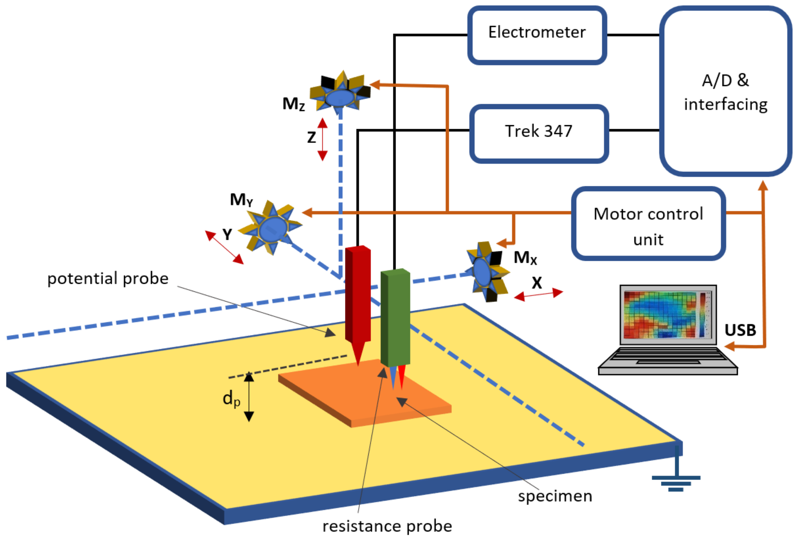
The measurements of the surface-resistance mapping on the void walls were performed in the setup that is presented in Figure 4. The multipoint method that was described in [18] was applied to visualize the potential distribution in the frame of the investigated region. The scanning was executed fully automatically along a programmed line-by-line pattern. The interelectrode distance of the probe was equal to 5 mm. The mobile micro two-electrode probe was automatically positioned along the x- and y-axes above the defined zone of investigation. The control along the z-axis ensured the proper pressure and contact between the measuring electrodes and the specimen surface. The probe was driven by three USB-controlled motors (Mx, My, and Mz), which positioned the resistance probe in three dimensions at defined coordinates in space. The measurement of the surface resistance was performed by an electrometer through a current measurement at an applied voltage of 1 kV. The results were sent to the computer via a USB interface. The mapping sequence was executed along the defined trajectory at defined grid points. The surface-resistance mapping was carried out in a matrix of 25 × 25 = 625 points, i.e., covering a region of 60 × 60 mm with a raster of 2.5 mm. Both the upper and lower void walls were investigated.
3.2.4. Surface-Potential Mapping
The measurements of the surface-potential mapping and decay-time estimation were performed in the setup that is presented in Figure 4. Based on this approach, the surface-charge density could also be calculated [38,39,40,41]. One side of the void wall specimen material was put on the grounded electrode. The mobile-readout probe was automatically positioned along the x- and y-axes above the selected region of investigation. The control along the z-axis allowed for the precise positioning of the probe above the specimen. The head that fixed the probe was driven by three USB-controlled motors (Mx, My, and Mz), which positioned the probe in three dimensions. The readout of the surface potential was carried out by means of an electrostatic voltmeter (Trek Model 347), which was directly connected to a 16-bit A/D converter and a computer-interfacing USB module. The potential measurement was based on a non-contacting field-nulling approach [38]. In the surface-potential mapping mode, the probe was positioned at a distance of dp = 1 mm above the specimen. The surface-potential mapping was carried out in a matrix of 25 × 25 = 625 points, i.e., covering a region of 60 × 60 mm with a raster of 2.5 mm. The probe-to-plane distance was 1 mm. The upper and lower sheets of the void specimen were investigated. For visualization in both the surface-resistance and surface-potential mapping cases, the interpolation of the surface color distribution was applied using the measurement values from the grid nodes. For the interpolation, a cubic convolution from Matlab (ver. R2022a) was used.
4. Results
The measurements were executed according to the methodology that was described in the previous section (distinguishing several stages). The experiments started with an accelerated deterioration of specimens at an AC voltage of 18 kV and a frequency of 1 kHz for 100 min. The experimental setup of the PD exposition phase was presented in Figure 3. The intensive action of the partial discharge inside the embedded void resulted in internal surface degradation. The individual channels on both the upper and lower inclusions’ voids were created. After a longer stressing time, these local spots formed bigger clusters that were characterized by lower surface resistance. The identification of these effects in both specimens is the subject of this paper and will be described in the following parts.
4.1. Surface-Resistance Mapping
One of the degradation-assessment methodologies that are presented in this paper is surface-resistance mapping. The applied instrumentation allowed for the automatic execution of the mapping of a defined region. The surface resistances of the untreated non-aged materials were higher than Rs > 1014 Ω in the case of PE and higher than Rs > 1012 Ω for Nomex. The surface-resistance mapping of the bottom side of the PE and Nomex specimens that was carried out on region (x, y) = (−30, 30; −30, 30) [mm] is shown in Figure 5. The void wall could be very well-distinguished from the untreated external zone. The deteriorated regions manifested two-orders-of-magnitude-lower resistance as compared to the non-aged parts; i.e., for PE, the value dropped from 3.1 × 10¹³ to 1011 Ω, and in the case of Nomex, it dropped from 1.6 × 10¹² to 1.6 × 10¹⁰ Ω. The region of the accelerated deterioration is well-marked in the 3D (Figure 5c,d) and cross-section views (Figure 5e,f). The resistance mapping reveals the creation of a quasi-equipotential zone (corresponding to the void diameter) on one side with a significantly increased level of surface conductivity. On the other hand, one can even observe the clusters and zones in that region that corresponded to the more- and less-intensive discharge channels.
4.2. Surface-Potential Mapping
In order to reveal the deteriorated clusters, the void walls were exposed to a charge deposition with a defined polarity in the corona mode in the setup that is shown in Figure 3b. Charge sprinkling at ±20 kV DC was conducted during a flash-exposition time of 10 s. Immediately after the charge deposition, the electrostatic-potential surface mapping was performed by using the instrumentation that is described in Section 3.2.4.
The surface-potential mapping on the void walls of the PE specimens (bottom sides) is shown in Figure 6a,b (3D view) for the negative polarity and Figure 6c,d (3D view) for the positive polarity of the accumulated charge. An analogic sequence of the surface-potential mapping on the void walls of the Nomex specimens is shown in Figure 7a for the negative and Figure 7b for the positive sprinkling. In both cases, the void regions were well-defined; the contours of the voids (with a diameter of 38 mm) are clearly visible in the patterns that are shown in Figure 6 and Figure 7. The course of the surface potential within the void wall zone in fact reflects the equipotential cluster, which was identified by the surface-resistance mapping as a region with significantly reduced surface resistance.
The potential measurements indicated the PD accumulated-charge zones, which were concentrated quasi-radially. Due to the intensive accelerated deterioration test (high-frequency and high-electric field stress), the spatial distribution of the PD filamentary channels became more and more uniform in their shapes. The mechanism of these effects also referred to the memory mechanism that was related to the individual PD events [12,21,27,35].
5. Discussion
The analysis of the partial discharge-originated degradation of insulating material that is presented in this paper was carried out jointly by two techniques: namely, surface-resistance mapping and surface-potential mapping. The former was performed directly after accelerated deterioration tests at 1 kH, while the latter was executed in the second step immediately after the DC charge deposition with a known polarity. There are mainly three physical mechanisms that are associated with surface-charge decay: namely, gas neutralization due to environmental exposition (incl. the impacts of humidity and temperature), surface conduction, and bulk transport [27,33,34]. All of these mechanisms may have been present in the experiment; however, they would have manifested different dynamics. Surface conduction may have especially been present in the deteriorated regions on the gaseous inclusion walls. In this way, even separate spots that exhibited elevated levels of surface conductivity may have formed joint clusters over time. Also, the void boundary that represented the strong electric field tangential component due to the charge non-homogeneity may have supported this effect. In turn, the bulk transport could have been characterized by charge injection (dependent on the mobility and density of the charge carriers), polarization, and intrinsic conduction [34]. In the case of the flat specimen geometry and neglecting the existence of a space charge in the material bulk, the surface potential could have been assumed to be proportional to the surface-charge density. The applied combination of the surface-resistance and potential mapping revealed the effects of partial discharge action on a dielectric surface in two domains in a quantitative way; one reflecting the degradation level, and the second revealing the dynamics of the charge neutralization and transport. The graphical visualization of the mapping effects on the surface of the deteriorated insulating material is illustrated in Figure 8. The shown symbolic grid layout density depends on the applied measurement conditions, and the resolution can be separately defined for the resistance and potential measurements. There is a tradeoff between the raster spatial resolution and the total scanning time. The boundary of the void is marked in the graph, indicating the upper and bottom walls as well as distinguishing the untreated and deteriorated areas.
The surface resistance-mapping results that were presented in the previous section (Figure 5) exhibit the PD channel-formation spots on the void walls with high resolution. The inclusion contour can be well-distinguished as well as the clusters inside the void that corresponded to the intensities of the PD at different spots. After extraction, the exact void areas for both specimens are shown in Figure 9.
In order to assess the degree of surface degradation, the following classification procedure was applied [19]. Threshold levels on the surface resistance were defined, which allowed us to reveal the regions, which dropped one, two, or more orders of magnitude from the reference untreated level. The corresponding areas were calculated according to the following formula:
where Thlow_i, Thhigh_i define the thresholds that specified the sub-regions. In particular, Thlow_i can be set to zero; in this way, the area with a resistance below the Thhigh_i value will be visualized. The percentage share Pi of this region with respect to the whole area of the void with diameter d yields the following:
According to the above procedure, the degradation degrees (expressed by Pi) for both the PE and Nomex specimens are shown in Table 2. The threshold levels in the case of PE showed a drop in surface resistance R by three orders of magnitude, whereas Nomex showed a drop of two orders. The surface-resistivity mapping for the PE specimen with the applied thresholding (going down order by order of magnitude) is presented in Figure 10.
The highest conductance (R < 1011) was attributed to 17% of the void area, while the majority was occupied by a cluster where R < 1012 (56.3%) and R < 1013 (98.9%). However, radically different patterns were revealed in these two cases. The centric and radial focus in the first case that reflected the high-intensity PDs can be noticed, whereas the latter one represents the discharges that occurred around the boundary of the outer gas inclusion. In the cases of the regions with the lowest resistance (R < 1011), the tiny hot spots are well-visible; these can be attributed to those places where the PDs had the greatest impacts.
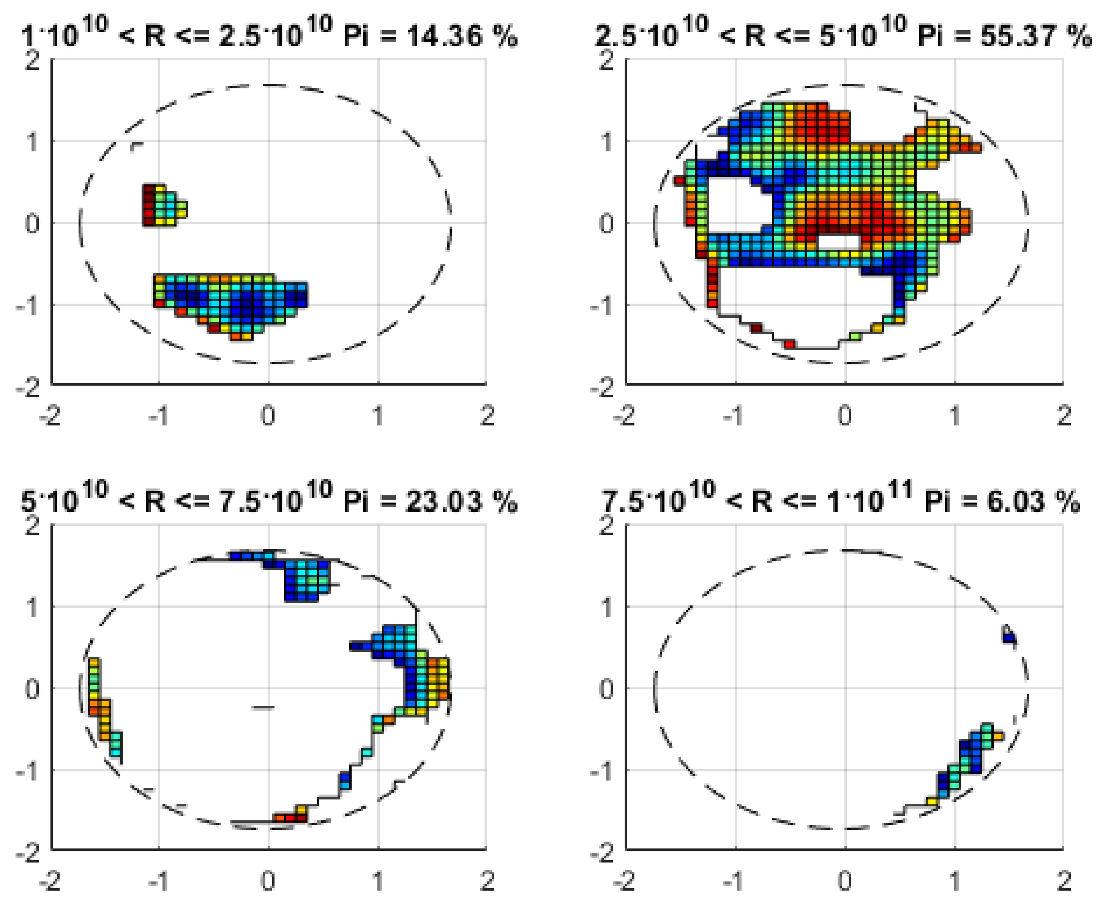
In the case of Nomex (Figure 11), individual thresholding was applied since the span was smaller.
The highest conductance (R < 2.5 × 10¹⁰) could be attributed to 14.4% of the void area, whereas the majority was occupied by clusters for those resistances that were within a range of 2.5 × 10¹⁰ < R < 5 × 10¹⁰ (Pi = 55.4%). This is represented by a rather strongly clustered pattern that was centrally located in the void. The spot was relatively big in this case, unlike the individual dots that could be observed in the PE case above (Figure 10). The strongest PD action could be observed when applying the threshold (R < 2.5 × 10¹⁰).
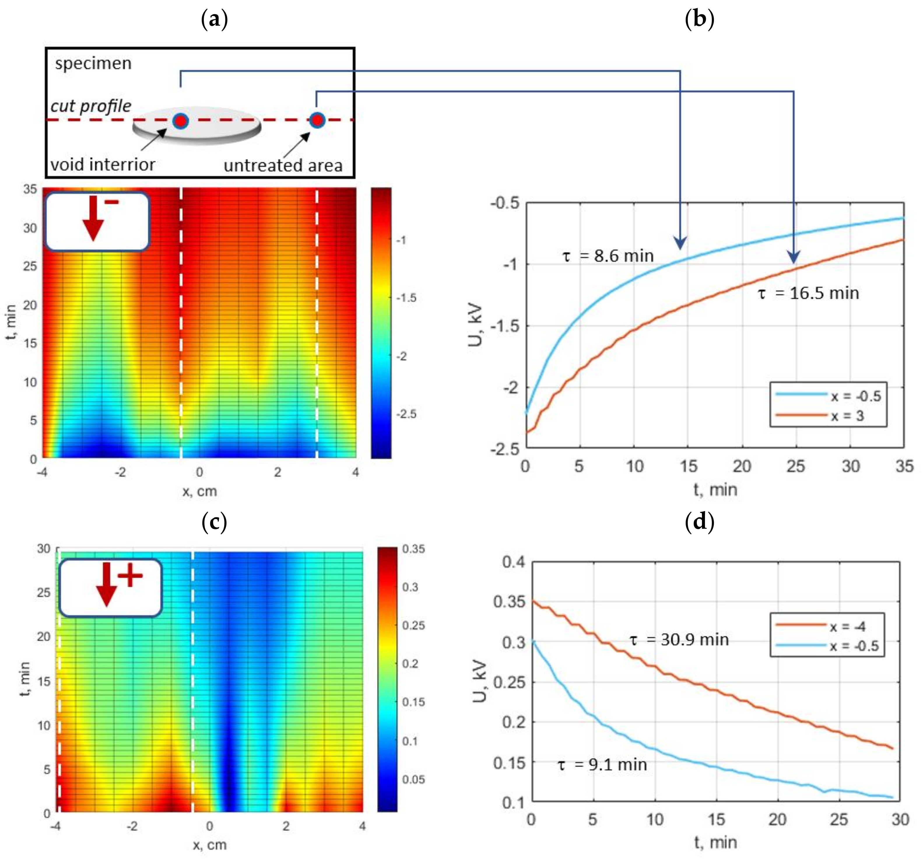
After the positive and negative charge depositions (shown in Figure 6 and Figure 7 for the PE and Nomex specimens, respectively), the surface potential-mapping results exhibited the boundaries of the equipotential areas. From this perspective, the void interior represented a quite uniform and clustered pattern, even though the individual sub-regions that were distinguished by the resistance mapping may have varied in the order of the magnitude of their surface-resistance values. To analyze the dynamics of the surface-potential decay, the measurements were performed along a cross-section of the inclusion (along the x-axis at y = 0), passing both the untreated region and alongside the void diameter. In all of the cases, the charge was deposited in corona mode at 20 kV over a short time period (10 s). The time evolutions that were acquired over 35 min for the Nomex sample (bottom side) are shown in Figure 12a,b (negative polarity) and Figure 12c,d (positive polarity). To reveal the decay-time constants, the cuts that are marked by the white dashed lines in Figure 12a,c are shown in the plot in Figure 12b,d. For the deposition of the negative charge, the blue line in the plot (Figure 12b) traveled through the middle of the void and had a decay time of τ = 8.6 min, whereas the brown line (representing the untreated region) yielded τ = 16.5 min.
In the case of the positively polarized Nomex specimen’s surface, a cross-section is shown in Figure 12c, and the corresponding cuts along the decay time are shown in Figure 12d. The blue line that is marked through the middle of the void had a decay time of τ = 9.1 min, whereas the brown line (representing the untreated region) yielded τ = 30.9 min. The polarity-dependent decay times were radically different for the non-aged region (and were much longer for the positive charging), whereas the potential-decay times inside the deteriorated void were quite similar for both polarities.
The presented approach revealed the non-homogenous deterioration of the void walls, which reflected the exact spots of strong PD penetration. In both cases (PE and Nomex), more-intensive PD action could be observed in the central and radial directions than at the inclusion’s external round and boundary zones. The long-term partial discharge exposure resulted in the transition of the effective discharge area. The presented approach may also be utilized in research on the various charge-decay mechanisms.
6. Conclusions
The goal of this paper was to describe a novel combined approach that was based on surface-resistance and potential mapping to reveal the effects of the internal processes and deterioration of insulating materials due to the actions of partial discharges. A dedicated measurement methodology was elaborated in order to properly address these measurements. The experiments were performed on flat PE and Nomex specimens that contained embedded voids. Multi-point resistance mapping allowed us to identify the spots of the discharge channels, which manifested a few orders of magnitude lower surface resistance as compared to the untreated areas. In addition, surface-potential mapping that was stimulated by corona-charge deposition reflected the quasi-equipotential clusters and related dynamics of the charge decay. The derived time evolution of the surface-potential mapping revealed quite similar decay times for the deteriorated void interior (negative charging of Nomex—τ = 8.6 min; positive charging—τ = 9.1 min); these reflected the corresponding drops in the surface resistance. The high spatial and temporal resolution allowed for the precise mapping and tracing of the decay patterns. During the PD events, the effective discharge areas were identified with the memory effects that originated from the accumulation of the surface charges. The experimental results showed the formation of clusters in the deteriorated area, which revealed a few orders of magnitude reduced surface resistance; the developed methodology allowed for the precise localization of these regions. The surface-potential mapping indicated those spots that represented the equipotential behavior and quantitatively showed the potential decay processes. The two measurement approaches that were presented reflected a quantitative correlation and correspondence between the untreated and aged regions (pinpointing subclusters in the latter case). It could be observed that the PD action resulted in a few orders of magnitude surface resistance drop in the deteriorated void areas. Furthermore, the potential mapping revealed the creation of equipotential clusters. The patterns of the clusters and the individual spots reflected the local PD intensities. It can be stated that the void walls were not homogenously stressed nor deteriorated, leading to the formation and transition of the effective discharge area within the aging time. The long-term aging processes may have driven the formation of channels that were initiated from the deteriorated micro clusters, in turn, penetrating the bulk isolation. The introduced measurement approach may be applied to the diagnostics of certain electrical power components, such as high-voltage insulators, GIS/GIL spacers, or power transformer insulating component during revisions. The compact version of the measurement rig will allow easy transportation to the inspection site. The follow up work will be two-fold, on one site will refer to the extensions of the measurement setup capabilities in terms of the further improvement of the sensitivity, probe design and measurement speed of the overall procedure, on the other side will focus on the theoretical foundations and interpretation of the obtained results. The presented methodology and experimental results extend the insight into PD mechanisms and internal surface processes.
Author Contributions
Conceptualization & methodology, M.F. and M.K.; formal analysis, M.F. and M.K. investigation and resources, M.F. and M.K.; data curation, M.F. and M.K.; writing—original draft preparation, M.F. and M.K.; visualization, M.F. and M.K.; supervision and project administration, M.F. and M.K. All authors have read and agreed to the published version of the manuscript.
Funding
This research received no external funding.
Data Availability Statement
Not applicable.
Conflicts of Interest
The authors declare no conflict of interest.
References
- Li, C.; Yang, Y.; Xu, G.; Zhou, Y.; Jia, M.; Zhong, S.; Gao, Y.; Park, C.; Liu, Q.; Wang, Y.; et al. Insulating materials for realising carbon neutrality: Opportunities, remaining issues and challenges. High Volt. 2022, 7, 610–632. [Google Scholar] [CrossRef]
- Mazzanti, G. Issues and Challenges for HVDC Extruded Cable Systems. Energies 2021, 14, 4504. [Google Scholar] [CrossRef]
- Rajashekara, K. Power Conversion Technologies for Automotive and Aircraft Systems. IEEE Electrif. Mag. 2014, 6, 50–60. [Google Scholar] [CrossRef]
- Rumi, A.; Lusuardi, L.; Cavallini, A.; Pastura, M.; Barater, D.; Nuzzo, S. Partial Discharges in Electrical Machines for the More Electrical Aircraft. Part III: Preventing Partial Discharges. IEEE Access 2021, 9, 30113–30123. [Google Scholar] [CrossRef]
- Fabiani, D.; Montanari, G.C.; Cavallini, A.; Mazzanti, G. Relation between Space Charge Accumulation and Partial Discharge Activity in Enameled Wires under PWM-like Voltage Waveforms. IEEE Trans. Dielectr. Electr. Insul. 2004, 11, 393–405. [Google Scholar] [CrossRef]
- Lebey, T.; Rumi, A.; Cavallini, A. Challenges for Electrical Insulation Systems in High Voltage Aviation Applications. IEEE Electr. Insul. Mag. 2022, 38, 5–11. [Google Scholar] [CrossRef]
- Mazzanti, G.; Chen, G.; Fothergill, J.; Fu, M.; Hozumi, N.; Lee, J.H.; Li, J.; Marzinotto, M.; Mauseth, F.; Morshuis, P.; et al. The insulation of HVDC extruded cable system joints. Part 1: Review of materials, design and testing procedures. IEEE Trans. Dielectr. Electr. Insul. 2019, 26, 964–972. [Google Scholar] [CrossRef]
- Tanaka, T. Internal partial discharge and material degradation. IEEE Trans. Dielectr. Electr. Insul. 1986, EI-21, 899–905. [Google Scholar] [CrossRef]
- McAllister, I.W. Decay of charge deposited on the wall of gaseous void. IEEE Trans. Electr. Insul. 1992, 27, 1202–1207. [Google Scholar] [CrossRef] [Green Version]
- Tanaka, T.; Uchiumi, M. Two kinds of decay time constants for interfacial space charge in polyethylene-laminated dielectrics. In Proceedings of the 1999 Annual Report Conference on Electrical Insulation and Dielectric Phenomena, Austin, TX, USA, 17–20 October 1999; pp. 472–475. [Google Scholar]
- Niemeyer, L. A generalized approach to partial discharge modeling. IEEE Trans. Dielectr. Electr. Insul. 1995, 2, 4. [Google Scholar] [CrossRef] [Green Version]
- Florkowski, M. Influence of Insulating Material Properties on Partial Discharges at DC Voltage. Energies 2020, 13, 4305. [Google Scholar] [CrossRef]
- Gutfleisch, F.; Niemeyer, L. Measurement and simulation of PD in epoxy voids. IEEE Trans. Dielectr. Electr. Insul. 1995, 2, 729–743. [Google Scholar] [CrossRef]
- Wu, K.; Suzuoki, Y. Effects of discharge area on PD patterns in voids. In Proceedings of the 1999 Annual Report Conference on Electrical Insulation and Dielectric Phenomena, Austin, TX, USA, 17–20 October 1999; pp. 227–230. [Google Scholar]
- Florkowska, B. Partial discharge measurements with computer aided system in polyethyleneterephthalate and polypropylene films. In Proceedings of the 8th International Symposium on High Voltage Engineering, Yokohama, Japan, 23–27 August 1993; pp. 41–44. [Google Scholar]
- Florkowski, M.; Florkowska, B.; Włodek, R. Investigations on post partial discharge charge decay in void using chopped sequence. IEEE Trans. Dielectr. Electr. Insul. 2017, 24, 3831–3838. [Google Scholar] [CrossRef]
- Wu, K.; Ijichi, T.; Kato, T.; Suzuoki, Y.; Komori, F.; Okamoto, T. Contribution of surface conductivity to the current forms of partial discharges in voids. IEEE Trans. Dielectr. Electr. Insul. 2005, 12, 1116–1124. [Google Scholar]
- Florkowski, M.; Florkowska, B.; Kuniewski, M.; Zydron, P. Mapping of discharge channels in void creating effective partial discharge area. IEEE Trans. Dielectr. Electr. Insul. 2018, 25, 2220–2228. [Google Scholar] [CrossRef]
- Florkowski, M.; Kuniewski, M. Correspondence Between Charge Accumulated in Voids by Partial Discharges and Mapping of Surface Charge with PEA Detection. IEEE Trans. Dielectr. Electr. Insul. 2022, 29, 2199–2208. [Google Scholar] [CrossRef]
- Rachmawati; Kojima, H.; Kato, K.; Zebouchi, N.; Hayakawa, N. Electric Field Grading and Discharge Inception Voltage Improvement on HVDC GIS/GIL Spacer With Permittivity and Conductivity Graded Materials (ε/σ-FGM). IEEE Trans. Dielectr. Electr. Insul. 2022, 29, 1811–1817. [Google Scholar] [CrossRef]
- Florkowski, M. Partial Discharges in High-Voltage Insulating Systems—Mechanisms, Processing, and Analytics; AGH Press: Kraków, Poland, 2020; ISBN 978-83-66364-75-2. [Google Scholar]
- Li, C.; Shahsavarian, T.; Baferani, M.A.; Caoa, Y. Tailoring insulation surface conductivity for surface partial discharge mitigation. Appl. Phys. Lett. 2021, 119, 032903. [Google Scholar] [CrossRef]
- Kozioł, M.; Nagi, Ł.; Boczar, T.; Nadolny, Z. Quantitative Analysis of Surface Partial Discharges through Radio Frequency and Ultraviolet Signal Measurements. Energies 2023, 16, 3641. [Google Scholar] [CrossRef]
- Wu, K.; Suzuoki, Y.; Dissado, L.A. Improved simulation model for PD pattern in void considering effects of discharge area. In Proceedings of the 2003 Annual Report Conference on Electrical Insulation and Dielectric Phenomena, Albuquerque, NM, USA, 19–22 October 2003; pp. 32–35. [Google Scholar]
- Illias, H.; Chen, G.; Lewin, P. Partial discharge within a spherical cavity in a dielectric material as a function of cavity size and material temperature. IET Sci. Meas. Technol. 2012, 6, 52–62. [Google Scholar] [CrossRef]
- Wu, K.; Pan, C.; Meng, Y.; Cheng, Y. Effect of void area on PD magnitude uniformity. In Proceedings of the 2013 Annual Report Conference on Electrical Insulation and Dielectric Phenomena, Shenzhen, China, 20–23 October 2013; pp. 1165–1168. [Google Scholar]
- Pan, C.; Wu, K.; Chen, G.; Gao, Y.; Florkowski, M.; Lv, Z.; Tang, J. Understanding Partial Discharge Behavior from the Memory Effect Induced by Residual Charges: A Review. IEEE Trans. Dielectr. Electr. Insul. 2020, 27, 1951–1965. [Google Scholar]
- Florkowski, M. Imaging and simulations of positive surface and airborne streamers adjacent to dielectric material. Measurement 2021, 186, 110170. [Google Scholar] [CrossRef]
- Callender, G.; Lewin, P.L. Modeling partial discharge phenomena. IEEE Electr. Insul. Mag. 2020, 36, 29–36. [Google Scholar] [CrossRef]
- Lemke, E.; Muhr, M.; Hauschild, W. Modeling of Cavity Discharges under AC and DC Voltage—Part II: Opportunities of the Dipole-based PD Model. IEEE Trans. Dielectr. Electr. Insul. 2020, 27, 1853–1860. [Google Scholar] [CrossRef]
- Imburgia, A.; Romano, P.; Rizzo, G.; Viola, F.; Ala, G.; Chen, G. Reliability of PEA Measurement in Presence of an Air Void Defect. Energies 2020, 13, 5652. [Google Scholar] [CrossRef]
- Wu, K.; Okamoto, T.; Suzuoki, Y. Effects of discharge area and surface conductivity on partial discharge behavior in voids under square voltages. IEEE Trans. Dielectr. Electr. Insul. 2007, 14, 461–470. [Google Scholar] [CrossRef]
- Pan, C.; Wu, K.; Du, Y.; Meng, Y.; Cheng, Y.; Tang, J. The effect of surface charge decay on the variation of partial discharge location. IEEE Trans. Dielectr. Electr. Insul. 2016, 23, 2241–2249. [Google Scholar] [CrossRef]
- Kumara, J.R.S.S.; Serdyuk, Y.V.; Gubanski, S.M. Surface potential decay on LDPE and LDPE/Al2O3 nano-composites: Measurements and modeling. IEEE Trans. Dielectr. Electr. Insul. 2016, 23, 3466–3475. [Google Scholar] [CrossRef]
- Pan, C.; Wu, K.; Meng, Y.; Cheng, Y.; Tang, J. The effect of discharge area variation on stochastic characters of PD magnitude. IEEE Trans. Dielectr. Electr. Insul. 2017, 24, 217–226. [Google Scholar] [CrossRef]
- Florkowski, M. Magnetic field modulated dynamics of partial discharges in defects of high voltage insulating materials. Nat. Sci. Rep. 2022, 12, 22048. [Google Scholar]
- Wang, M.; Du, B.X.; Kong, X.; Liang, H.; Ma, Y. High Magnetic Field Affecting Dielectric Polarization and Partial Discharge Behavior of Epoxy Resin. IEEE Trans. Dielectr. Electr. Insul. 2022, 29, 1267–1274. [Google Scholar]
- Noras, M.A.; Pandey, A. Surface charge density measurements. IEEE Ind. Appl. Mag. 2010, 7–8, 41–47. [Google Scholar]
- Takamura, T.; Yashima, M.; Kawamoto, T. Principle of surface charge measurement for thick insulating specimens. IEEE Trans. Dielectr. Electr. Insul. 1998, 5, 497–504. [Google Scholar]
- Nikonov, V.; Bartnikas, R. The Influence of Dielectric Surface Charge Distribution Upon the Partial Discharge Behavior in Short Air Gaps. IEEE Trans. Plasma Sci. 2001, 29, 866–874. [Google Scholar]
- Kacprzyk, R.; Pelesz, A. Problems of potential distribution measurements on objects with a constant charge. Prz. Elektrotech. 2018, 94, 172–175. [Google Scholar]
Figure 1.
Sequence of experimental methodology steps.
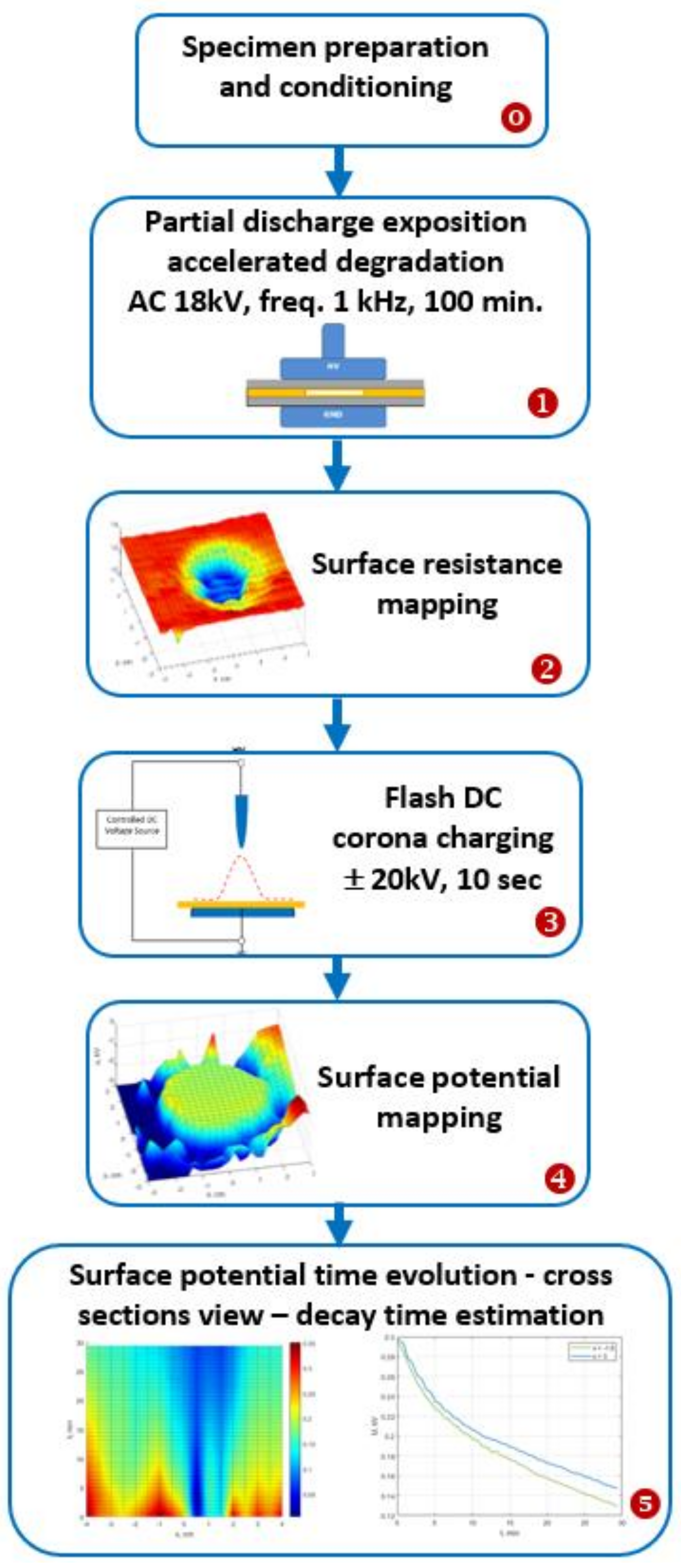
Figure 2.
Geometry of test specimen with embedded void.
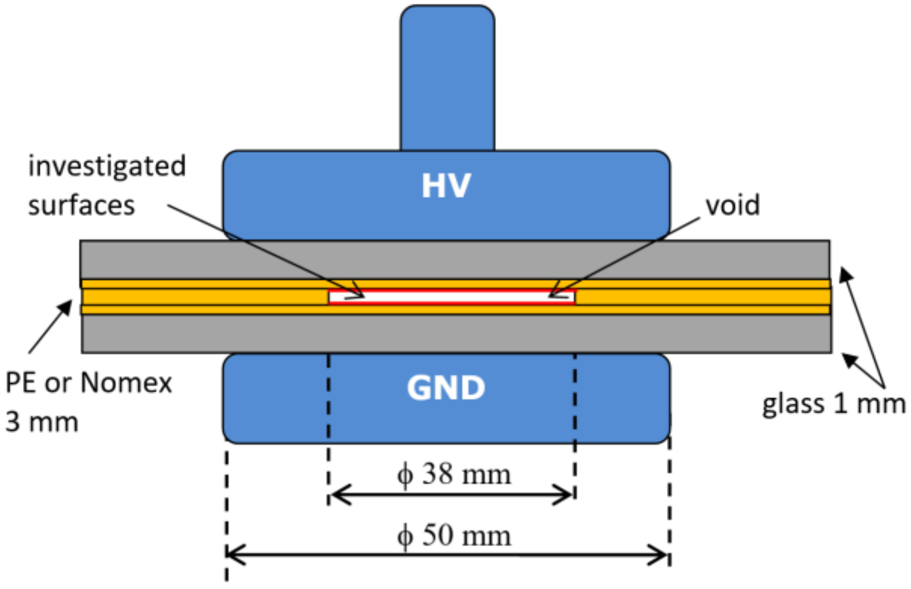
Figure 3.
Electrical exposure setup: (a) AC accelerated high-frequency deterioration; (b) DC charge sprinkling.
Figure 3.
Electrical exposure setup: (a) AC accelerated high-frequency deterioration; (b) DC charge sprinkling.

Figure 4.
Instrumentation for automatic surface-resistance and potential mapping.

Figure 5.
Surface-resistance mapping inside voids on PE (left column) and Nomex (right column) specimens (bottom sides): (a,b) map view; (c,d) 3D view; (e,f) cross-section view.
Figure 5.
Surface-resistance mapping inside voids on PE (left column) and Nomex (right column) specimens (bottom sides): (a,b) map view; (c,d) 3D view; (e,f) cross-section view.
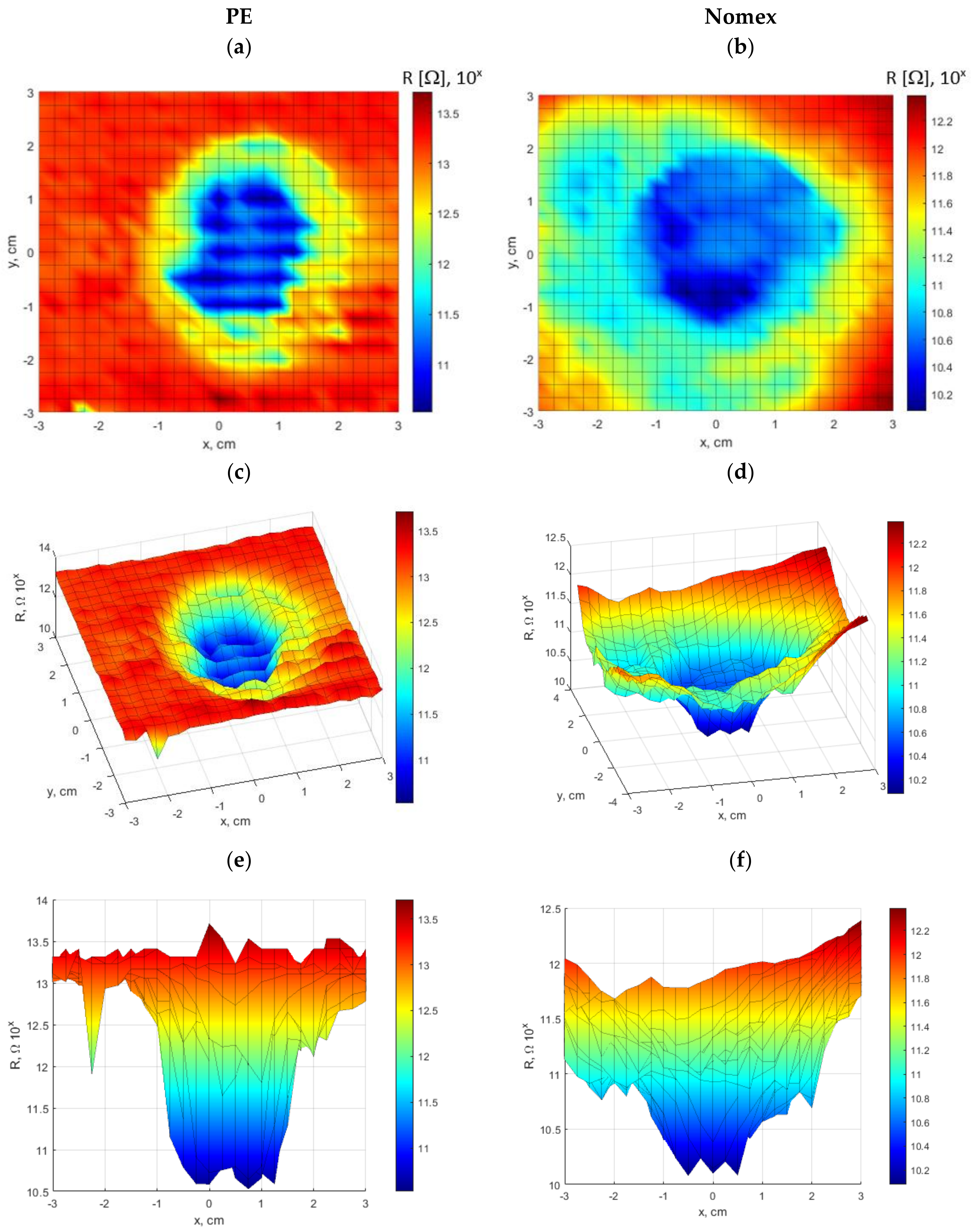
Figure 6.
Surface-potential mapping on void walls of PE specimens (bottom side): (a,c) map views; (b,d) 3D views; (a,b) negative polarity of corona charging; (c,d) positive polarity of corona charging.
Figure 6.
Surface-potential mapping on void walls of PE specimens (bottom side): (a,c) map views; (b,d) 3D views; (a,b) negative polarity of corona charging; (c,d) positive polarity of corona charging.
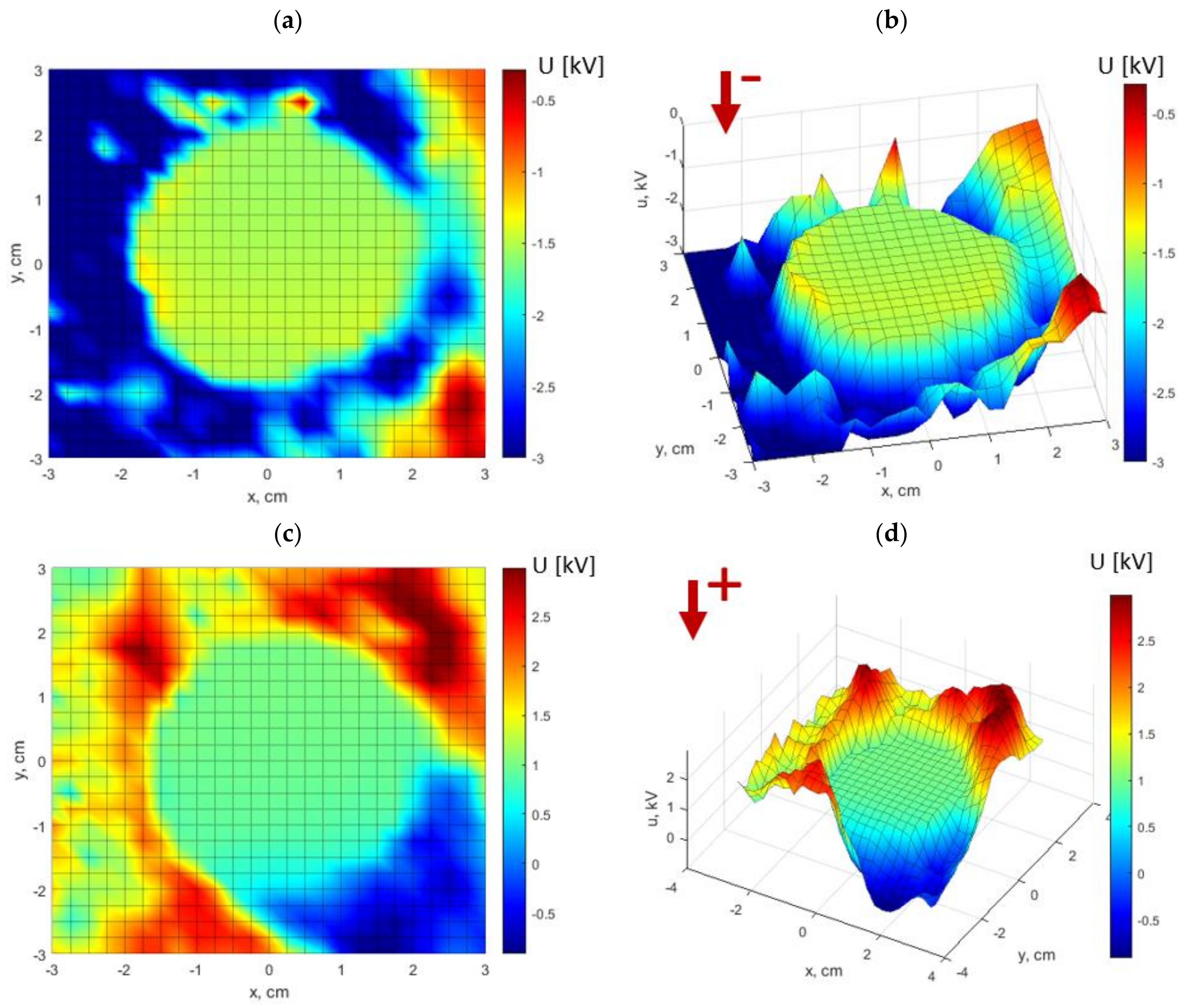
Figure 7.
Surface-potential mapping on void walls of Nomex specimens (bottom sides)—map view: (a) negative polarity of corona charging; (b) positive polarity of corona charging.
Figure 7.
Surface-potential mapping on void walls of Nomex specimens (bottom sides)—map view: (a) negative polarity of corona charging; (b) positive polarity of corona charging.
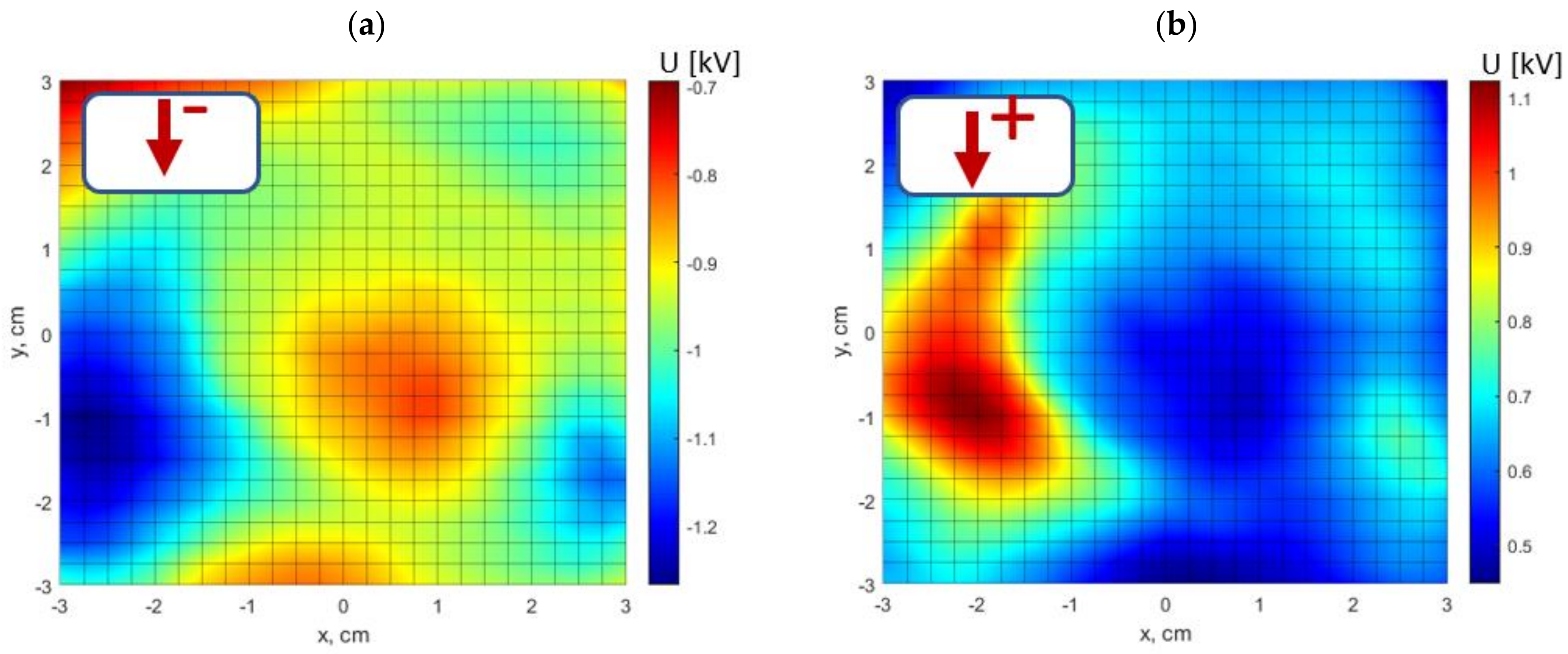
Figure 8.
Visualization of mapping effects on surface of deteriorated insulating material.
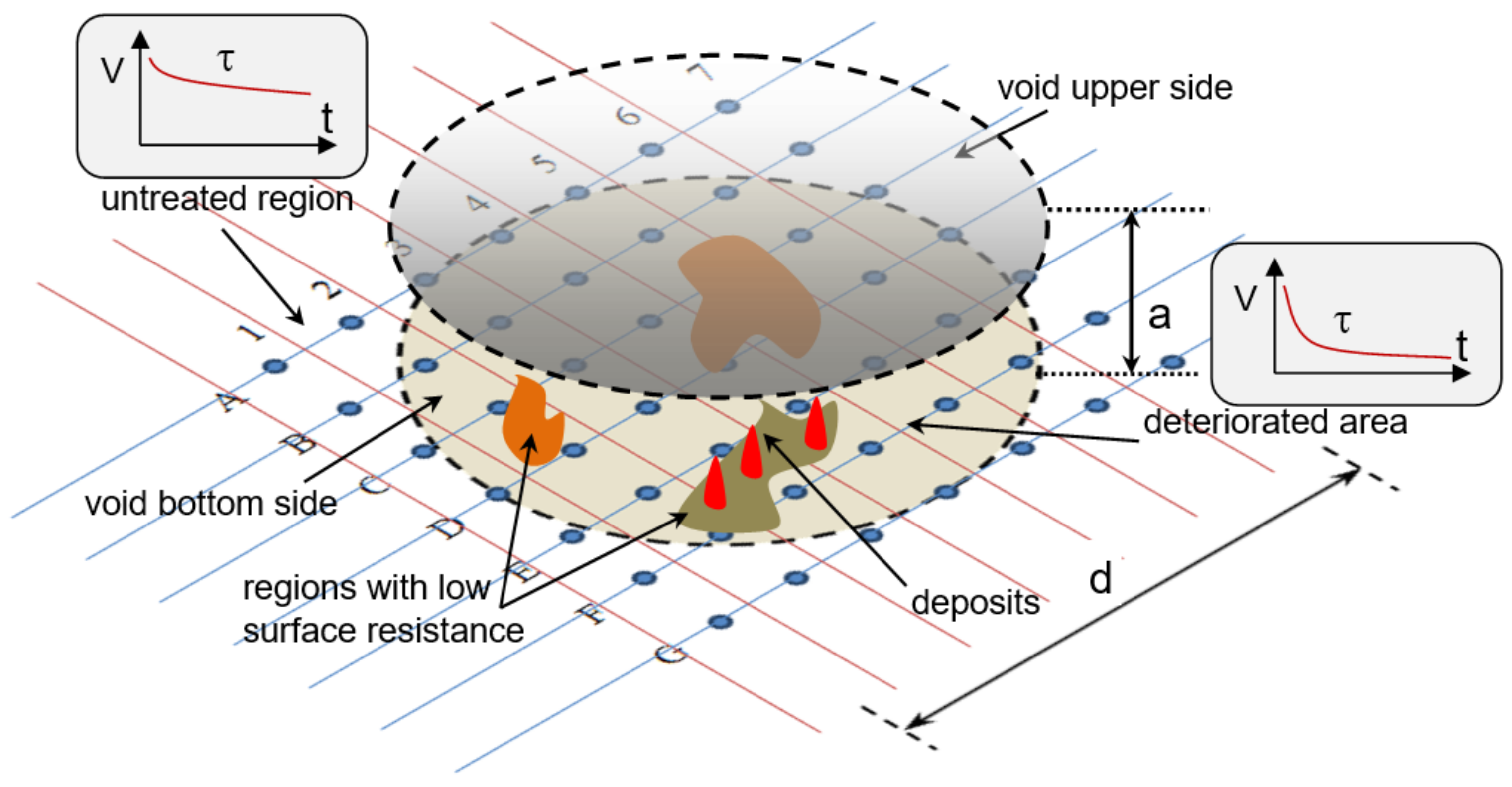
Figure 9.
Extracted void areas deteriorated by partial discharges in high-frequency accelerated test (1 kHz, 18 kV) based on surface-resistance mapping: (a) PE; (b) Nomex.
Figure 9.
Extracted void areas deteriorated by partial discharges in high-frequency accelerated test (1 kHz, 18 kV) based on surface-resistance mapping: (a) PE; (b) Nomex.

Figure 10.
Surface-resistivity mapping for PE specimen with applied thresholding (Table 2): thresholds are marked on top of each plot, and the degradation degree is expressed by Pi factor.
Figure 10.
Surface-resistivity mapping for PE specimen with applied thresholding (Table 2): thresholds are marked on top of each plot, and the degradation degree is expressed by Pi factor.

Figure 11.
Surface-resistivity mapping for Nomex specimen with applied thresholding (Table 2): thresholds are marked on top of each plot, and the degradation degree is expressed by Pi factor.
Figure 11.
Surface-resistivity mapping for Nomex specimen with applied thresholding (Table 2): thresholds are marked on top of each plot, and the degradation degree is expressed by Pi factor.

Figure 12.
Surface-potential mapping-time evolution for Nomex—cross-section alongside x-axis at y = 0: (a) planar mapping—negative charging; (b) potential decay at selected cross-sections; (c) planar mapping—positive charging; (d) potential decay at selected cross-sections (charge deposition over 10 s: (a,b) DC −20 kV; (c,d) +20 kV—white dashed lines represent time evolution cutting profiles).


Table 1.
Typical properties of Nomex Type 418 and PE specimens [18].
Table 1.
Typical properties of Nomex Type 418 and PE specimens [18].
| Nomex 418 | PE | |
|---|---|---|
| Dielectric Strength, AC [kV/mm] | 30 | 40 |
| Dielectric constant, dry | 2.3 | 2.2 |
| Dissipation factor | 0.006 | 0.0009 |
| Volume resistivity [Ω·m] | 1014 | 6 × 10¹⁵ |
| Surface resistivity [Ω] | 4 × 10¹³ | 5 × 10¹³ |
| Layer thickness [mm] | 0.96 = 8 × 0.12 | 1 |
Table 2.
Threshold levels and percentage shares (Pi) for PE and Nomex specimens.
| Thresholds Thhigh_i [Ω] Bottom Void Wall | PE Pi [%] | Thresholds Thhigh_i [Ω] Bottom Void Wall | Nomex Pi [%] |
|---|---|---|---|
| 1010 < R ≤ 1 × 10¹¹ | 17.0 | 109 < R ≤ 2.5 × 10¹⁰ | 14.4 |
| 1 × 10¹¹ < R ≤ 1 × 10¹² | 39.3 | 2.5 × 10¹⁰ < R ≤ 5 × 10¹⁰ | 55.4 |
| 1 × 10¹² < R ≤ 1 × 10¹³ | 42.6 | 5 × 10¹⁰ < R ≤ 7.5 × 10¹⁰ | 23.0 |
| 1 × 10¹³ < R ≤ 1 × 10¹⁴ | 1.1 | 7.5 × 10¹⁰ < R ≤ 1011 | 6.0 |
Disclaimer/Publisher’s Note: The statements, opinions and data contained in all publications are solely those of the individual author(s) and contributor(s) and not of MDPI and/or the editor(s). MDPI and/or the editor(s) disclaim responsibility for any injury to people or property resulting from any ideas, methods, instructions or products referred to in the content. |
© 2023 by the authors. Licensee MDPI, Basel, Switzerland. This article is an open access article distributed under the terms and conditions of the Creative Commons Attribution (CC BY) license (https://creativecommons.org/licenses/by/4.0/).
Share and Cite
MDPI and ACS Style
Florkowski, M.; Kuniewski, M. Partial Discharge-Originated Deterioration of Insulating Material Investigated by Surface-Resistance and Potential Mapping. Energies 2023, 16, 5973. https://doi.org/10.3390/en16165973
AMA Style
Florkowski M, Kuniewski M. Partial Discharge-Originated Deterioration of Insulating Material Investigated by Surface-Resistance and Potential Mapping. Energies. 2023; 16(16):5973. https://doi.org/10.3390/en16165973
Chicago/Turabian StyleFlorkowski, Marek, and Maciej Kuniewski. 2023. "Partial Discharge-Originated Deterioration of Insulating Material Investigated by Surface-Resistance and Potential Mapping" Energies 16, no. 16: 5973. https://doi.org/10.3390/en16165973
Note that from the first issue of 2016, this journal uses article numbers instead of page numbers. See further details here.