
Optimal Design of a Submodule Capacitor in a Modular Multilevel Converter for Medium Voltage Motor Drives


1
Department of Energy and Power Conversion Engineering, University of Science & Technology, Daejeon 34113, Republic of Korea
2
Electric Machines and Drives Research Center, Korea Electrotechnology Research Institute, Changwon 51543, Republic of Korea
*
Author to whom correspondence should be addressed.
Energies 2024, 17(2), 471; https://doi.org/10.3390/en17020471
Submission received: 7 November 2023
/
Revised: 4 January 2024
/
Accepted: 11 January 2024
/
Published: 18 January 2024
(This article belongs to the Special Issue Challenges and Research Trends in Modular Multilevel Converters)
Abstract
:This paper proposes an algorithm for determining the optimal capacitance by utilizing a mathematical model of a submodule (SM) capacitor in a modular multilevel converter (MMC) specifically for medium voltage motor drives (MVDs). By approximating the voltage fluctuation of the SM capacitor during low-frequency operation, it is feasible to ascertain the minimum capacitance required for the SM capacitor, ensuring that its voltage fluctuations remain within an acceptable limit that is predefined as a specified value. Moreover, the study considered the injection of both a high-frequency common-mode voltage (CMV) and a circulating current to alleviate the SM voltage fluctuation during the acceleration of motor drives. The effectiveness of the proposed method is validated through verification using time-domain simulation results obtained using the MATLAB/SIMULINK software and real-time simulation results acquired using the OPAL-RT simulator platform.
1. Introduction
Modular multilevel converters (MMCs) have become an attractive multilevel converter topology for medium-to-high-voltage and high-power applications owing to their advantages regarding modular design, low harmonic distortion of the output voltage, and low switching frequency [1,2,3,4,5]. Consequently, MMCs have been extensively used in various industrial applications, including high-voltage direct current (HVDC) transmission systems [6,7,8,9,10], static synchronous compensators (STATCOM) [11,12,13,14], and medium voltage motor drives (MVDs) [15,16,17,18,19,20,21,22,23,24]. In addition to the salient features, submodule (SM) capacitors exhibit substantial voltage fluctuations at low frequencies, necessitating the selection of a sufficiently large capacitance to minimize this variability. However, this causes the converter system to be oversized and expensive, thereby restricting the applicability of the MMC system. In theory, the voltage ripple in an SM capacitor is directly proportional to the amplitude of the output current and inversely proportional to the operating frequency. This results in a significant voltage ripple in the SM when the motor drives operate at low speeds, particularly during startup [25]. Owing to these considerations, numerous studies have been conducted to improve the dynamic performance of converter systems when motor drives operate at low speeds [17,18,25,26,27,28,29,30].
Injecting high-frequency sinusoidal waveforms of the common-mode voltage (CMV) and a circulating current into each arm results in a significant reduction in the voltage fluctuation of the SM capacitor [18,25,26]. Through this control strategy, the transfer of high-frequency components between the upper and lower arms enables more frequent charging and discharging of the SM capacitor, effectively suppressing voltage fluctuations without affecting the three-phase output currents (Figure 1). However, the injection of high-frequency components gives rise to a CMV on the motor side, leading to the potential harming of the motor winding and the deterioration of the motor bearings [17]. Furthermore, the incorporation of sinusoidal waveforms induces elevated current stress in each arm, leading to increased power loss. To alleviate the current stress in each arm, a high-frequency square-wave CMV and circulating current are injected into each arm as an alternative to sinusoidal high-frequency components [27]. Nevertheless, the use of a square-waveform CMV may lead to significant dv/dt issues at the motor terminal, posing a threat to the lifespan of motor bearings and rendering them unsuitable for practical applications. Similarly, the proposed method involves the introduction of a flying-capacitor MMC (FC-MMC) to alleviate arm current stress and SM capacitor voltage fluctuations without introducing a CMV to the motor winding [28,29,30].
Although employing a substantial capacitance can minimize SM voltage fluctuations, it results in the MMC system being oversized and expensive. Consequently, determining the appropriate size of the SM capacitor is crucial, as it establishes the minimum capacitance required to attain the optimal performance in the MMC-based motor drive system. The examination and evaluation of the SM capacitance in high-voltage direct current (HVDC) transmission systems using the MMC topology are presented in [31,32,33]. Merlin et al. introduced a mathematical model to predict the minimum required size of SM capacitors to maintain the voltage ripple within permissible limits [34]. In [35,36,37], SM capacitance was determined by assessing the arm energy fluctuation. However, these approaches only size the SM capacitance by considering the fundamental frequency components of an MMC system.
This paper proposes a mathematical model for sizing SM capacitors by estimating the SM voltage to ensure that the SM voltage fluctuates within an allowable limit during low-frequency operation for motor drive applications. The main technical contributions of this study are as follows.
- The approach of utilizing a high-frequency CMV and circulating current injection to minimize SM capacitor voltage fluctuations during low-speed or standstill operations of the motor drive is mathematically explained in detail.
- An algorithm is formulated to estimate the SM capacitor voltage ripple, which is employed to optimize the SM capacitance in accordance with the system specifications for the allowable SM capacitor voltage ripple limit (Δvlim).
The remainder of the paper is structured as follows: Section 2 outlines the MMC circuit and its operation and provides a suppression of the SM voltage ripple during low-frequency operation. In Section 3, we introduce the proposed optimal algorithm for designing SM capacitors based on estimating the SM voltage fluctuations under variable frequency operations. Section 4 and Section 5 demonstrate the efficacy of the proposed method through time-domain simulations using MATLAB/SIMULINK R2021a software and real-time simulations using the Opal-RT platform. Finally, Section 6 summarizes the key contributions and conclusions of this study.
2. Circuit and Operation of Modular Multilevel Converter
2.1. Circuit Operation
A schematic representation of a three-phase MMC connected to an induction motor (IM) is shown in Figure 1. The MMC comprises three phases, with each phase composed of two arms. The arm linked to the positive bar is termed the upper arm, whereas the arm connected to the negative bar is referred to as the lower arm. Each arm consists of Nsm-identical SMs connected in series with a buffer inductor (Larm) designed to control the circulating currents within the converter arising from voltage disparities between the arms. The SM circuit can take the form of a half-bridge (HB), full-bridge (FB), or flying-capacitor power circuit. In this investigation, the HB circuit was employed for its simplicity, featuring two power semiconductor devices, denoted as IGBT T1 and T2, along with an isolated capacitor (Cdc) and freewheeling diodes.
The configuration and function of the HB-SM are shown in Figure 2. The SM capacitor (Cdc) is regulated to be charged, discharged, or bypassed based on the direction of the arm current and switching state of the IGBT devices. During the ON state of S1, the SM capacitor voltage (vsm) increases in the positive direction of the arm current (iarm > 0), indicating the charged mode, and decreases in the negative direction of the arm current (iarm < 0), signifying the discharged mode, as illustrated in Figure 2a,b, respectively. In the OFF state of S1, the SM capacitor voltage remains constant, representing the bypassed mode, irrespective of the arm current direction, as illustrated in Figure 2c,d.
2.2. Voltage Ripple Reduction under Low-Frequency Operation
Assuming that the output voltage (vx) and current (ix) exhibit symmetrical sinusoidal waveforms, they can be represented as per Equation (1):
where vx and ix correspond to the output voltage and output current of phase x, respectively (x = a, b, and c represent phases a, b, and c); Vx and Ix denote the amplitudes of the output voltage and current; while δx represents the initial phase angle of phase x (with a = 0, b = −2π/3, and c = 2π/3); and ϕx signifies the phase shift between voltage and current.
In accordance with Kirchhoff’s voltage law (KVL), the voltages across the upper and lower arms (vxP and vxN) can be formulated as expressed in Equation (2). By substituting the three-phase output voltage from Equation (1) into the upper and lower arm voltage expressions in Equation (2), the arm voltages can be represented as expressed in Equation (3).
where vxP and vxN represent the upper and lower arm voltages of phase x, and VDC denotes the DC-link voltage.
The upper arm current and lower arm current (ixP and ixN) of phase x can be expressed as shown in (4).
where ixP and ixN are the upper and lower arm currents of phase x, and icirc,x is the circulating current of phase x.
As previously noted, the SM voltage ripple experiences significant fluctuations during the startup operation of motor drives, owing to its inverse proportionality to the frequency of operation. To mitigate this voltage fluctuation in the SM, a high-frequency CMV denoted as vh, along with the circulating current (ih), is introduced into each arm. This injection enhances the exchange of high-frequency components between the arms of the converter. The introduced high-frequency voltage and current are expressed as indicated in Equations (5) and (6).
where vh and ih represent the high-frequency voltage and current injected into each arm, respectively; Vh and Ih denote the amplitudes of the injected high-frequency voltage and current, respectively; ωh represents the frequency of vh; and ih, Mmax is a coefficient representing the modulation margin (Mmax = 0.85–0.95).
The upper and lower arm voltages (vxP and vxN), which account for the introduced high-frequency voltage (vh), can be obtained as expressed in Equation (7).
Moreover, the upper and lower arm currents (ixP and ixN), factoring in the injected high-frequency circulating current (ih), are represented in Equation (8). It is important to highlight that the frequency (fh) must be chosen to be less than one-tenth of the switching frequency of the converter (fh ≤ fsw/10) to ensure effective controllability.
The instantaneous powers of the upper and lower arms (PxP, PxN) can be determined, as outlined in Equation (9), and derived from Equation (10) by multiplying the arm voltage and current from Equations (7) and (8), respectively.
where PxP and PxN represent the instantaneous power of the upper and lower arm in phase x, respectively.
The powers in the upper and lower arms consist of fundamental, second, and high-frequency components injected into each arm to mitigate the SM voltage ripple, as expressed in Equation (10). The high-frequency components have a minimal impact on the voltage ripple, which is primarily influenced by the fundamental and second harmonics [38]. Consequently, the high-frequency components were disregarded, and only the fundamental and second-order harmonic components were considered, as indicated in Equation (11).
At a steady state, the first and second terms in Equation (11) are equal because of the power balance between the DC and AC sides. The remaining terms consist of both fundamental and high-frequency components, representing the power exchange within the converter induced by the AC and DC components of the circulating currents, respectively, leading to fluctuations in the SM capacitor voltage. Based on these terms, the DC circulating current icircx,dc can be calculated as expressed in Equation (12).
As expressed in Equation (11), the powers in the upper and lower arms are similar, with certain terms having opposite signs, and there is no difference between the upper and lower arms in the SM voltage fluctuation control. For simplicity, only the upper arm power was examined to mitigate the SM voltage fluctuation.
where PxP,rpl represents the power ripple of phase x in the upper arm.
To mitigate the SM voltage fluctuation, the ripple in the upper arm power is regulated to zero (PxP,rpl = 0). By substituting the circulating current from Equation (12) into the arm power ripple in Equation (13), the magnitude of the high-frequency components can be determined, as expressed in Equation (14). The magnitude of the high-frequency current injected into each arm can be calculated as expressed in Equation (15).
By substituting the magnitude of the injected high-frequency current from Equation (15) into Equation (6), the injected high-frequency current can be represented as indicated in Equation (16).
Consequently, the voltage fluctuation in the SM capacitor is alleviated during low-frequency operations through the injection of a high-frequency current into each arm of the MMC system.
3. Design SM Capacitor in Low-Speed Range of Medium Voltage Motor Drives
In this section, an optimal design algorithm for the SM capacitor is presented, which relies on the estimation of the SM voltage ripple during the low-frequency operation of motor drives. The proposed method ensures that the voltages of the SM capacitors fluctuate within a predefined limit by considering the voltage ripple requirements of the system.
3.1. Estimation of Submodule Voltage Fluctuation
The power ripple in the upper arm can be obtained by substituting Equation (12) into Equation (13), as expressed in Equation (17). Similarly, the power ripple in the lower arm can be represented by Equation (18). Subtracting the power ripple of the lower arm from that of the upper arm yields the power ripple for the corresponding phase, as expressed in Equation (19).
where PxN,rpl represents the power ripples of phase x in the lower arm.
Integrating the power ripple of the phase (Px,rpl) from Equation (19), the energy ripple of phase x (Ex,rpl) considering the injected high-frequency components can be obtained, as indicated in Equation (20).
where Ex,p−p represents the energy ripple of phase x.
Assuming that the energy distributed among each SM is equal, the relationship between the energy ripple of phase x and the SM capacitor voltage ripple can be established, as expressed in (21).
where Ex,p−p is the energy ripple of phase x in the upper arm, and Δvp−p is the peak–peak voltage ripple of the SM capacitor.
By substituting the energy ripple from Equation (21) into Equation (20), the SM voltage ripple can be derived, as expressed in Equation (22). The process of estimating the SM voltage fluctuation based on the energy fluctuation is illustrated in Figure 3.
3.2. Optimal Sizing Algorithm of the SM Capacitor
Figure 4 illustrates the optimal design algorithm for SM capacitance, employing a mathematical model to estimate the SM voltage fluctuation during low-frequency operations. In addition, the voltage ripple limit (∆vc,lim) of the SM capacitor is predefined as a system requirement, which ensures that the SM capacitor voltage fluctuates within an allowable limit.
Initially, the SM capacitance is selected to guarantee that the voltage fluctuation of the SM capacitor remains within the specified limit as per the system requirement (∆vp−p ≤ ∆vlim). It is important to emphasize that the value of Δvlim may vary based on the specific requirements of the different systems. Consequently, the minimum capacitance must adhere to the given constraint, as expressed by Equation (23).
![Energies 17 00471 g004]()
Figure 4.
Sizing SM capacitor algorithm.
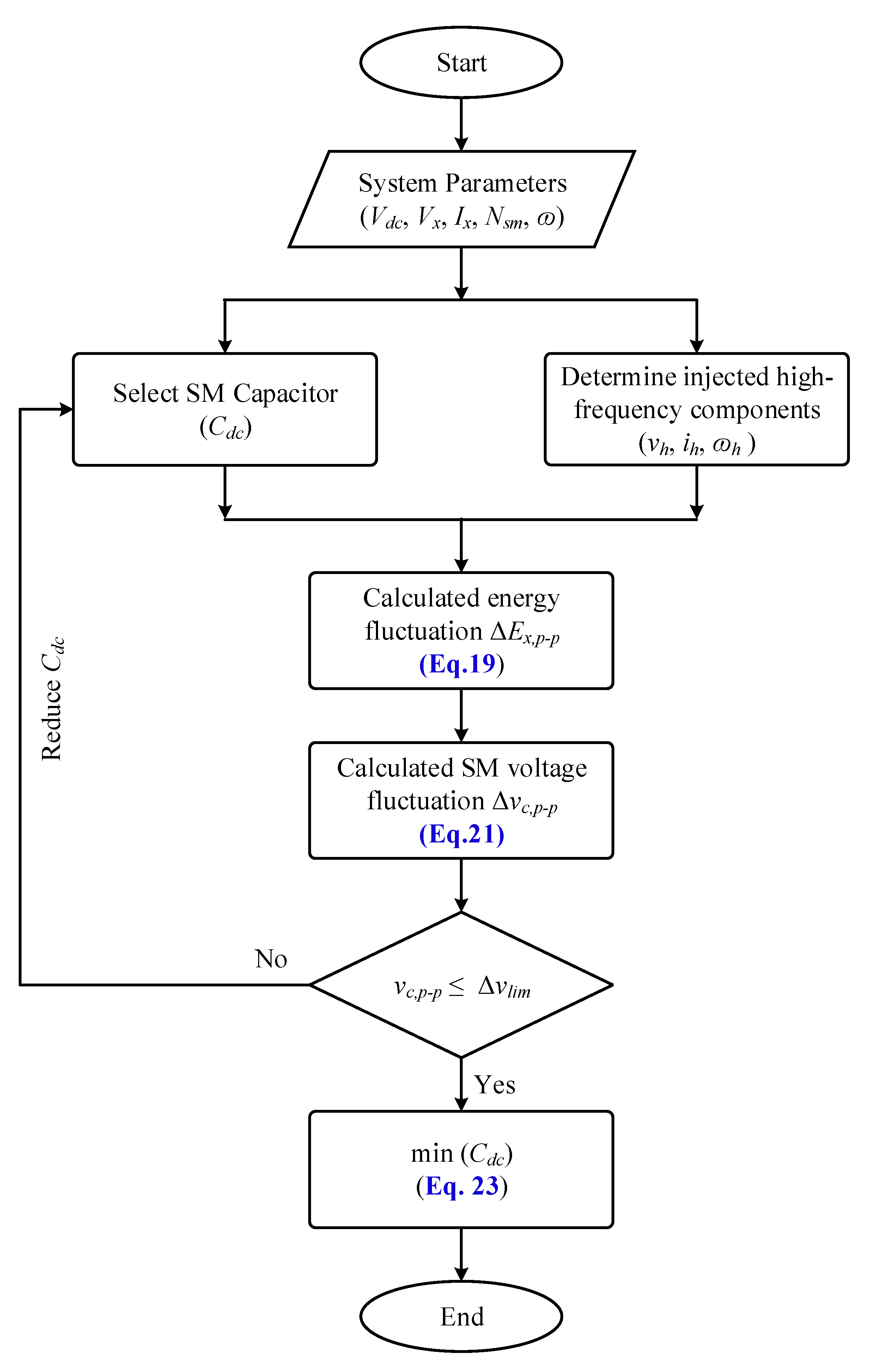
Based on the system parameters and the high-frequency components injected into each arm during low-frequency operations, the energy ripple and SM voltage fluctuation can be estimated using the outlined procedure of the proposed algorithm, as illustrated in Figure 3. By assessing the SM voltage ripple against the defined voltage ripple limit, the optimal capacitance of the SM capacitor can be identified using the proposed algorithm procedure outlined in Figure 4. Figure 5 depicts the changes in the SM capacitor voltage fluctuation (Δvp−p) under the influence of the injected high-frequency components, considering the variations in capacitance and operational frequency. Furthermore, the system permits SM capacitor voltages to fluctuate within an acceptable range of Δvlim = 10%. For an operational frequency of fn = 10 Hz, the SM voltage ripple can reach 2.8% with a higher SM capacitance of Cdc = 3500 µF. However, the system can be optimized by selecting an SM capacitance of Cdc = 1000 µF while still meeting the system requirement of Δvlim.
If the SM voltage ripple exceeds the voltage limit (∆vc,p−p > ∆vlim), the SM capacitance must be increased to mitigate the voltage ripple value. If the SM voltage ripple is lower than the voltage limit (∆vc,p−p < ∆vlim), the SM capacitance must be reduced to optimize the capacitance value. This process is iterated until the voltage ripple approaches the voltage ripple limit (∆vc,p−p ≈ ∆vlim), leading to the determination of the optimal SM capacitance. In this investigation, a voltage ripple limit of ∆vlim = 10% was selected, corresponding to a rated SM voltage of vc,rated = 1600 V, which is established as an acceptable limit for the SM capacitor voltage. Consequently, the SM capacitance was selected as Cdc = 1000 µF to ensure that the SM voltage fluctuation was ∆vlim ≤ 10%.
3.3. SM Voltage Balancing Control
Figure 6 depicts the SM capacitor voltage balancing control employing the high-frequency injection method. This method encompasses phase average voltage control, individual SM voltage control, and SM voltage reference generation [27]. The average phase voltage (), expressed in Equation (24), is regulated to track the reference value of the average voltage () using a proportional–integral (PI) controller, as illustrated in Figure 6a. The output from the phase voltage controller () serves as the reference for the circulating current controller. Additionally, the circulating current (icir,x) was controlled to adhere to the circulating current reference while incorporating a high-frequency component (ih).
where is the capacitor voltage average of phase x; Vcj,xu and Vcj,xl are the jth SM voltages of the upper and lower arms, respectively; and Nsm is the number of SM per arm.
The control of the individual SM voltages is presented in Figure 6b, where each SM voltage is regulated to track the voltage reference (). Furthermore, the direction of the arm currents (ixP and ixN) determines the polarity of the controller output, which can be employed for SM voltage reference generation. A block diagram illustrating the SM voltage reference generation in the upper and lower arms with a high-frequency common-mode voltage (CMV) injected into each arm is shown in Figure 6c and expressed mathematically in Equations (25) and (26), respectively.
![Energies 17 00471 g006]()
Figure 6.
SM voltage balancing control based on the high-frequency injection method: (a) phase voltage balancing and circulating current control, (b) individual SM voltage control, (c) SM voltage reference generation.
Figure 6.
SM voltage balancing control based on the high-frequency injection method: (a) phase voltage balancing and circulating current control, (b) individual SM voltage control, (c) SM voltage reference generation.

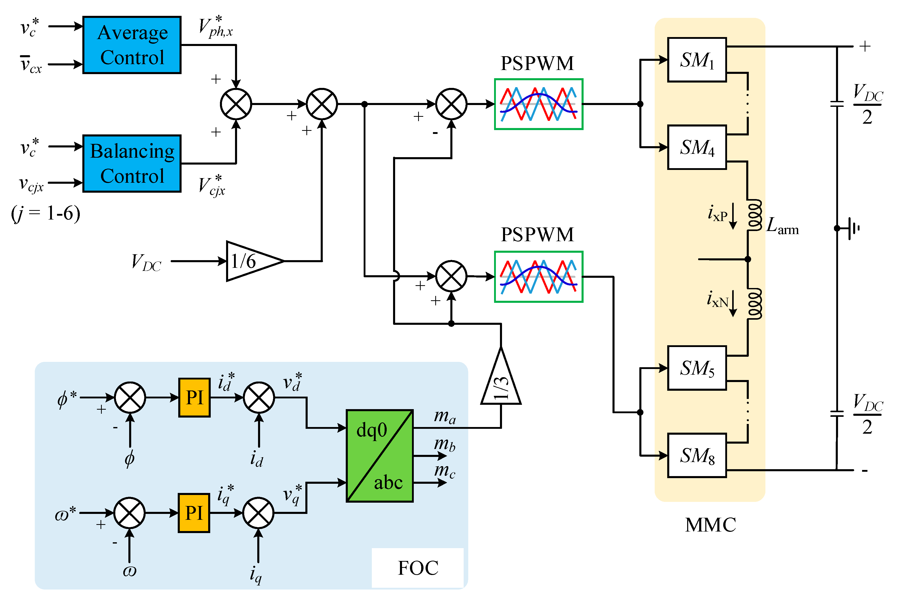
3.4. Overall System Control
Figure 7 illustrates a comprehensive control block diagram of the MMC-based motor drive system, encompassing both motor control and converter control. Motor drive control employs the field-oriented control (FOC) method, which consists of an outer loop controller and an inner loop controller. In the outer loop controller, the actual motor speed (ω) and rotor flux (ψ) are regulated to track the reference values of ɷ* and ψ*, thus providing the direct–quadrature (d-q) axis current references ( and ) and stator current angle (θr). In the inner controller, the measured stator current (id and iq) is regulated to follow the reference values and . The output of the FOC control provides voltage commands (ma, mb, and mc), which are utilized to generate modulation signals for SM voltage reference generation. Further details regarding the FOC method for controlling motor drives using the d-q reference frame can be found in [39].
Regarding MMC control, the control strategy for SM voltage balancing encompasses the average SM voltage balancing control, individual SM voltage balancing control, and circulating current control, contributing to the generation of the SM voltage reference. A detailed discussion of the components of the SM capacitor voltage balancing control is provided in Section 3.3. Additionally, the high-frequency common-mode voltage (CMV) injection method was employed to mitigate the SM voltage fluctuation during the standstill/low-speed period of the motor drives. The phase-shifted pulse-width modulation (PSPWM) scheme is utilized to generate the switching state of the power switching devices, as depicted in Figure 7.
Figure 7.
Overall control block diagram of the MMC system.
4. Simulation Results
In this section, we verify the efficiency of the proposed approach in reducing the size of the SM capacitor using time-domain simulation with MATLAB/SIMULINK software and real-time simulation using the OPAL/RT platform. The motor converter system consisted of an induction motor (IM) and a three-phase MMC with 3 SMs per arm, totaling 18 SMs. The system parameters are listed in detail, as shown in Table 1.
The variation in the SM voltage ripple, according to the variation in the operating frequency and considering high-frequency components injected into each arm to eliminate the SM capacitor voltage fluctuation, is illustrated in Figure 8. Theoretically, the SM voltage fluctuation is inversely proportional to the operation frequency, resulting in significant voltage fluctuation at a very low frequency operation (fn = 1 Hz) without injecting high-frequency CMV (Δvp−p = 16,074 V), reducing significantly (Δvc,p−p = 159.155 V) with the support of injected high-frequency components, as shown in Figure 8. Therefore, the SM capacitor voltage ripple must be mitigated during the standstill/low-speed operation of the motor drive to ensure a high performance of the system.
The effectiveness of the proposed algorithm for estimating SM voltage fluctuations is validated by comparing the estimated SM capacitor voltage fluctuation, as defined in Equation (22), and the real values of the SM voltages in the upper arm (vcu) and lower arm (vcl). This comparison is depicted as shown in Figure 9a,b. It is evident that the estimated SM voltage, indicated by the red line, closely tracked the real values of the individual SM voltages in terms of both shape and magnitude. The simulation involved high-frequency components injected at a very low motor speed, with four SMs integrated into each converter arm and a DC-link voltage of 8000 V. The proposed algorithm exhibited excellent efficiency in estimating SM voltage fluctuations, with an error of less than 1%, as illustrated in Table 2 and Figure 10.
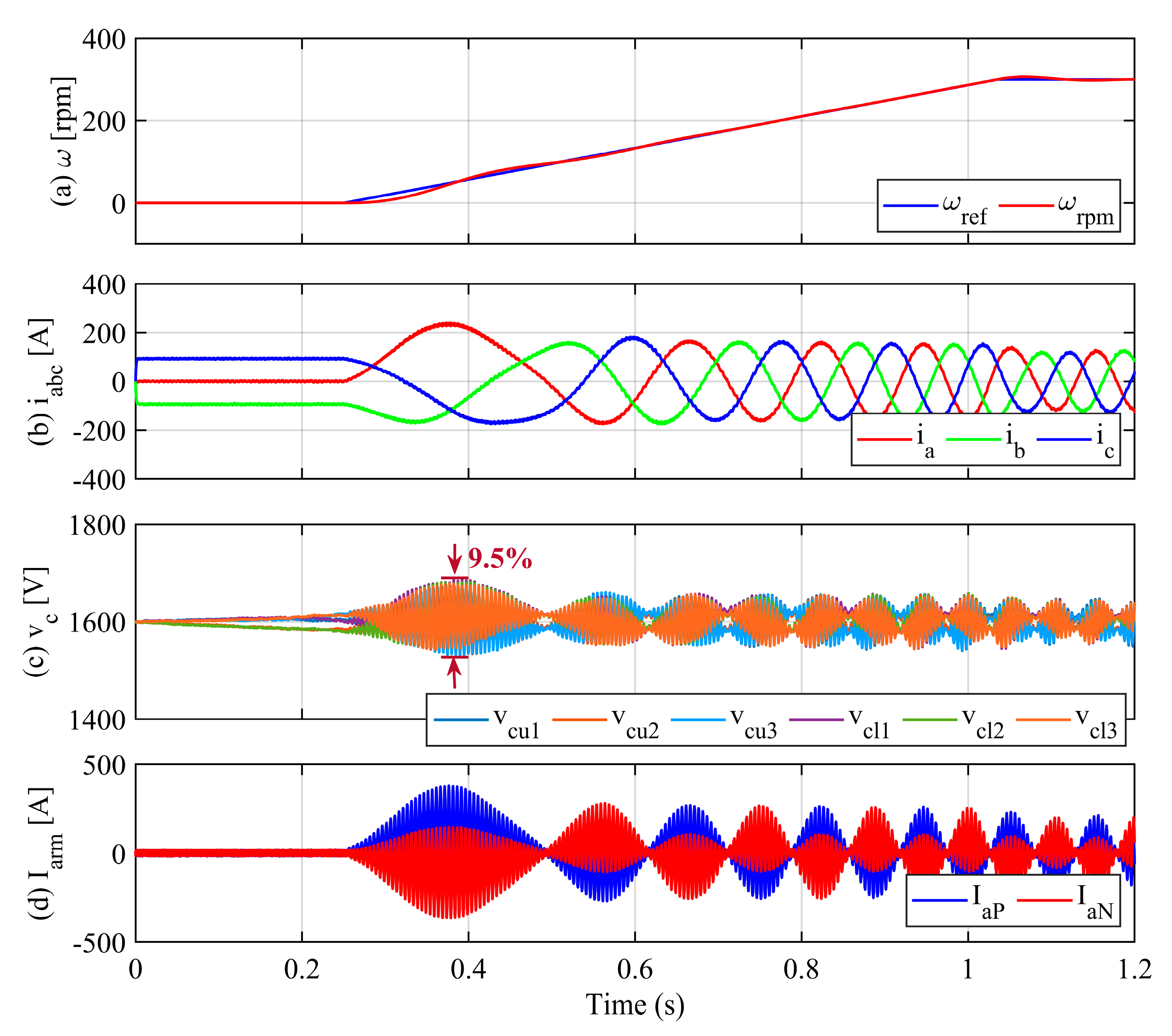
Figure 11 presents a recommendation for optimizing the SM capacitance at various operating frequencies using the proposed algorithm, based on the predefined system requirement for the SM voltage ripple limit (Δvlim). Assuming that the system allows for a maximum voltage ripple of Δvlim = 10%, the SM capacitance can be designed as Cdc = 1000 µF, as illustrated in Figure 11. The performance of the MMC-based motor drive system, considering the optimal SM capacitance of Cdc = 1000 µF and a high-frequency CMV injection, is shown in Figure 12. With the selected SM capacitance of Cdc = 1000 µF, the SM capacitor voltages were maintained in balance at the rated voltage of 1600 V, ensuring that the voltage fluctuations remained within the acceptable range defined by the system requirement of Δvlim.

Table 2.
Performance comparison of SM voltage ripple estimation method.
| Frequency [fn] | Voltage Ripple Estimation | Real SM Voltage Ripple |
|---|---|---|
| 5 Hz | 9.8% | 9.5% |
| 10 Hz | 8.6% | 8.1% |
| 15 Hz | 6% | 6.6% |
| 20 Hz | 5.4% | 5.8% |
| 25 Hz | 3.6% | 4.2% |
| 30 Hz | 2.2% | 2.9% |
Figure 9.
The performance of SM voltage estimation algorithm: (a) upper arm SM capacitor voltage, (b) lower arm SM capacitor voltage.
Figure 9.
The performance of SM voltage estimation algorithm: (a) upper arm SM capacitor voltage, (b) lower arm SM capacitor voltage.
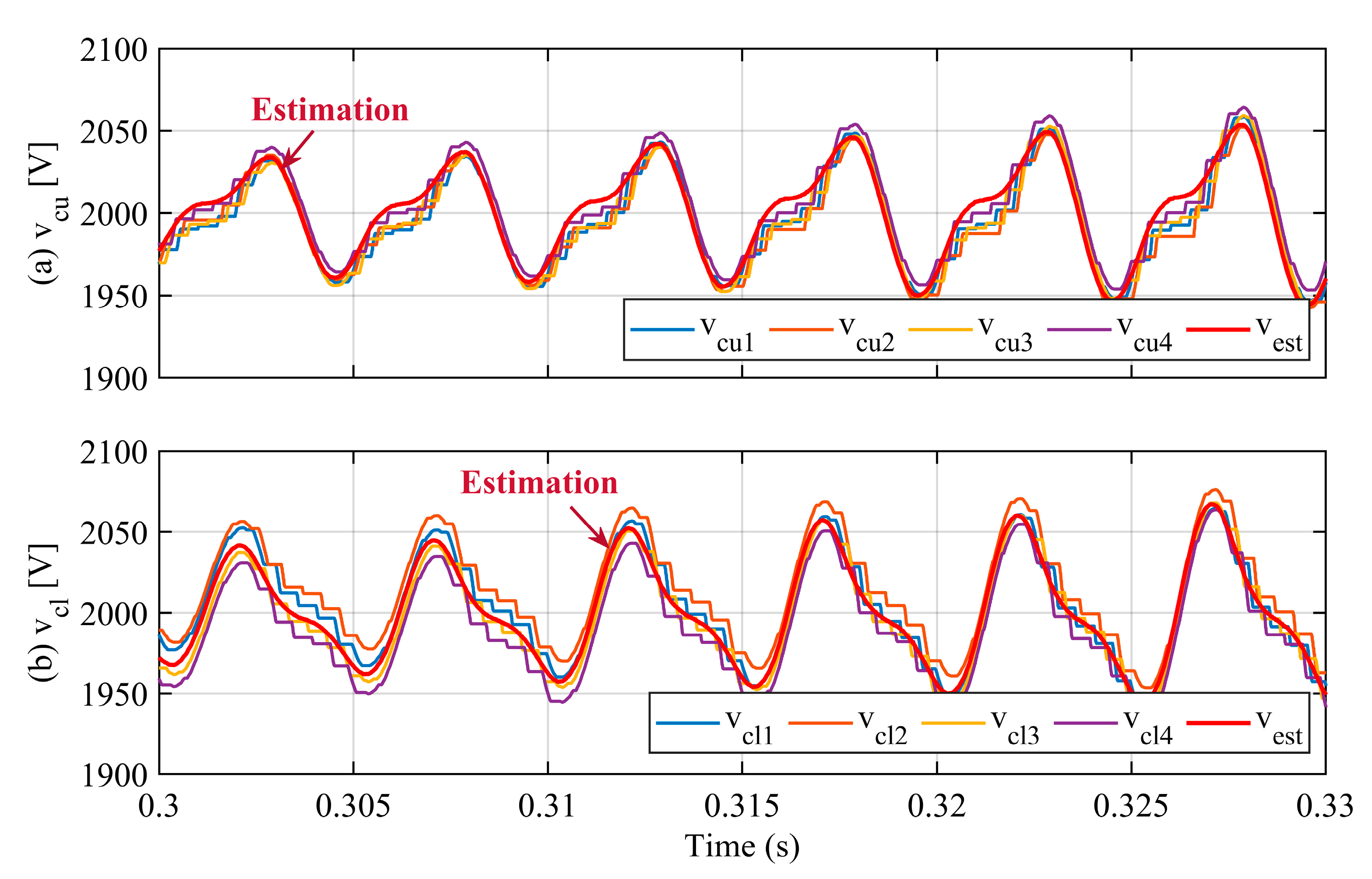
Figure 10.
Performance comparison of SM voltage ripple estimation method.

Figure 11.
Design of SM capacitance at different operating frequencies based on the predetermined voltage ripple limit (Δvlim).
Figure 11.
Design of SM capacitance at different operating frequencies based on the predetermined voltage ripple limit (Δvlim).

Figure 12.
Performance of the MMC with proposed SM capacitance selection: (a) motor speed, (b) three-phase current, (c) SM capacitor voltage, (d) arm currents.
Figure 12.
Performance of the MMC with proposed SM capacitance selection: (a) motor speed, (b) three-phase current, (c) SM capacitor voltage, (d) arm currents.
5. Real-Time Simulation
In this section, we evaluate the effectiveness of the proposed algorithm through real-time simulations using an OPAL-RT 5707 real-time simulator. These simulations ensured that computations occurred in real-time and were consistent with the results obtained from the hardware setup. The system configuration of the real-time simulator is illustrated in Figure 13, consisting of an OPAL-RT5707 real-time simulator, an RT-Lab target PC, an interface PC, and an oscilloscope. Initially, the proposed algorithm was conducted on the MATLAB/SIMULINK platform, seamlessly integrated into RT-LAB. Subsequently, real-time simulations were conducted using multiple cores. It is important to note that the OPAL-RT/FPGA analog output is limited to a range of ±16 V, requiring the application of a scaling factor for the effective visualization of the analog output waveforms.
Figure 14 illustrates the effectiveness of the proposed algorithm in estimating the voltage of the SM capacitor. The estimation, denoted by (22), was compared with the actual SM capacitor voltage. Owing to equipment constraints, only one SM voltage in both the upper and lower arms was compared with its estimated value. As shown in Figure 14a,b, the red lines representing the estimated SM capacitor voltage closely track the blue lines representing the real SM capacitor voltage. This observation validates the robust performance of the proposed algorithm for accurately estimating SM capacitor voltages.
Figure 13.
Establishment of a real-time simulation in laboratory using OPAL-RT simulator.

With the estimated SM capacitor voltage shown in Figure 14, the optimal SM capacitance of Cdc = 1000 μF was selected to ensure that the SM capacitor voltage fluctuated within the predefined range of the system specification. The performance of the proposed algorithm in fine-tuning the capacitance of the SM was evaluated at exceptionally low motor speeds of ω = 150 rpm using a real-time simulator, as shown in Figure 15. As indicated in Figure 15b, the voltages across the SM capacitors were maintained at equilibrium at the rated voltage of vc,rated = 1600 V, and the fluctuations in the SM capacitor voltages remained within 10%. This demonstrates compliance with the system requirements specifying Δvlim = 10%.
6. Conclusions
This paper proposes an optimal design algorithm to determine the optimal capacitance of SM capacitors in an MMC, using a proposed SM voltage ripple estimation algorithm to ensure that the SM voltages fluctuate within an acceptable range during low-frequency operations. Additionally, the concept of high-frequency CMV and circulating current injected into each arm has been conducted to minimize SM capacitor voltage fluctuations during low-speed or standstill operations of motor drives. Consequently, the proposed algorithm demonstrates exceptional precision, predicting the SM capacitor voltage ripple with a variance of less than 1%. The effectiveness of the proposed method was verified using time-domain simulation results with MATLAB/SIMULINK software and real-time simulation results with the OPAL-RT simulator platform. The simulation results demonstrate that the capacitance value obtained through the proposed optimal design algorithm guarantees that the SM capacitor voltage fluctuates within an acceptable range of Δvlim = 10%.
Author Contributions
V.-T.N. was responsible for the simulation, analysis, original draft writing, paper modification, and response to the reviewers. J.-W.K. and J.-W.L. reviewed the paper and provided advice on improving the paper’s quality. B.-G.P. supervised many aspects of this research including project administration, funding acquisition, and methodology development. He also conceived the original idea for the methodology and was responsible for reviewing and editing. All authors have read and agreed to the published version of the manuscript.
Funding
This research was supported by the Korea Electrotechnology Research Institute (KERI) Primary Research Program through the National Research Council of Science and Technology (NST) funded by the Ministry of Science and ICT: No. 24A01057.
Data Availability Statement
The data presented in this study are available on request from the corresponding author. The data are not publicly available due to confidentiality reasons from project.
Conflicts of Interest
The authors declare no conflicts of interest.
References
- Debnath, S.; Qin, J.; Bahrani, B.; Saeedifard, M.; Barbosa, P. Operation, Control, and Applications of the Modular Multilevel Converter: A Review. IEEE Trans. Power Electron. 2015, 30, 37–53. [Google Scholar] [CrossRef]
- Antonopoulos, A.; Ängquist, L.; Nee, H.P. On dynamics and voltage control of the modular multilevel converter. In Proceedings of the 2009 13th European Conference on Power Electronics and Applications, EPE’09, Barcelona, Spain, 8–10 September 2009; pp. 1–10. [Google Scholar]
- Dekka, A.; Wu, B.; Fuentes, R.L.; Perez, M.; Zargari, N.R. Evolution of Topologies, Modeling, Control Schemes, and Applications of Modular Multilevel Converters. IEEE J. Emerg. Sel. Top. Power Electron. 2017, 5, 1631–1656. [Google Scholar] [CrossRef]
- Perez, M.A.; Bernet, S.; Rodriguez, J.; Kouro, S.; Lizana, R. Circuit Topologies, Modeling, Control Schemes, and Applications of Modular Multilevel Converters. IEEE Trans. Power Electron. 2015, 30, 4–17. [Google Scholar] [CrossRef]
- Kouro, S.; Malinowski, M.; Gopakumar, K.; Pou, J.; Franquelo, L.G.; Wu, B.; Rodriguez, J.; Perez, M.A.; Leon, J.I. Recent Advances and Industrial Applications of Multilevel Converters. IEEE Trans. Ind. Electron. 2010, 57, 2553–2580. [Google Scholar] [CrossRef]
- Saeedifard, M.; Iravani, R. Dynamic Performance of a Modular Multilevel Back-to-Back HVDC System. IEEE Trans. Power Deliv. 2010, 25, 2903–2912. [Google Scholar] [CrossRef]
- Nami, A.; Liang, J.; Dijkhuizen, F.; Demetriades, G.D. Modular Multilevel Converters for HVDC Applications: Review on Converter Cells and Functionalities. IEEE Trans. Power Electron. 2015, 30, 18–36. [Google Scholar] [CrossRef]
- Gnanarathna, U.N.; Gole, A.M.; Jayasinghe, R.P. Efficient Modeling of Modular Multilevel HVDC Converters (MMC) on Electromagnetic Transient Simulation Programs. IEEE Trans. Power Deliv. 2011, 26, 316–324. [Google Scholar] [CrossRef]
- Peralta, J.; Saad, H.; Dennetière, S.; Mahseredjian, J.; Nguefeu, S. Detailed and Averaged Models for a 401-Level MMC-HVDC System. IEEE Trans. Power Deliv. 2012, 27, 1501–1508. [Google Scholar] [CrossRef]
- Guan, M.; Xu, Z. Modeling and Control of a Modular Multilevel Converter-Based HVDC System under Unbalanced Grid Conditions. IEEE Trans. Power Electron. 2012, 27, 4858–4867. [Google Scholar] [CrossRef]
- Akagi, H. Classification, Terminology, and Application of the Modular Multilevel Cascade Converter (MMCC). IEEE Trans. Power Electron. 2011, 26, 3119–3130. [Google Scholar] [CrossRef]
- Hagiwara, M.; Maeda, R.; Akagi, H. Negative-Sequence Reactive-Power Control by a PWM STATCOM Based on a Modular Multilevel Cascade Converter (MMCC-SDBC). IEEE Trans. Ind. Appl. 2012, 48, 720–729. [Google Scholar] [CrossRef]
- Pereira, M.; Retzmann, D.; Lottes, J.; Wiesinger, M.; Wong, G. SVC PLUS: An MMC STATCOM for network and grid access applications. In Proceedings of the 2011 IEEE PES Trondheim PowerTech: The Power of Technology for a Sustainable Society, POWERTECH 2011, Trondheim, Norway, 19–23 June 2011; pp. 1–5. [Google Scholar] [CrossRef]
- Lee, C.T.; Wang, B.S.; Chen, S.W.; Chou, S.F.; Huang, J.L.; Cheng, P.T.; Akagi, H.; Barbosa, P. Average Power Balancing Control of a STATCOM Based on the Cascaded H-Bridge PWM Converter with Star Configuration. IEEE Trans. Ind. Appl. 2014, 50, 3893–3901. [Google Scholar] [CrossRef]
- Diab, M.S.; Massoud, A.M.; Ahmed, S.; Williams, B.W. A Modular Multilevel Converter with Ripple-Power Decoupling Channels for Three-Phase MV Adjustable-Speed Drives. IEEE Trans. Power Electron. 2019, 34, 4048–4063. [Google Scholar] [CrossRef]
- Antonopoulos, A.; Ängquist, L.; Norrga, S.; Ilves, K.; Harnefors, L.; Nee, H.P. Modular Multilevel Converter AC Motor Drives with Constant Torque from Zero to Nominal Speed. IEEE Trans. Ind. Appl. 2014, 50, 1982–1993. [Google Scholar] [CrossRef]
- Li, B.; Zhou, S.; Xu, D.; Yang, R.; Xu, D.; Buccella, C.; Cecati, C. An Improved Circulating Current Injection Method for Modular Multilevel Converters in Variable-Speed Drives. IEEE Trans. Ind. Electron. 2016, 63, 7215–7225. [Google Scholar] [CrossRef]
- Jung, J.J.; Lee, H.J.; Sul, S.K. Control Strategy for Improved Dynamic Performance of Variable-Speed Drives with Modular Multilevel Converter. IEEE J. Emerg. Sel. Top. Power Electron. 2015, 3, 371–380. [Google Scholar] [CrossRef]
- Antonopoulos, A.; Ängquist, L.; Harnefors, L.; Nee, H.P. Optimal Selection of the Average Capacitor Voltage for Variable-Speed Drives with Modular Multilevel Converters. IEEE Trans. Power Electron. 2015, 30, 227–234. [Google Scholar] [CrossRef]
- Okazaki, Y.; Kawamura, W.; Hagiwara, M.; Akagi, H.; Ishida, T.; Tsukakoshi, M.; Nakamura, R. Experimental Comparisons Between Modular Multilevel DSCC Inverters and TSBC Converters for Medium-Voltage Motor Drives. IEEE Trans. Power Electron. 2017, 32, 1805–1817. [Google Scholar] [CrossRef]
- He, L.; Zhang, K.; Xiong, J.; Fan, S.; Xue, Y. Low-Frequency Ripple Suppression for Medium-Voltage Drives Using Modular Multilevel Converter With Full-Bridge Submodules. IEEE J. Emerg. Sel. Top. Power Electron. 2016, 4, 657–667. [Google Scholar] [CrossRef]
- Kumar, Y.S.; Poddar, G. Control of Medium-Voltage AC Motor Drive for Wide Speed Range Using Modular Multilevel Converter. IEEE Trans. Ind. Electron. 2017, 64, 2742–2749. [Google Scholar] [CrossRef]
- Kumar, Y.S.; Poddar, G. Medium-Voltage Vector Control Induction Motor Drive at Zero Frequency Using Modular Multilevel Converter. IEEE Trans. Ind. Electron. 2018, 65, 125–132. [Google Scholar] [CrossRef]
- Pan, J.; Ke, Z.; Al Sabbagh, M.; Li, H.; Potty, K.A.; Perdikakis, W.; Na, R.; Zhang, J.; Wang, J.; Xu, L. 7-KV 1-MVA SiC-Based Modular Multilevel Converter Prototype for Medium-Voltage Electric Machine Drives. IEEE Trans. Power Electron. 2020, 35, 10137–10149. [Google Scholar] [CrossRef]
- Korn, A.J.; Winkelnkemper, M.; Steimer, P. Low output frequency operation of the modular multi-level converter. In Proceedings of the 2010 IEEE Energy Conversion Congress and Exposition, ECCE 2010—Proceedings 2010, Atlanta, GA, USA, 12–16 September 2010; pp. 3993–3997. [Google Scholar] [CrossRef]
- Hagiwara, M.; Nishimura, K.; Akagi, H. A Medium-Voltage Motor Drive with a Modular Multilevel PWM Inverter. IEEE Trans. Power Electron. 2010, 25, 1786–1799. [Google Scholar] [CrossRef]
- Hagiwara, M.; Hasegawa, I.; Akagi, H. Start-up and Low-Speed Operation of an Electric Motor Driven by a Modular Multilevel Cascade Inverter. IEEE Trans. Ind. Appl. 2013, 49, 1556–1565. [Google Scholar] [CrossRef]
- Le, D.D.; Lee, D.C. Reduction of Half-Arm Current Stresses and Flying-Capacitor Voltage Ripples of Flying-Capacitor Mmcs. IEEE Access 2020, 8, 180076–180086. [Google Scholar] [CrossRef]
- Le, D.D.; Lee, D.C. Current Stress Reduction and Voltage Total Harmonic Distortion Improvement of Flying-Capacitor Modular Multilevel Converters for AC Machine Drive Applications. IEEE Trans. Ind. Electron. 2022, 69, 90–100. [Google Scholar] [CrossRef]
- Du, S.; Wu, B.; Zargari, N.R. Current Stress Reduction for Flying-Capacitor Modular Multilevel Converter. IEEE Trans. Power Electron. 2019, 34, 184–191. [Google Scholar] [CrossRef]
- Oliveira, R.; Yazdani, A. An Enhanced Steady-State Model and Capacitor Sizing Method for Modular Multilevel Converters for HVdc Applications. IEEE Trans. Power Electron. 2018, 33, 4756–4771. [Google Scholar] [CrossRef]
- Tang, Y.; Ran, L.; Alatise, O.; Mawby, P. Capacitor Selection for Modular Multilevel Converter. IEEE Trans. Ind. Appl. 2016, 52, 3279–3293. [Google Scholar] [CrossRef]
- Jo, Y.J.; Nguyen, T.H.; Lee, D.C. Capacitance Estimation of the Submodule Capacitors in Modular Multilevel Converters for HVDC Applications. J. Power Electron. 2016, 16, 1752–1762. [Google Scholar] [CrossRef]
- Merlin, M.M.C.; Green, T.C. Cell Capacitor Sizing in Multilevel Converters: Cases of the Modular Multilevel Converter and Alternate Arm Converter. IET Power Electron. 2015, 8, 350–360. [Google Scholar] [CrossRef]
- Liu, Z.; Li, K.J.; Wang, J.; Javid, Z.; Wang, M.; Sun, K. Research on Capacitance Selection for Modular Multi-Level Converter. IEEE Trans. Power Electron. 2019, 34, 8417–8434. [Google Scholar] [CrossRef]
- Tu, Q.; Xu, Z.; Xu, L. Reduced Switching-Frequency Modulation and Circulating Current Suppression for Modular Multilevel Converters. IEEE Trans. Power Deliv. 2011, 26, 2009–2017. [Google Scholar] [CrossRef]
- Engel, S.P.; De Doncker, R.W. Control of the Modular Multi-Level Converter for Minimized Cell Capacitance. In Proceedings of the 2011 14th European Conference on Power Electronics and Applications, EPE 2011, Birmingham, UK, 30 August–1 September 2011; pp. 1–10. [Google Scholar]
- Nguyen, V.T.; Kim, J.W.; Park, J.W.; Lee, J.M.; Park, B.G. A Modified Submodule of Modular Multilevel Converter Using Active Power Decoupling Method for Reducing Capacitor Voltage Ripple under Low-Frequency Operation. IET Power Electron. 2023, 16, 868–882. [Google Scholar] [CrossRef]
- Wu, B.; Narimani, M. High-Power Converters and Ac Drives; John Wiley & Sons: Hoboken, NJ, USA, 2016; ISBN 9780471731719. [Google Scholar]
Figure 1.
Circuit configuration of a three-phase MMC.
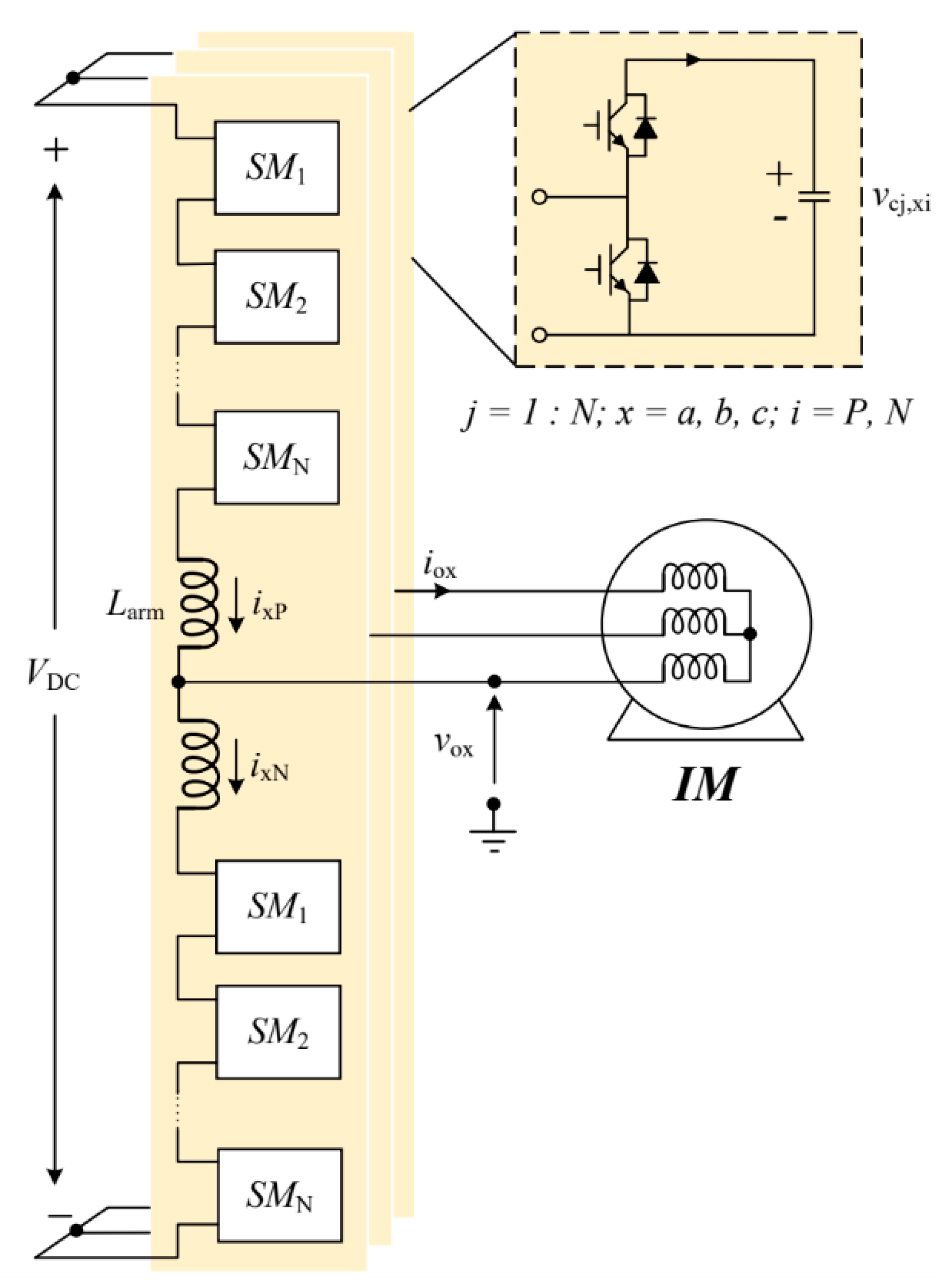
Figure 2.
The switching state of an HB-SM: (a) charged, (b) discharged, (c,d) bypassed.

Figure 3.
Procedure of estimating SM voltage fluctuation (Δvc,p−p).
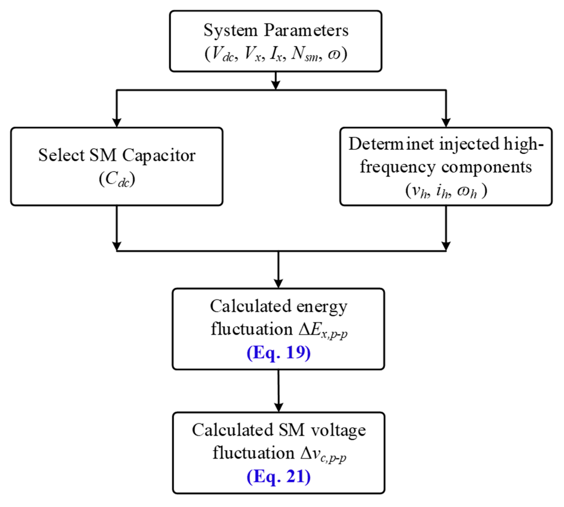
Figure 5.
Variation in SM capacitor voltage ripple (Δvp−p) as influenced by varying capacitance (Cdc) and operational frequency (fn).
Figure 5.
Variation in SM capacitor voltage ripple (Δvp−p) as influenced by varying capacitance (Cdc) and operational frequency (fn).

Figure 8.
Variation in SM capacitor voltage ripple (Δvc,p−p) based on injected high-frequency components and operating frequency (fn).
Figure 8.
Variation in SM capacitor voltage ripple (Δvc,p−p) based on injected high-frequency components and operating frequency (fn).

Figure 14.
The performance of the proposed voltage estimation algorithm: (a) SM capacitor voltage in the upper arm, (b) SM capacitor voltage in the lower arm.
Figure 14.
The performance of the proposed voltage estimation algorithm: (a) SM capacitor voltage in the upper arm, (b) SM capacitor voltage in the lower arm.

Figure 15.
Real-time performance of the proposed algorithm: (a) motor speed, (b) output current, (c) SM capacitor voltage.
Figure 15.
Real-time performance of the proposed algorithm: (a) motor speed, (b) output current, (c) SM capacitor voltage.
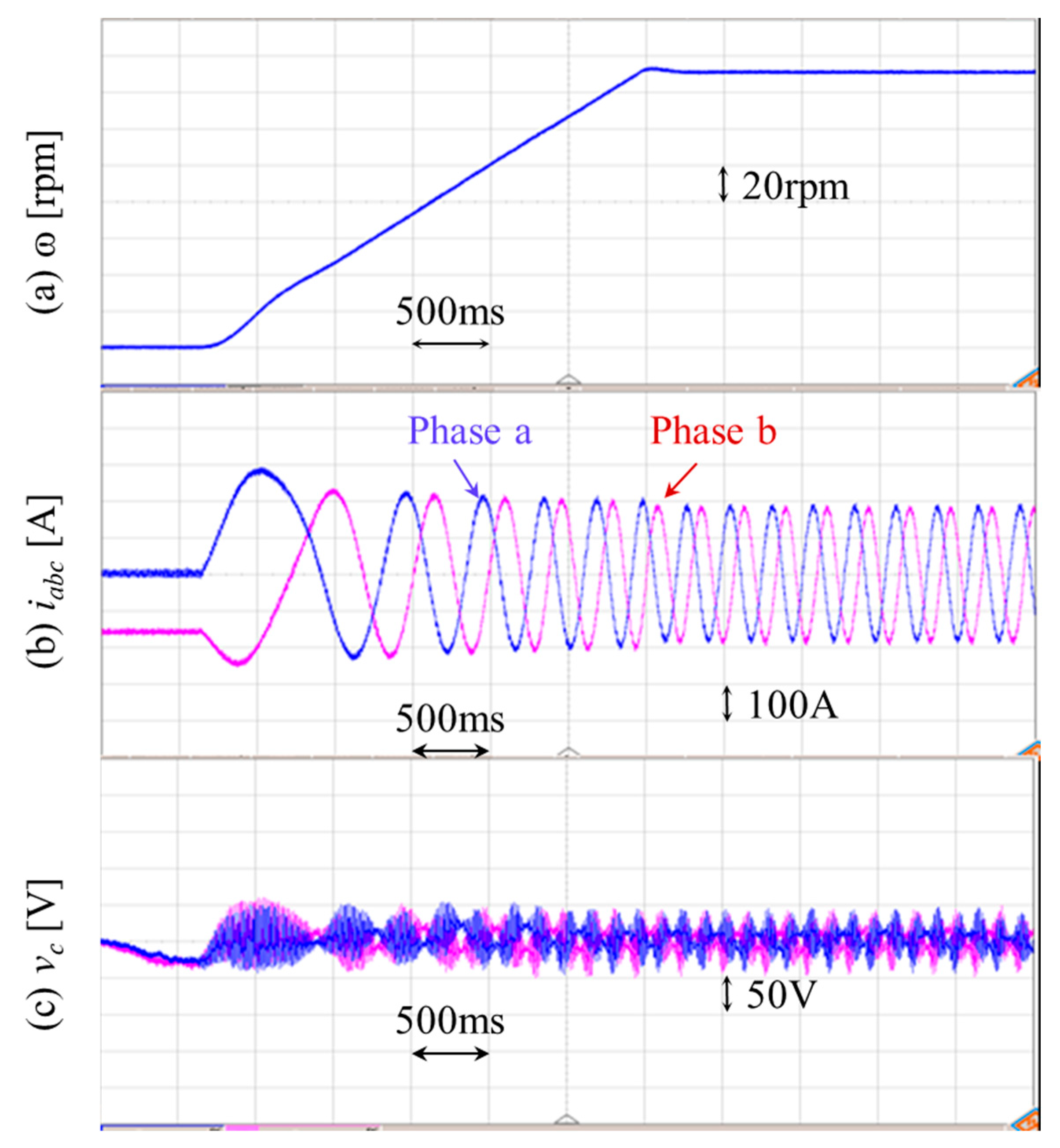
Table 1.
System Parameters.
| Parameters | Symbol | Values |
|---|---|---|
| DC-link voltage | VDC | 4800 V |
| Number of SMs per arm | NSM | 3 |
| Arm inductance | Larm | 1.5 mH |
| SM capacitance | Cdc | 1000 uF |
| Switching frequency | fsw | 2000 Hz |
| Nominal frequency | fn | 60 Hz |
| Rated voltage | Vrated | 3300 V |
| Rated current | Irated | 215 A |
| Rated speed | ωrated | 1800 rpm |
| Rated torque | Trated | 5306 N.m |
| Voltage ripple limit | Δvlim | 10% |
Disclaimer/Publisher’s Note: The statements, opinions and data contained in all publications are solely those of the individual author(s) and contributor(s) and not of MDPI and/or the editor(s). MDPI and/or the editor(s) disclaim responsibility for any injury to people or property resulting from any ideas, methods, instructions or products referred to in the content. |
© 2024 by the authors. Licensee MDPI, Basel, Switzerland. This article is an open access article distributed under the terms and conditions of the Creative Commons Attribution (CC BY) license (https://creativecommons.org/licenses/by/4.0/).
Share and Cite
MDPI and ACS Style
Nguyen, V.-T.; Kim, J.-W.; Lee, J.-W.; Park, B.-G. Optimal Design of a Submodule Capacitor in a Modular Multilevel Converter for Medium Voltage Motor Drives. Energies 2024, 17, 471. https://doi.org/10.3390/en17020471
AMA Style
Nguyen V-T, Kim J-W, Lee J-W, Park B-G. Optimal Design of a Submodule Capacitor in a Modular Multilevel Converter for Medium Voltage Motor Drives. Energies. 2024; 17(2):471. https://doi.org/10.3390/en17020471
Chicago/Turabian StyleNguyen, Van-Thang, Ji-Won Kim, Jae-Woon Lee, and Byoung-Gun Park. 2024. "Optimal Design of a Submodule Capacitor in a Modular Multilevel Converter for Medium Voltage Motor Drives" Energies 17, no. 2: 471. https://doi.org/10.3390/en17020471
Note that from the first issue of 2016, this journal uses article numbers instead of page numbers. See further details here.