Article

Fabrication and Characterization of Fullerene-Based Bulk Heterojunction Solar Cells with Porphyrin, CuInS2, Diamond and Exciton-Diffusion Blocking Layer

Department of Materials Science, The University of Shiga Prefecture, Hassaka 2500, Hikone, Shiga 522-8533, Japan
*
Author to whom correspondence should be addressed.
Energies 2010, 3(4), 671-685; https://doi.org/10.3390/en3040671
Submission received: 26 February 2010 / Accepted: 15 March 2010 / Published: 8 April 2010
(This article belongs to the Special Issue Solar Cells)

Abstract

:
Fullerene-based bulk heterojunction solar cells were fabricated, and the electronic and optical properties were investigated. C60 were used as n-type semiconductors, and porphyrin, CuInS2 and diamond were used as p-type semiconductors. An effect of exciton-diffusion blocking layer of perylene derivative on the solar cells between active layer and metal layer was also investigated. Optimized structures with the exciton-diffusion blocking layer improved conversion efficiencies. Electronic structures of the molecules were investigated by molecular orbital calculation, and energy levels of the solar cells were discussed. Nanostructures of the solar cells were investigated by transmission electron microscopy, electron diffraction and X-ray diffraction, which indicated formation of mixed nanocrystals.

1. Introduction

Carbon-based nanostructures such as fullerenes, nanocapsules, onions, nanopolyhedra, cones, cubes, and nanotubes have been widely reported and investigated [1,2,3,4]. These carbon (C) nanomaterials with hollow cage structures show different physical properties, and have the potential of studying materials of low dimensionality within an isolated environment. By controlling the size, layer numbers, helicity, compositions, and included clusters, the cluster-included C nanocage structures with band-gap energy of 0–1.7 eV and nonmagnetism are expected to show various electronic, optical, and magnetic properties such as Coulomb blockade, photoluminescence, and superparamagnetism [4,5].
Recently, C60-based polymer/fullerene solar cells have been investigated and reported [6,7,8,9]. These organic solar cells have a potential for use in lightweight, flexible, inexpensive and large-scale solar cells [10,11,12]. However, significant improvements of photovoltaic efficiencies are mandatory for use in future solar power plants. One of the improvements is donor-acceptor (DA) proximity in the devices by using blends of donor-like and acceptor-like molecules or polymers, which are called DA bulk-heterojunction solar cells [13,14,15].
The purpose of the present work is to fabricate and characterize C60-based bulk heterojunction solar cells. In the present work, 5,10,15,20-Tetraphenyl-21,23H-porphin zinc (ZnTPP), CuInS2 (CIS) and diamond was used for p-type semiconductors [9,16], and C60 with excellent electron affinity was used for n-type semiconductors. Porphyrin has high optical absorption in the visible spectrum and high hole mobility [17,18,19], and was expected to form cocrystallites with C60 [20,21] that would be suitable for the bulk heterojunction structure [22,23]. I-III-VI group compounds, called chalcopyrite, are expected as next generation solar cell materials, and CIS is one of the representative chalcopyrite compounds. Chalcopyrite compounds have advantages of high optical absorption and high resistivity to cosmic rays compared to conventional silicon solar cells [24,25]. In addition, they have a band structure of direct transition, which shows high quantum efficiency.
The second purpose is to investigate an effect of exciton-diffusion blocking layer (EBL). 3,4,9,10-perylenetetracarboxylic dianhydride (PTCDA) is a perylene derivative with a simple structure, which was reported to be used for solar cells [26]. In the present work, PTCDA was used as the EBL for ZnTPP:C60 bulk heterojunction solar cells. EBL prevents hole transfer between active layer and anode, and improvement of conversion efficiency was expected by an introduction of the EBL. Device structures were produced, and efficiencies and optical absorption were investigated. The present work will indicate a guideline for new-type organic-inorganic solar cells using C60.

2. Experimental Procedures

A schematic diagram of the present C60-based bulk heterojunction solar cells is shown in Figure 1. A thin layer of polyethylenedioxythiophen doped with polystyrene-sulfonic acid (PEDOT:PSS) (Sigma Aldrich) was spin-coated on pre-cleaned indium tin oxide (ITO) glass plates (Geomatec Co., Ltd., ~10 Ω/□). The PEDOT:PSS has a role as an electron blocking layer for hole transport. Then, semiconductor layers were prepared on a PEDOT layer by spin coating using a mixed solution of C60 (Material Technologies Research Ltd., 99.98%), ZnTPP (Sigma Aldrich) in 1 mL o-dichlorobenzene (Nacalai Tesque, Inc., 99%). Total weight of ZnTPP:C60 was 18 mg, and weight ratio of ZnTPP:C60 was 3:7.
CIS solution for p-type semiconductors were produced by dissolving CuI (Sigma Aldrich Corp., 99.99%) and InCl3 (Sigma Aldrich Corp., 99.99%) in a mixture of triphenylphosphite (1 mL) (Sigma Aldrich Corp., 97%) and acetonitrile (2 mL) (Nacalai Tesque, Inc., 99.5%), dropping bis(trimethylsilyl)sulfide (Tokyo Chemical Industry Co., Ltd., >95%) [27,28]. The solution for n-type semiconductors was prepared by dissolving C60 in o-dichlorobenzene. A thin layer of polyethylenedioxythiophene doped with polystyrene-sulfuric acid (PEDOT:PSS) (Sigma Aldrich) was spin-coated on a pre-cleaned fluorine dope tin oxide (FTO) glass plates (Asahi Glass, ~9.3 Ω/□). Then, semiconductor layers were prepared on a PEDOT:PSS layer by spin coating, and annealed at 120 ºC for 10 min in N2 atmosphere. The FTO was used because of the high temperature annealing process.
The thickness of the blended device was ~150 nm. To increase efficiencies, PTCDA with a thickness of ~20 nm was also added over the active layers as shown in Figure 1. After annealing at 100 °C for 30 min in N2 atmosphere, PTCDA (Wako Pure Chemical Industries Ltd.) was evaporated between active layer and metal layer. Finally, aluminum (Al) metal contacts were evaporated as a top electrode, and annealed at 140 °C for 20 min in N2 atmosphere.
Current density-voltage (J-V) characteristics (Hokuto Denko Corp., HSV-100) of the solar cells were measured both in the dark and under illumination at 100mW/cm2 by using an AM 1.5 solar simulator (San-ei Electric, XES-301S) in N2 atmosphere. The solar cells were illuminated through the side of the ITO substrates, and the illuminated area is 0.16 cm2. Optical absorption of the solar cells was investigated by means of UV-visible spectroscopy (Hitachi U-4100). Transmission electron microscope (TEM) observation was carried out by a 200 kV TEM (Hitachi H-8100). The microstructures were also investigated by X-ray diffraction (XRD, Philips X’ Pert-MPD System).
The isolated molecular structures were optimized by ab-initio molecular orbital calculations using Gaussian 03. Conditions in the present calculation were as follows: calculation type (FOPT), calculation method (RHF) and basis set (6-31G). Electronic structures such as energy gaps between highest occupied molecular orbital (HOMO) and lowest unoccupied molecular orbital (LUMO), and electron densities were investigated.
Figure 1. Structure of C60-based bulk heterojunction solar cells with PTCDA layer.
Energies 03 00671 g001

3. Results and Discussion

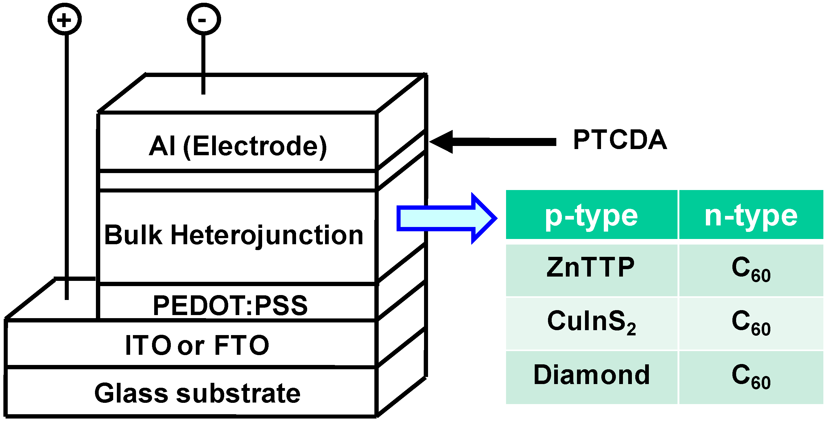
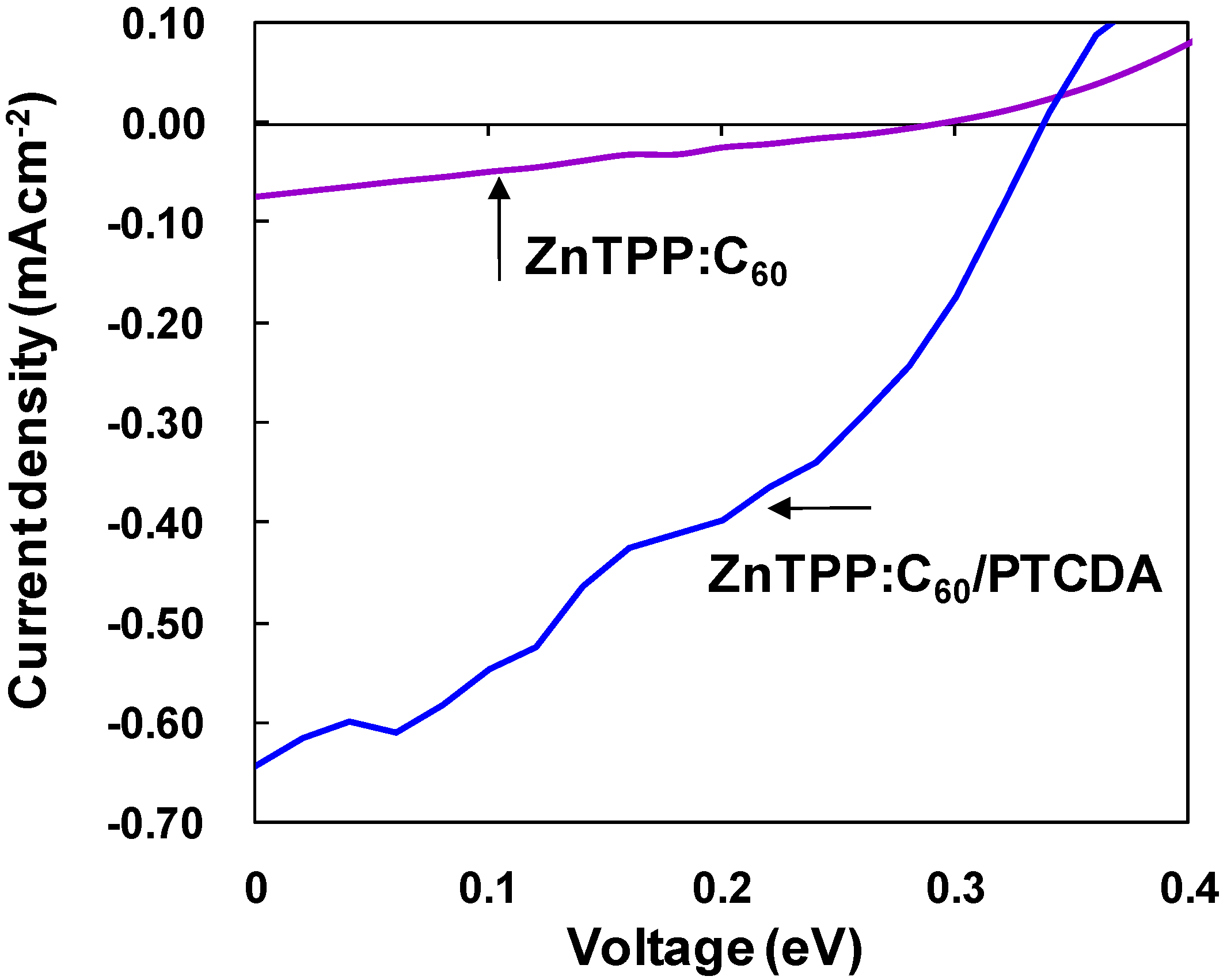
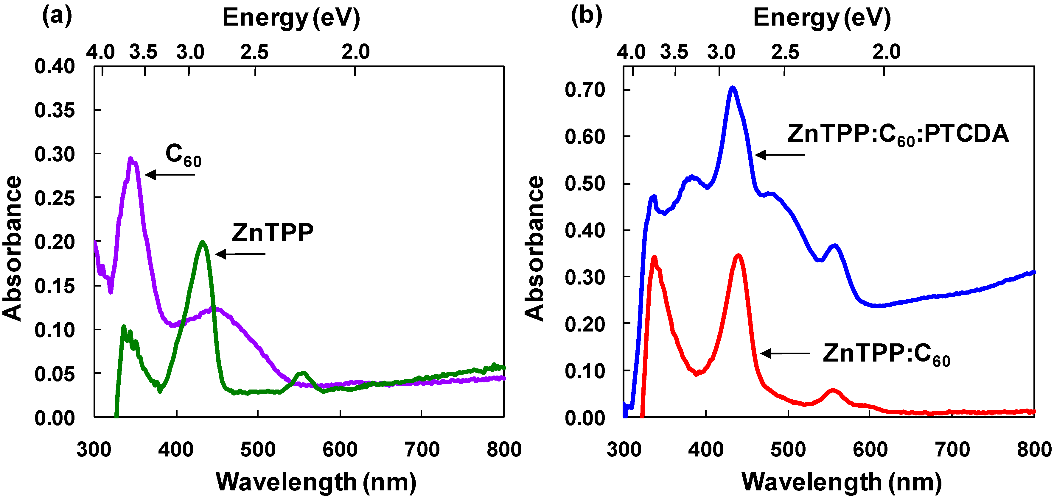
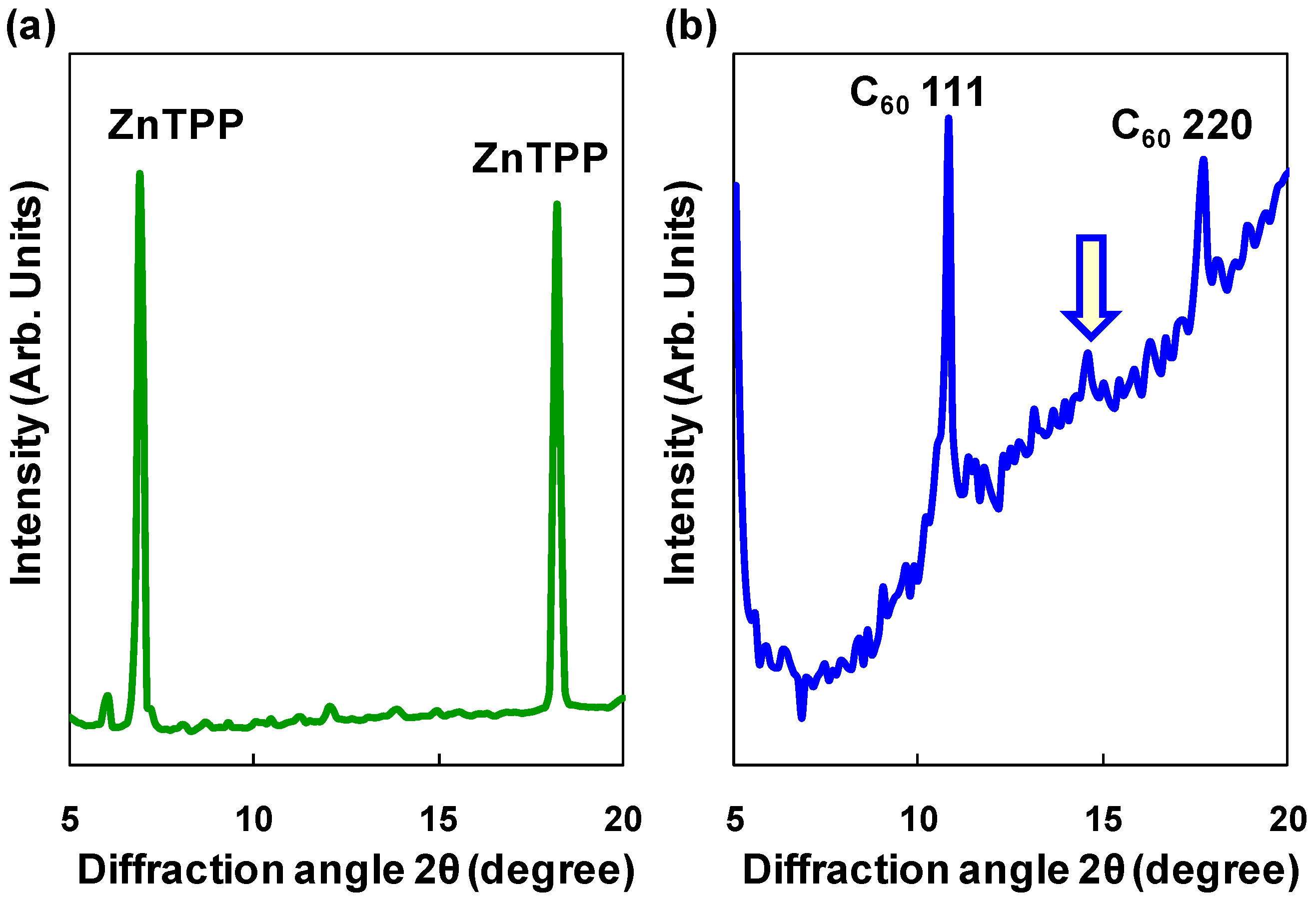
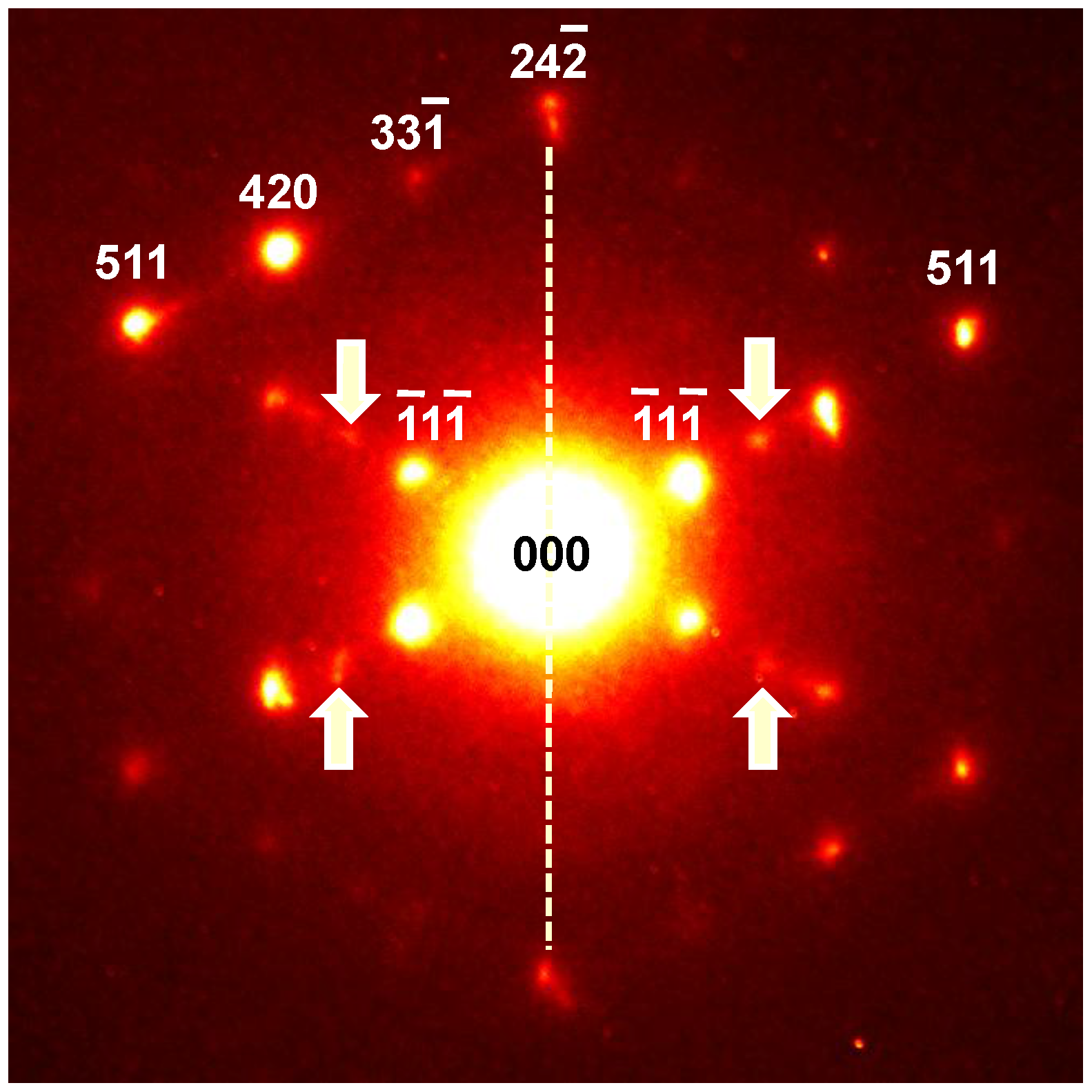
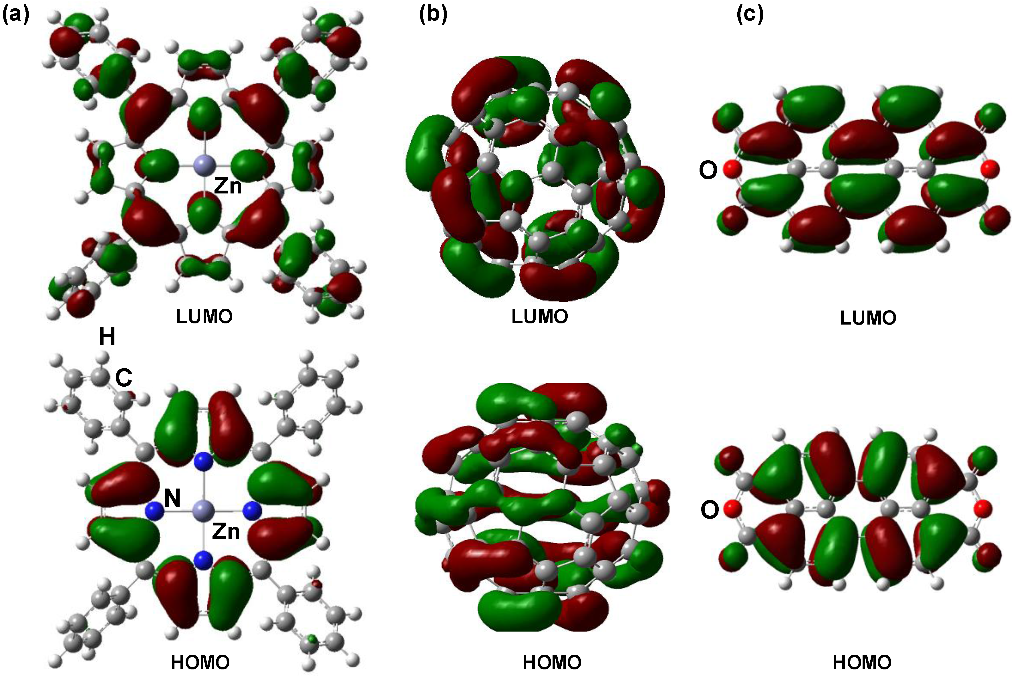
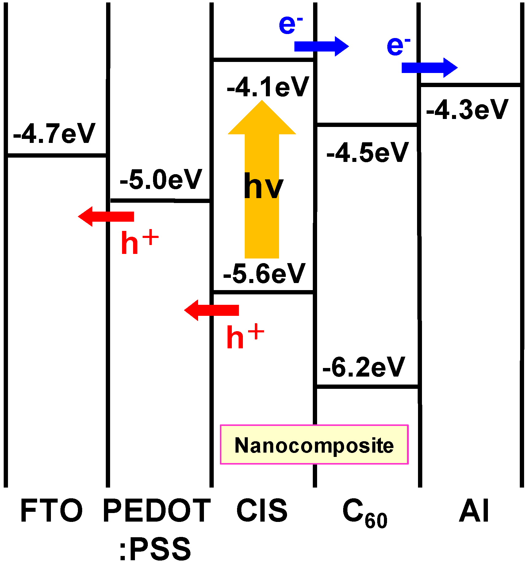
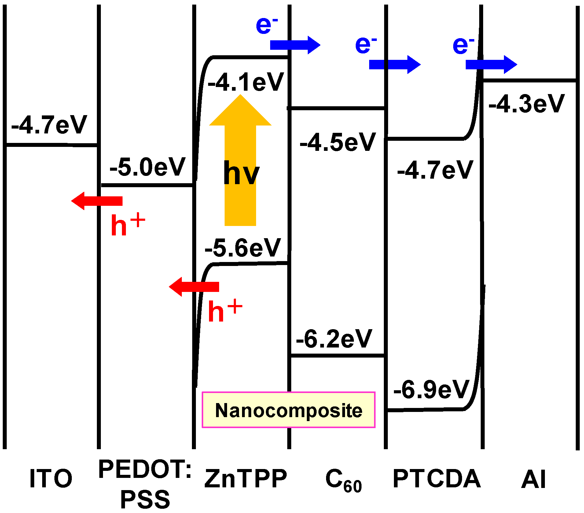
3.1. ZnTPP:C60 bulk heterojunction solar cells

Measured J-V characteristic of ZnTPP:C60 bulk heterojunction solar cells under illumination is shown in Figure 2. The bulk heterojunction indicates a one layered composite structures with p- and n-type semiconductors, which is denoted as ZnTPP:C60. Effects of PTCDA addition to the ZnTPP:C60 bulk heterojunction solar cells were also investigated, which is denoted as ZnTPP:C60/PTCDA. Each structure shows a characteristic curve for open circuit voltage and short circuit current density, and measured parameters of the present solar cells are summarized in Table 1. Power conversion efficiency, fill factor, short-circuit current density and open-circuit voltage are denoted as η, FF, JSC, and VOC, respectively. As shown in Figure 2 and Table 1, current density of ZnTPP:C60 increased by PTCDA addition, and the best efficiency was obtained for the ZnTPP:C60/PTCDA sample.
Figure 2. Measured J-V characteristic of ZnTPP:C60 bulkheterojunction solar cells under illumination.
Energies 03 00671 g002
Table 1. Measured parameters of the present solar cells.
SampleVOC (V)JSC (mAcm−2)FFη (%)
ZnTTP:C60/PTCDA0.330.620.387.8 × 10−2
ZnTTP:C600.300.0740.265.8 × 10−3
CuInS2:C600.180.0160.288.0 × 10−4
Diamond:C600.0230.00530.354.3 × 10−5
Figure 3 shows the optical absorption of C60, ZnTPP, ZnTPP:C60 and ZnTPP:C60/PTCDA bulk heterojunction solar cells. The ZnTPP:C60/PTCDA structure provided higher photo-absorption in the range of 300 to 800 nm (which correspond to 4.0 and 1.5 eV, respectively), compared to the ZnTPP:C60 structure. Exciton migration of C60 can be efficiently suppressed by use of PTCDA [21], and exciton would be generated for both ZnTPP/C60 and C60/PTCDA interfaces, which results in the increase of conversion efficiency, as listed in Table 1.
X-ray diffraction patterns of ZnTPP and ZnTPP:C60 bulk heterojunction layers are shown in Figure 4(a) and Figure 4(b), respectively. In Figure 4(a), diffraction peaks corresponding to ZnTPP crystal are observed. After formation of ZnTPP:C60 bulk heterojunction layer, the diffraction peaks corresponding to ZnTPP disappeared, and C60 peaks are observed as shown in Figure 4(b). In addition, a new diffraction peak is observed as indicated by an arrow, which would be believed to be porphyrin/C60 cocrystallites [20,21].
Figure 3. Absorbance spectrum of (a) C60, ZnTPP and (b) ZnTPP:C60 bulk heterojunction solar cells.
Energies 03 00671 g003
Figure 4. X-ray diffraction pattern of (a) ZnTPP and (b) ZnTPP:C60 bulk heterojunction layer.
Energies 03 00671 g004
Figure 5 is an electron diffraction pattern of ZnTPP:C60 bulk heterojunction layer, taken along the [-123] direction of C60. A twin structure with the (112) twin plane is observed in Figure 5, as indicated by a dotted line. Diffraction spots which would correspond to cocrystallites of ZnTPP:C60 are also observed as indicated by arrows.
Electronic structures of the molecules were calculated, and energy levels of highest occupied molecular orbital (HOMO) and lowest unoccupied molecular orbital (LUMO) are shown in Figure 6. HOMO levels in Figure 6(a), electrons are localized around the pyrrole rings of the ZnTPP. Energy levels of LUMO of C60 and PTCDA are also shown in Figure 6(b,c), respectively. The separated carriers would transfer from ZnTPP to C60, and from ZnTPP/C60 to PTCDA.
Figure 5. Electron diffraction pattern of ZnTPP:C60 bulk heterojunction layer.
Energies 03 00671 g005
Figure 6. Calculated LUMO and HOMO levels of (a) ZnTPP (b) C60 and (c) PTCDA.
Energies 03 00671 g006
An energy level diagram of the ZnTPP/C60/PTCDA solar cell is summarized in Figure 7. Previously reported values [7,8] were used for the energy levels of the figures by adjusting to the present work. The incident direction of light is from the ITO side. Energy barrier would exist near the semiconductor/metal interface. Electronic charge-transfer separation was caused by light irradiation from the ITO substrate side. Electrons are transported to an Al electrode, and holes are transported to an ITO substrate. The VOC of organic solar cells is reported to be determined by the energy gap between HOMO of donor molecule and LUMO of accepter molecule, and a relation between VOC and polymer oxidation potential is VOC = (1/e)(|EZnTPPHOMO| – |EC60LUMO|) – 0.3 (V), where e is the elementary charge [29]. The value of 0.3 V is an empirical factor, and this is enough for efficient charge separation [30]. The present experimental data of VOC indicated smaller compared to the calculated ones from the equation, which might be due to the voltage descent at the metal/semiconductor interface, and control of the energy levels is also important to increase the efficiency.
Figure 7. Energy level diagram of ZnTPP/C60/PTCDA solar cell.
Energies 03 00671 g007
In the present work, efficiencies of the solar cells were increased by addition of PTCDA layers, which would work as the exciton-diffusion blocking layer for porphyrin:C60 bulk heterojunction solar cells. The PTCDA layers prevents hole transfer between the porphyrin:C60 active layer and aluminum, and the conversion efficiencies were improved.
Since the microstructure of ZnTPP and C60 bulk heterojunction layer is strongly dependent on the weight ratio of these, it is necessary to control the microstructure to form cocrystallites of ZnTPP:C60. In the present work, higher efficiencies were obtained for the ZnTPP:C60 sample with the weight ratio of 3:7, which would be suitable for the cocrystallite formation, as observed for weak reflections in X-ray and electron diffraction patterns. Recombination of electrons of C60 and holes of ZnTPP would occur in the bulk heterojunction layer with intermittent cocrystallite structure. If continuous cocrystallite structures form perpendicular to the thin films, it is believed that the recombination of electrons and holes could be suppressed, which would lead to improvement of conversion efficiency.

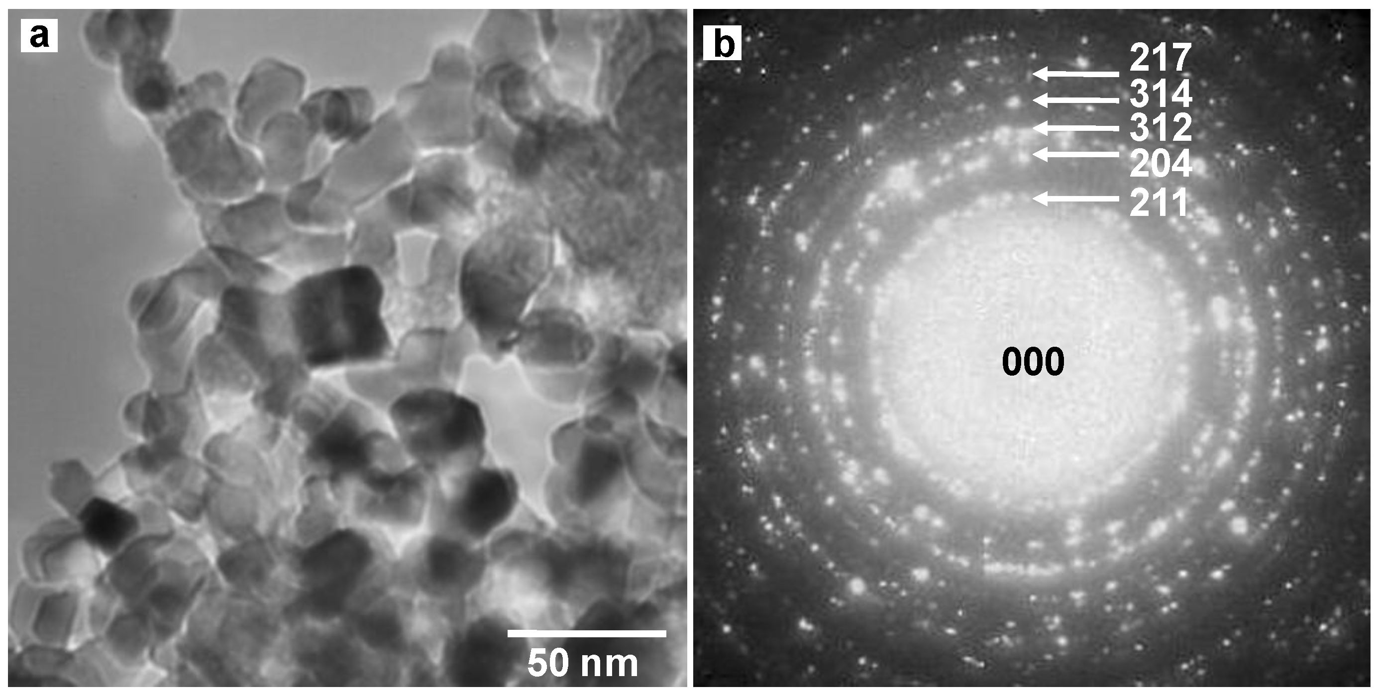
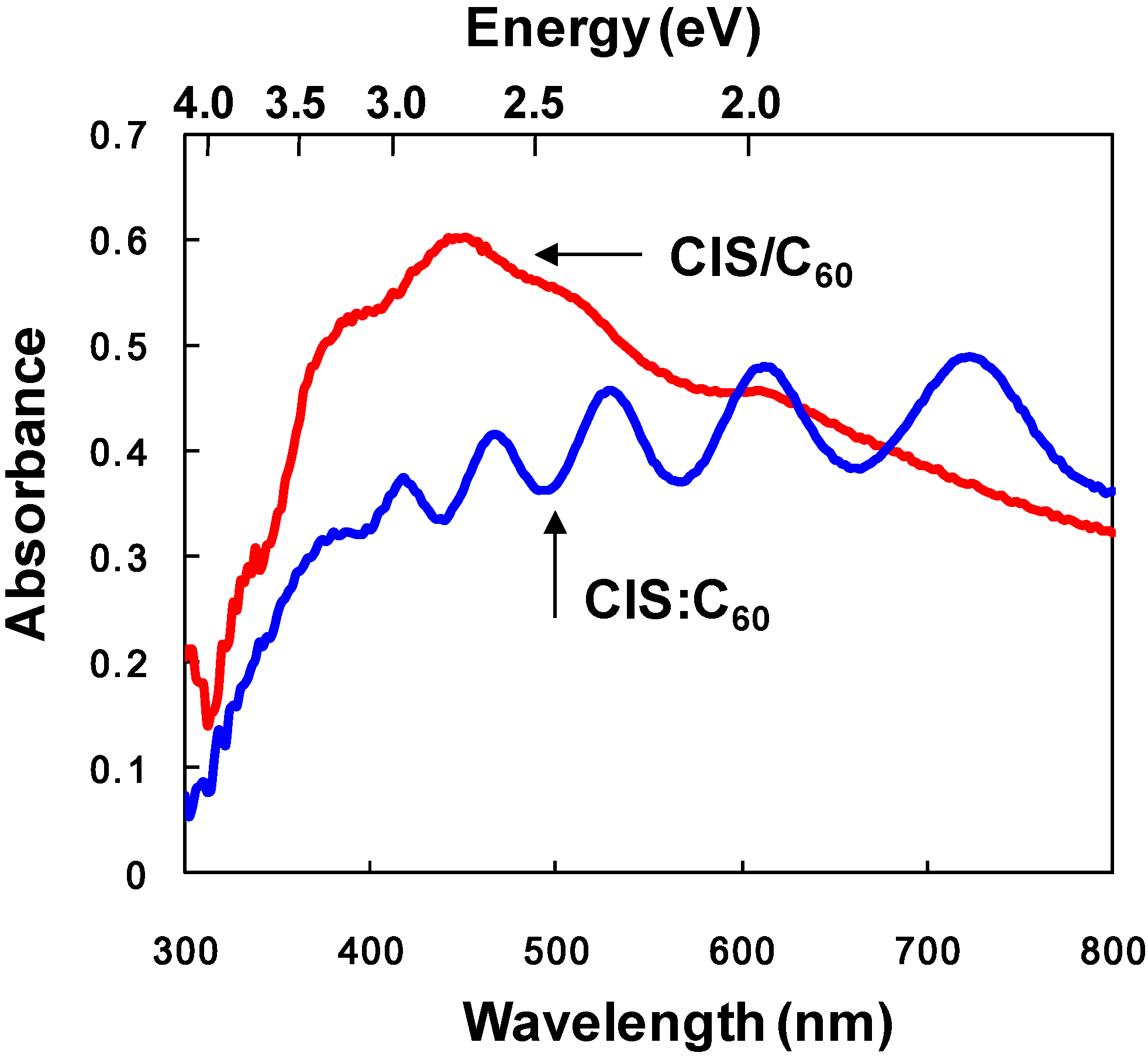
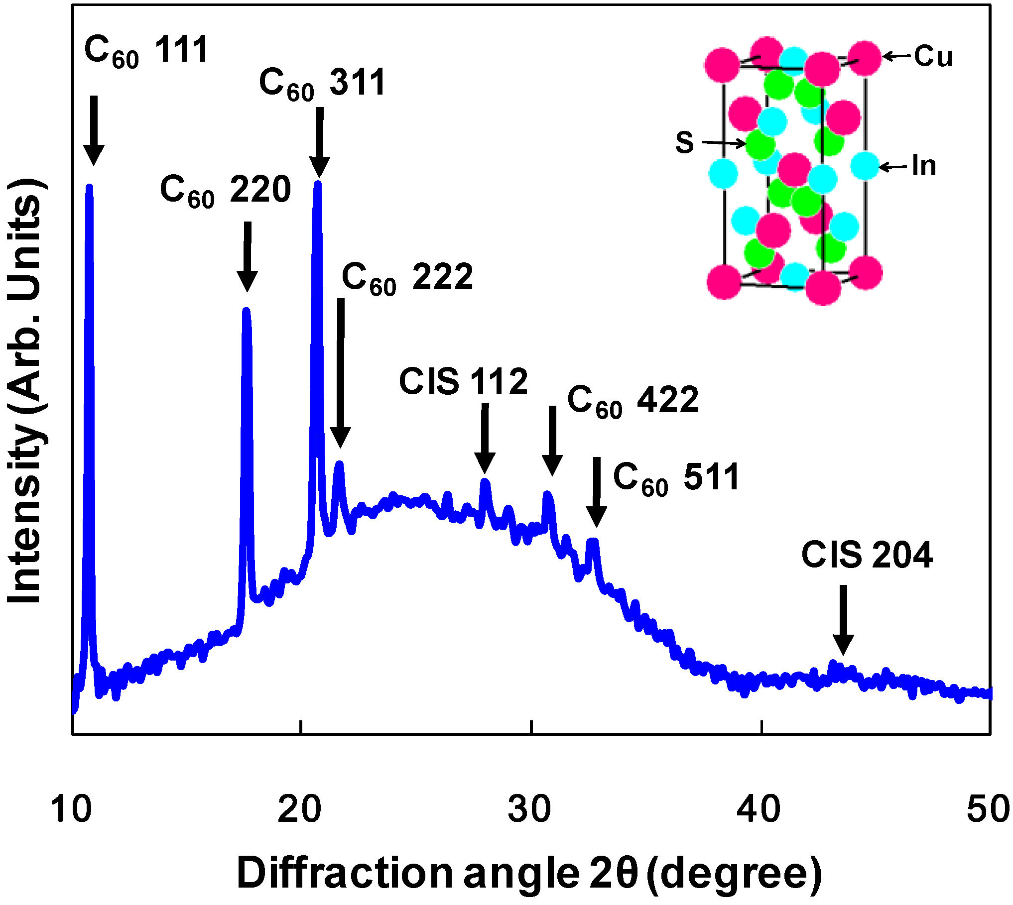
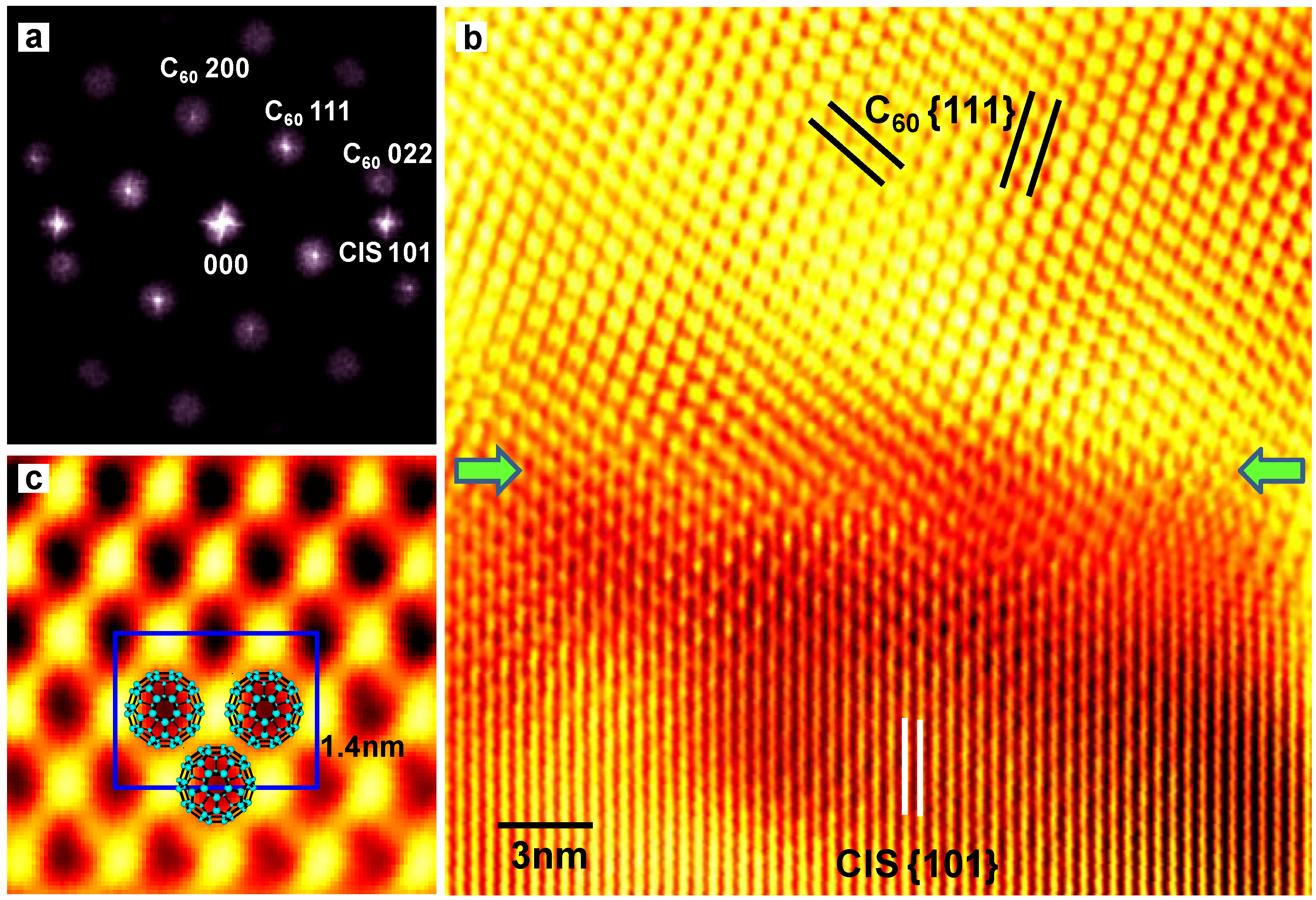
3.2. CuInS2:C60 bulk heterojunction solar cells

Measured parameters of a CuInS2:C60 bulk heterojunction structure are summarized in Table 1. A solar cell with CIS:C60 bulk heterojunction structure provided power convergent efficiency of 8.0 × 10⁻⁴%, fill factor of 0.28 and open-circuit voltage of 0.18 V. The p-n interfaces, which are photoelectron conversion areas were increased by using blend structures of p-type and n-type semiconductors.
Figure 8 shows a measured optical absorption of the solar cells based on CIS. These solar cells show a wide optical absorption range from 400 to 800 nm, and the heterojunction solar cell show as higher optical absorption range from 350 nm to 550 nm than that of the bulk heterojunction. Since the FTO substrate was set as an incident side, the optical absorption of the CIS layer was high for the heterojunction structure. On the other hand, optical absorption of the bulk heterojunction would be lower compared to that of the heterojunction structure because C60 were mixed with the CIS layer.
Figure 8. Optical absorption spectra of heterojunction and bulk heterojunction solar cells.
Energies 03 00671 g008
An X-ray diffraction pattern of CIS:C60 bulk heterojunction is shown in Figure 9. Several diffraction peaks are observed, which correspond to 112, 204 of CIS and 111, 220, 311, 222, 422, 511 of C60. The average particle sizes of CuInS2 and C60 were calculated from Scherrer’s formula to be 5 nm and 13 nm, respectively. The 204 peak of CIS is too small to be used for the calculation of the CIS grain size, and only one peak of 112 was used for the calculation.
Figure 9. X-ray diffraction pattern of CIS:C60 thin film.
Energies 03 00671 g009
Figure 10(a) is a TEM image of CIS, and many CIS particles are observed. Figure 10(b) is an electron diffraction pattern of CIS. Debye-Scherrer rings are observed in the diffraction pattern, which shows crystallite structures of CIS particles.
Figure 10. X-ray diffraction pattern of CIS:C60 thin film.
Energies 03 00671 g010
An interfacial structure of CIS and C60 was observed by TEM as shown in Figure 11. Filtered Fourier transform of the HREM image of CIS:C60 bulk heterojunction layer is shown in Figure 11(a). Figure 11(b) is an inverse Fourier transform of (a), and arrows show the interface of CIS and C60. Lattice fringes of {101} of CIS and {111} of C60 were observed. The enlarged image of a part of C60 in (b) is shown in Fig 11(c). Arrangements of C60 molecules are observed in the image. CIS and C60 have size distribution, and the crystal sizes of them observed in the TEM image are larger compared to the averaged sizes.
Figure 11. (a) Filtered Fourier transform of HREM image of CIS:C60 bulk heterojunction layer. (b) Inverse Fourier transform of (a). (c) Enlarged image of a part of C60 in (b).
Energies 03 00671 g011
Optimization of the nanocomposite structure with CIS and C60 would increase the efficiencies of the bulk heterojunction solar cell. From the present TEM observation, CIS and C60 were not mixed in a molecular scale. If the mixture structure of CIS and C60 is improved to a nanoscale, it is believed that the area of the p-n junction interfaces is increased, and the efficiency would be improved. In addition, it is important to search the most suitable mixture ratio of the p-type and n-type semiconductors for bulk heterojunction solar cells.
An energy level diagram of CIS/C60 solar cells is summarized as shown in Figure 12. Previously reported values were used for the energy levels of the figures by adjusting them to the present work [15,26,31]. When light is incident from the FTO side, excitation by the light absorption happens in the p-n interface, and electrons and holes are produced by charge separation. Carriers would transport from –4.5 eV to –4.3 eV by hopping conduction. Improvement of the present bulk heterojunction solar cells would be possible by the introduction of a buffer layer, change of annealing conditions, and the improvement of the microstructure is also necessary to obtain high efficiency.
Figure 12. Energy level diagram of CIS:C60 solar cell.
Energies 03 00671 g012
The evaporation method provided high quality thin films, but a high vacuum and high temperature process are necessary. Although CISCuT method is a productive process, it requires a high temperature process [32]. On the other hand, the present spin coating method is simpler compared to the other formation methods. In addition, we can apply the spin coating method to plastic substrates without high vacuum and high temperature processes.

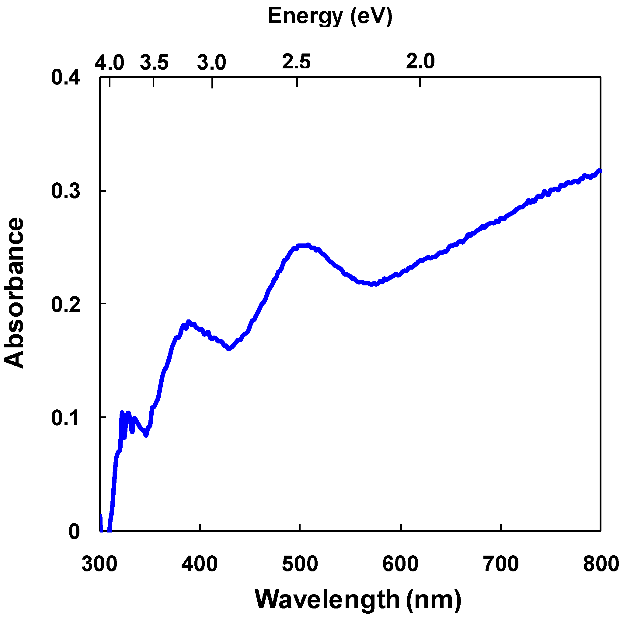
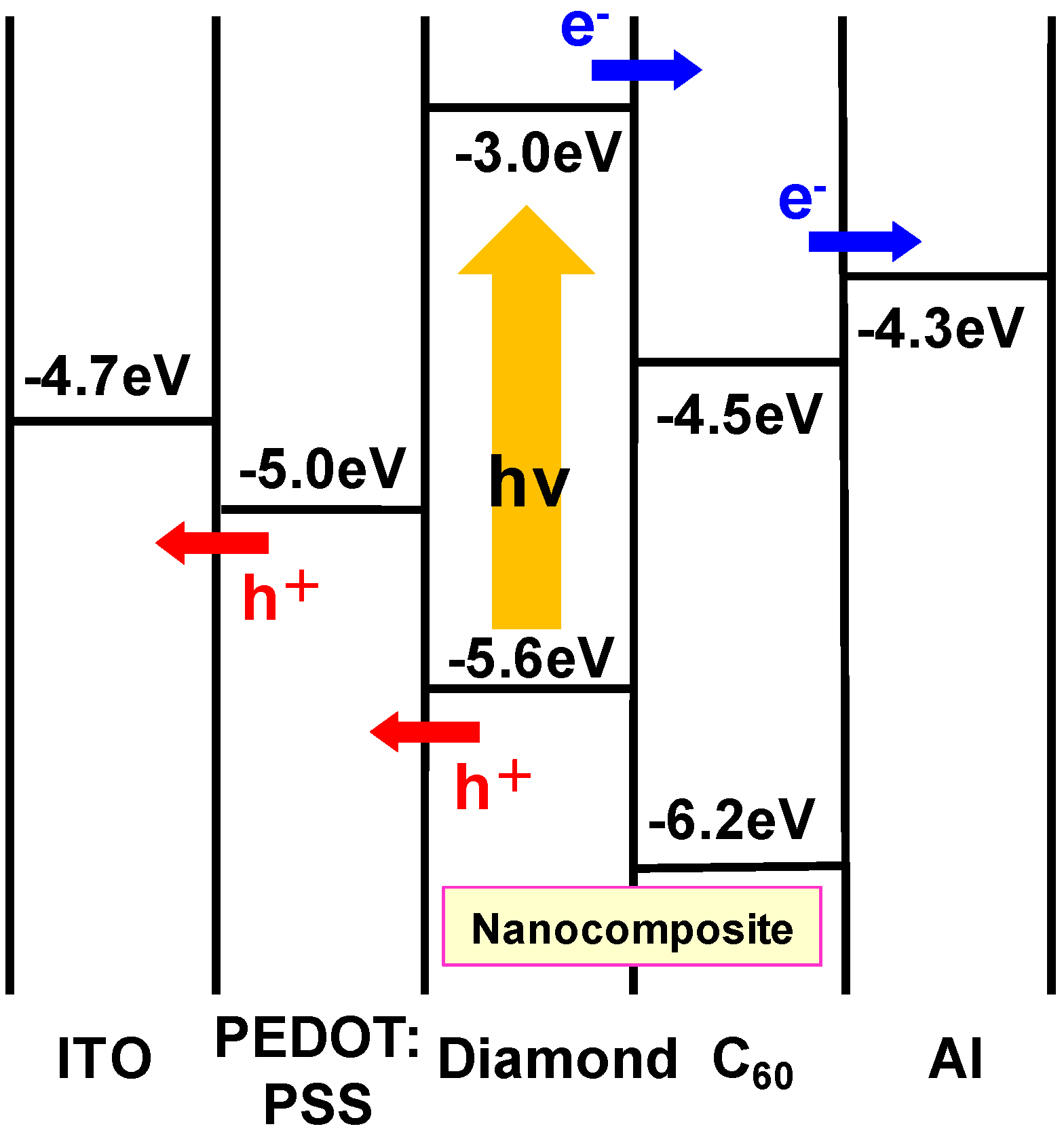
3.3. Diamond:C60 bulk heterojunction solar cells

Measured J-V characteristic of diamond:C60 bulk heterojunction solar cell under illumination showed characteristic curve for open circuit voltage and short circuit current. A solar cell with the diamond:C60 structure provided power convergent efficiency of 4.3 × 10⁻⁵%, fill factor of 0.35, short circuit current of 5.3 μA/cm2 and open circuit voltage of 0.023 V, as listed in Table 1.
Figure 13 shows optical absorption of the diamond:C60 bulk heterojunction solar cell. The diamond:C60 bulk heterojunction structure provided photo-absorption in the range of 350 to 500 nm, and shows high absorption at 339, 402 and 506 nm, which correspond to 3.7, 3.1 and 2.5 eV, respectively. Absorption peaks of the C60 were confirmed within the range from 300 to 400 nm, and an absorption peak of 506 nm corresponds to the diamond.
Figure 13. Optical absorption spectrum of diamond:C60 bulk heterojunction solar cell.
Energies 03 00671 g013
X-ray diffraction pattern of diamond powder showed diffraction peaks of diamond powder, which were confirmed as 111, 220 and 311 of the diamond structure. A grain size of diamond powder was determined to be 12 nm, which was calculated by Scherrer’s equation. An increase of photo-absorption under the long wavelength would be due to the nanostructure of nanodiamond particles, which will be discussed later.
An energy level diagram of diamond:C60 solar cell is summarized as shown in Figure 14. Previously reported values were also used for the energy levels [15]. An energy gap of diamond estimated from Figure 13, which corresponds to absorbance of 506nm, is used for the model. From a theoretical calculation [33], nanodiamonds are composed of three layers; a diamond core (sp3), a middle core (sp2+x) and a graphitized core (sp2). Therefore, a band gap of the nanodiamond is decreased by the existence of the sp2+x bonding [34,35]. The carrier transport mechanism is considered as follows; when light is incident from the ITO substrate, light absorption excitation occurs at the p-n heterojunction interface, and electrons and holes appear by charge separation. Then, the electrons transport through C60 toward the Al electrode, and the holes transport through PEDOT:PSS to the ITO substrate. Since it has been reported that Voc is nearly proportional to band gaps of semiconductors [36], control of energy levels is important to increase the efficiency. The low cell performance would be due to the insufficient dispersion of diamond and C60 in the composite layer, and further control of the nanocrystals is needed.
Figure 14. Energy level diagram of diamond:C60 bulk heterojunction solar cell.
Energies 03 00671 g014
An advantage for the bulk heterojunction structure is increased p-n heterojunction interface. However, due to disarray of the diamond:C60 microstructure, electrons and holes could not transport smoothly by carrier recombination at the C60/Al interface, and at the PEDOT:PSS/diamond interface, respectively. To solve these problems, introduction of a layer preventing carrier recombination and improvement of crystalline structure with few defects are needed.
In the present work, an organic-inorganic hybrid solar cell was fabricated and characterized. For the carbon-based solar cells in previous works, thin films are fabricated by a CVD method. In the present work, solar cells with C60 as an organic semiconductor and diamond as an inorganic semiconductor were fabricated by a spin coating method, which is a low cost method. Boron nitride acts as p-type semiconductor, and diamond has a similar crystal structure as boron nitride. Combination of the present solar cells and nanomaterials such as diamond or boron nitride with various direct band gaps might be effective for increase of efficiencies [37]. The performance of the present solar cells would be dependent on the nanoscale structures of the organic-inorganic materials, and control of the structure should be investigated further.

4. Conclusions

C60-based bulk heterojunction solar cells were fabricated and characterized. A device based on ZnTPP:C60/PTCDA provided η of 7.8 × 10⁻²%, FF of 0.38, JSC of 0.62 mA/cm2 and VOC of 0.33 V. Conversion efficiency was increased by introduction of PTCDA layer because the exciton migration of C60 can be efficiently suppressed by use of PTCDA. A device of bulk heterojunction structure based on CuInS2:C60 and diamond:C60 were also fabricated and characterized. Photovoltaic behavior including charge transfer and mobility can be described on the basis of the energy diagram of the bulk heterojunction solar cells from the present J-V measurements, optical absorption and structure analysis. Optimization of blended structures with C60 would increase the efficiencies of solar cells.

Acknowledgements

The authors would like to thank R. Motoyoshi, K. Nomura, N. Kakuta, A. Kawashima, S. Kikuchi and S. Yoshida for experimental help and useful advices.

References

  1. Kroto, H.W.; Heath, J.R.; O’Brien, S.C.; Curl, R.F.; Smalley, R.E. C60: Buckminsterfullerene. Nature 1985, 318, 162–163. [Google Scholar] [CrossRef]
  2. Iijima, S. Helical microtubules of graphitic carbon. Nature 1991, 354, 56–58. [Google Scholar] [CrossRef]
  3. Oku, T.; Narita, I.; Nishiwaki, A.; Koi, N.; Suganuma, K.; Hatakeyama, R.; Hirata, T.; Tokoro, H.; Fujii, S. Formation, atomic structures and properties of carbon nanocage materials. Topics Appl. Phys. 2006, 100, 187–216. [Google Scholar]
  4. Oku, T.; Hirano, T.; Kuno, M.; Kusunose, T.; Niihara, K.; Suganuma, K. Synthesis, atomic structures and properties of carbon and boron nitride fullerene materials. Mater. Sci. Eng. B 2000, 74, 206–217. [Google Scholar] [CrossRef]
  5. Oku, T.; Kuno, M.; Kitahara, H.; Narita, I. Formation, atomic structures and properties of boron nitride and carbon nanocage fullerene materials. Int. J. Inorg. Mater. 2001, 3, 597–612. [Google Scholar] [CrossRef]
  6. Sariciftci, N.S.; Smilowitz, L.; Heeger, A.J.; Wudl, F. Photoinduced electron transfer from a conducting polymer to Buckminsterfullerene. Science 1992, 258, 1474–1476. [Google Scholar] [CrossRef] [PubMed]
  7. Hayashi, Y.; Yamada, I.; Takagi, S.; Takasu, A.; Soga, T.; Jimbo, T. Influence of structure and C60 composition on properties of blends and bilayers of organic donor-acceptor polymer/C60 photovoltaic devices. Jpn. J. Appl. Phys. 2005, 44, 1296–1300. [Google Scholar] [CrossRef]
  8. Oku, T.; Nagaoka, S.; Suzukia, A.; Kikuchi, K.; Hayashi, Y.; Inukai, H.; Sakuragi, H.; Soga, T. Formation and characterization of polymer/fullerene bulk heterojunction solar cells. J. Phys. Chem. Solids 2008, 69, 1276–1279. [Google Scholar] [CrossRef]
  9. Oku, T.; Noma, T.; Suzuki, A.; Kikuchi, K.; Kikuchi, S. Fabrication and characterization of fullerene/porphyrin bulk heterojunction solar cells. J. Phys. Chem. Solids 2009, (in press). [Google Scholar]
  10. Ma, W.; Yang, C.; Gong, X.; Lee, K.; Heeger, A.J. Thermally stable, efficient polymer solar cells with nanoscale control of the interpenetrating network morphology. Adv. Funct. Mater. 2005, 15, 1617–1622. [Google Scholar] [CrossRef]
  11. Granström, M.; Petritsch, K.; Arias, A.C.; Lux, A.; Andersson, M.R.; Friend, R.H. Laminated fabrication of polymeric photovoltaic diodes. Nature 1998, 395, 257–260. [Google Scholar] [CrossRef]
  12. Oku, T.; Nagaoka, S.; Suzuki, A.; Kikuchi, K.; Hayashi, Y.; Sakuragi, H.; Soga, T. Formation and characterization of MEH-PPV/PCBM-based bulk heterojunction solar cells. J. Ceramic Processing Res. 2008, 9, 549–552. [Google Scholar]
  13. Yu, G.; Heeger, A.J. Charge separation and photovoltaic conversion in polymer composites with internal donor/acceptor heterojunctions. J. Appl. Phys. 1995, 78, 4510–4515. [Google Scholar] [CrossRef]
  14. Padinger, F.; Rittberger, R.S.; Sariciftci, N.S. Effects of postproduction treatment on plastic solar cells. Adv. Funct. Mater. 2003, 13, 85–88. [Google Scholar] [CrossRef]
  15. Oku, T.; Kakuta, N.; Kawashima, A.; Nomura, K.; Motoyoshi, R.; Suzuki, A.; Kikuchi, K.; Kinoshita, G. Formation and characterization of bulk hetero-junction solar cells using C60 and perylene. Mater. Trans. 2008, 49, 2457–2460. [Google Scholar] [CrossRef]
  16. Takahashi, K.; Kuraya, N.; Yamaguchi, T.; Komura, T.; Murata, K. Three-layer organic solar cell with high-power conversion efficiency of 3.5%. Solar Energy Mater. Solar Cells 2000, 61, 403–416. [Google Scholar] [CrossRef]
  17. Hasobe, T.; Imahori, H.; Kamat, P.V.; Ahn, T.K.; Kim, S.K.; Kim, D.; Fujimoto, A.; Hirakawa, T.; Fukuzumi, S. Photovoltaic cells using composite nanoclusters of porphyrins and fullerenes with gold nanoparticles. J. Am. Chem. Soc. 2005, 127, 1216–1228. [Google Scholar] [CrossRef] [PubMed]
  18. Sun, Q.; Dai, L.; Zhou, X.; Li, L.; Li, Q. Bilayer- and bulk-heterojunction solar cells using liquid crystalline porphyrins as donors by solution processing. Appl. Phys. Lett. 2007, 91, 253505-1-3. [Google Scholar] [CrossRef]
  19. Hasobe, T.; Sandanayaka, A.S.; Wada, T.; Araki, Y. Fullerene-encapsulated porphyrin hexagonal nanorods. An anisotropic donor-acceptor composite for efficient photoinduced electron transfer and light energy conversion. Chem. Commun. 2008, 3372–3374. [Google Scholar] [CrossRef]
  20. Ishii, T.; Aizawa, N.; Kanehama, R.; Yamashita, M.; Sugiura, K.; Miyasaka, H. Cocrystallites consisting of metal macrocycles with fullerenes. Coordination Chem. Rev. 2002, 226, 113–124. [Google Scholar] [CrossRef]
  21. Konarev, D.V.; Kovalevsky, A.Y.; Li, X.; Neretin, I.S.; Litvinov, A.L.; Drichko, N.V.; Slovokhotov, Y.L.; Coppens, P.; Lyubovskaya, R.N. Design of molecular and ionic complexes of fullerene C60 with metal (II) octaethylporphyrins, MIIOEP (M = Zn, Co, Fe, and Mn) containing coordination M-N(ligand) and M-C(C60-) bonds. Inorg. Chem. 2002, 41, 3638–3646. [Google Scholar] [CrossRef] [PubMed]
  22. Belcher, W.J.; Wagner, K.I.; Dastoor, P.C. The effect of porphyrin inclusion on the spectral response of ternary P3HT:porphyrin:PCBM bulk heterojunction solar cells. Solar Energy Mater. Solar Cells 2007, 91, 447–452. [Google Scholar] [CrossRef]
  23. Dastoor, P.C.; McNeill, C.R.; Frohne, H.; Foster, C.J.; Dean, B.; Fell, C.J.; Belcher, W.J.; Campbell, W.M.; Officer, D.L.; Blake, I.M.; Thordarson, P.; Crossley, M.J.; Hush, N.S.; Reimers, J.R. Understanding and improving solid-state polymer/C60-fullerene bulk-heterojunction solar cells using ternary porphyrin blends. J. Phys. Chem. C 2007, 111, 15415–15426. [Google Scholar] [CrossRef]
  24. Qi, Y.; Tang, K.; Zeng, S.; Zhou, W. Template-free one-step fabrication of porous CuInS2 hollow microspheres. Microporous Mesoporous Mat. 2008, 114, 395–400. [Google Scholar] [CrossRef]
  25. Chen, Y.; He, X.; Zhao, X.; Song, M.; Gu, X. Preparation and characterization of copper indium disulfide films by facile chemical method. Mater. Sci. Eng. B 2007, 139, 88–94. [Google Scholar] [CrossRef]
  26. Berredjem, Y.; Karst, N.; Cattin, L.; Lakhdar-Toumi, A.; Godoy, A.; Soto, G.; Diaz, F.; Del Valle, M.A.; Morsli, M.; Drici, A.; Boulmokh, A.; Gheid, A.H.; Khelil, A.; Bernède, J.C. The open circuit voltage of encapsulated plastic photovoltaic cells. Dyes and Pigments 2008, 78, 148–156. [Google Scholar] [CrossRef]
  27. Arici, E.; Sariciftci, N.S.; Meissner, D. Hybrid solar cells based on nanoparticles of CuInS2 in organic matrices. Adv. Funct. Mater. 2003, 13, 165–171. [Google Scholar] [CrossRef]
  28. Takeda, A.; Oku, T.; Suzuki, A.; Kikuchi, K.; Kikuchi, S. Fabrication and characterization of inorganic-organic hybrid solar cells based on CuInS2. J. Ceram. Soc. Jpn. 2009, 117, 967–969. [Google Scholar] [CrossRef]
  29. Scharber, M.C.; Mühlbacher, D.; Koppe, M.; Denk, P.; Waldauf, C.; Heeger, A.J.; Brabec, C. Design for donors in bulk-heterojunction solar cells-towards 10% energy-conversion efficiency. Adv. Mater. 2006, 18, 789–794. [Google Scholar] [CrossRef]
  30. Brédas, J.L.; Beljonne, D.; Coropceanu, V.; Cornil, J. Charge-transfer and energy-transfer processes in pi-conjugated oligomers and polymers: a molecular picture. Chem. Rev. 2004, 104, 4971–5004. [Google Scholar] [CrossRef] [PubMed]
  31. Voz, C.; Puigdollers, J.; Cheylan, S.; Fonrodona, M.; Stella, M.; Andreu, J.; Alcubilla, R. Photodiodes based on fullerene semiconductor. Thin Solid Films 2007, 515, 7675–7678. [Google Scholar] [CrossRef]
  32. Winkler, M.; Griesche, J.; Konovalov, I.; Penndorf, J.; Wienke, J.; Tober, O. CISCuT-solar cells and modules on the basis of CuInS2 on Cu-tape. Solar Energy 2004, 77, 705–716. [Google Scholar] [CrossRef]
  33. Korobova, M.V.; Avramenko, N.V.; Bogachev, A.G.; Rozhkova, N.V.; Ōsawa, E. Nanophase of water in nanodiamond gel. J. Phys. Chem. C 2007, 111, 7330–7334. [Google Scholar] [CrossRef]
  34. Barnard, A.; Sternberg, M. Crystallinity and surface electrostatics of diamond nanocrystals. J. Mater. Chem. 2007, 17, 4811–4819. [Google Scholar] [CrossRef]
  35. Ōsawa, E.; Ho, D.; Huang, H.; Korobov, M.V.; Rozhkova, N.N. Consequences of strong and diverse electrostatic potential fields on the surface of detonation nanodiamond particles. Diam. Rel. Mater. 2009, 18, 904–909. [Google Scholar] [CrossRef]
  36. Green, M.A.; Emery, K.; King, D.L.; Hishikawa, Y.; Warta, W. Solar cell efficiency tables. Photovolt. Prog. Res. Appl. 2006, 14, 455–461. [Google Scholar] [CrossRef]
  37. Oku, T.; Narita, I.; Koi, N.; Nishiwaki, A.; Suganuma, K.; Inoue, M.; Hiraga, K.; Matsuda, T.; Hirabayashi, M.; Tokoro, H.; Fujii, S.; Gonda, M.; Nishijima, M.; Hirai, T.; Belosludov, R.V.; Kawazoe, Y. Boron nitride nanocage clusters, nanotubes, nanohorns, nanoparticles, and nanocapsules. In B-C-N Nanotubes and Related Nanostructures; Yap, Y.K., Ed.; Springer: New York, NY, USA, 2009; pp. 149–194. [Google Scholar]

