1. Introduction
The European Union has committed itself to source 20% of its energy from renewables by 2020 [
1]. As the most promising candidate, wind energy production integrated into the power grid is booming all over the World. Meanwhile, the power capacity of a single wind turbine is continuously increasing to reduce the price pr. produced kWh, and 7 MW offshore wind turbines have already been presented on the market [
2,
3,
4]. Consequently, due to much more significant impact on the power grid and higher cost after a failure than ever before, the wind power generation system is required to be more reliable and at the same time be controllable even under adverse natural environment or grid disturbances.
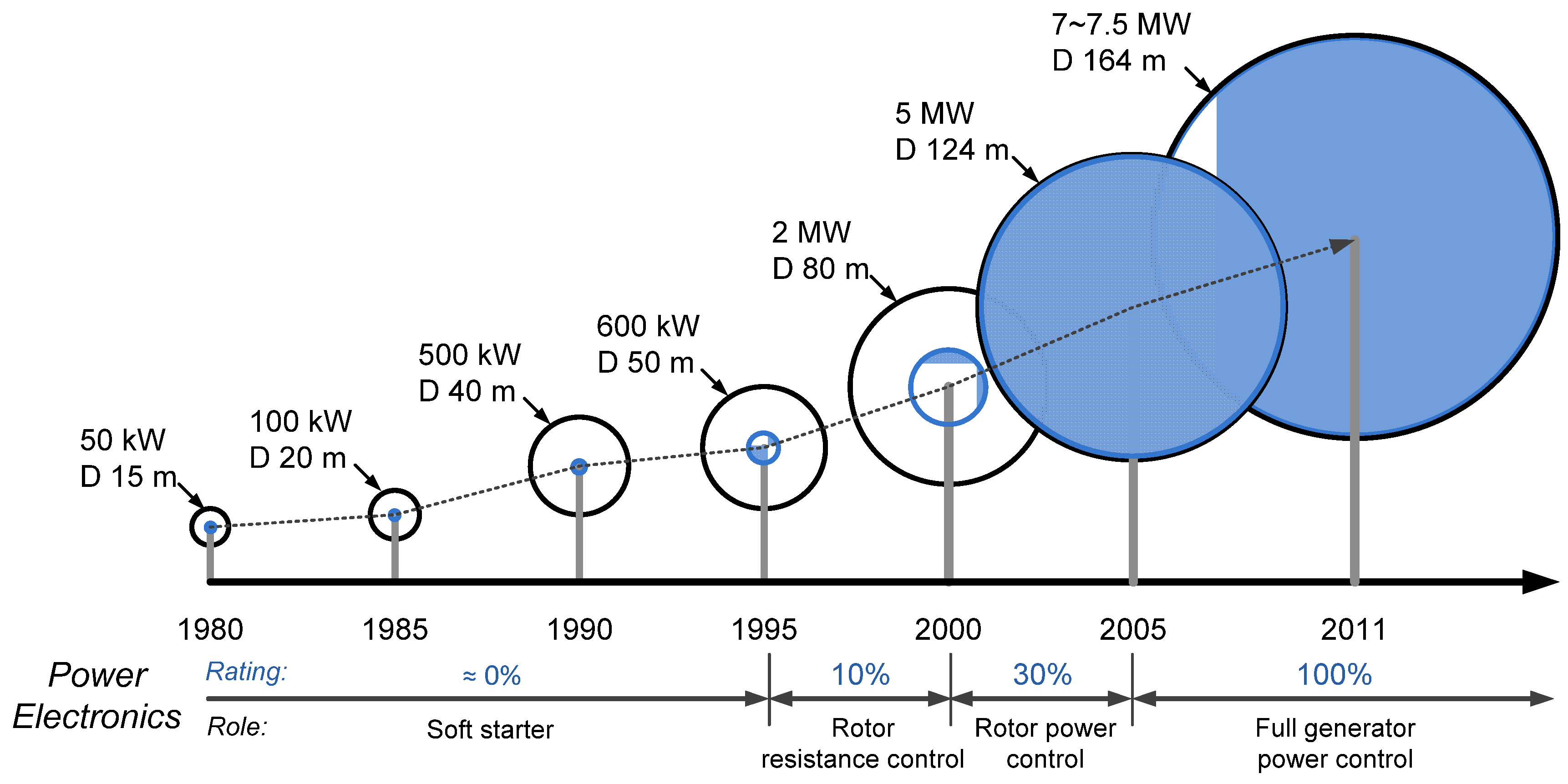
In order to meet the growing reliability and power controllability challenges, configurations for wind power generation have evolved from the no power electronic converter based system in the 1980s to the state-of-the-art full power electronic converter system, as indicated in
Figure 1. This is mainly because the full power converter system has full power controllability of the entire generated power from the wind turbines. Meanwhile, the simplified or eliminated gearbox and slip-ring can lead to more reliable mechanical structure of the system [
3].
Figure 1.
Evolution of wind turbines and power converters in the last 30 years (blue color indicates power level of converters in proportion to the wind turbines) [
5].
Figure 1.
Evolution of wind turbines and power converters in the last 30 years (blue color indicates power level of converters in proportion to the wind turbines) [
5].
Nevertheless, the larger capacity power electronic converters introduced with more stressed and expensive power semiconductors may trade off the lifetime and cost performance of the electrical parts in the full power converter based generation system. As a result, the reliability and cost related characteristics are critical when choosing power switching devices for the modern wind power converters.
The dominant power switching device choices as reported in the wind power industrial application are based on module packaging
Insulated Gate Bipolar Transistor (IGBT), press-pack packaging IGBT and the press-pack packaging
Integrated Gate Commutated Thyristor (IGCT). The three power semiconductor devices have quite different characteristics and are generally compared in
Table 1 [
5]. The module packaging technology for IGBT has a longer track record of applications and fewer mounting regulations. However because of the soldering and bond-wire connection of internal chips, module packaging devices may suffer from larger thermal resistance, lower power density and higher failure rates [
6]. The press-pack packaging technology improves the connection of chips by direct press-pack contacting, which leads to improved reliability (yet to be scientifically proven but known from industrial experience), higher power density (easier stacking for series connection) and better cooling capability with the disadvantage of higher cost compared to the module packaging devices. Press-pack IGCTs were introduced into the medium voltage converters in the 1990s and are already becoming state of the art in high power electric drives (e.g., for oil and gas application) but have not yet been significantly mass adopted in the wind turbine industry [
6,
7,
8].
Table 1.
Dominant power switching devices for modern wind power converters.
Table 1.
Dominant power switching devices for modern wind power converters.
| Characteristics | IGBT module | IGBT Press-pack | IGCT Press-pack |
|---|
| Power Density | Moderate | High | High |
| Reliability | Moderate | High | High |
| Cost | Moderate | High | High |
| Failure mode | Open circuit | Short circuit | Short circuit |
| Easy maintenance | + | - | - |
| Insulation of heat sink | + | - | - |
| Snubber requirement | - | - | + |
| Thermal resistance | Moderate | Small | Small |
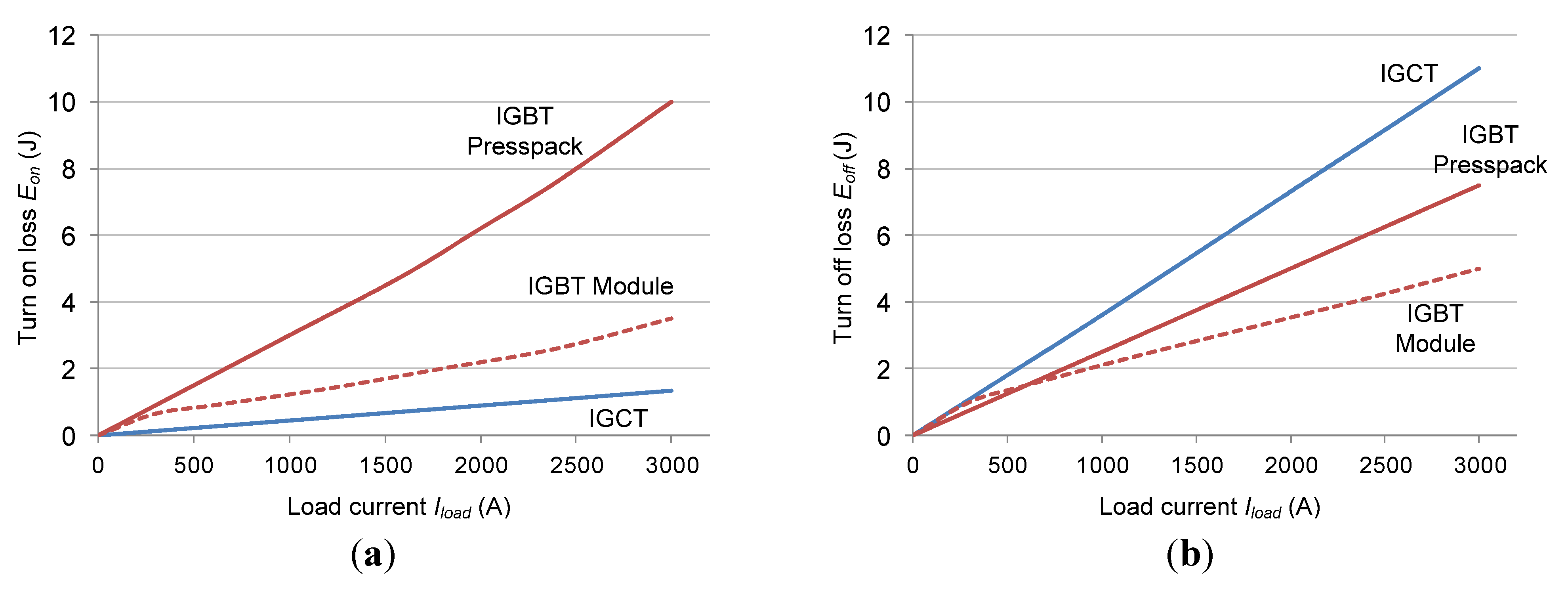
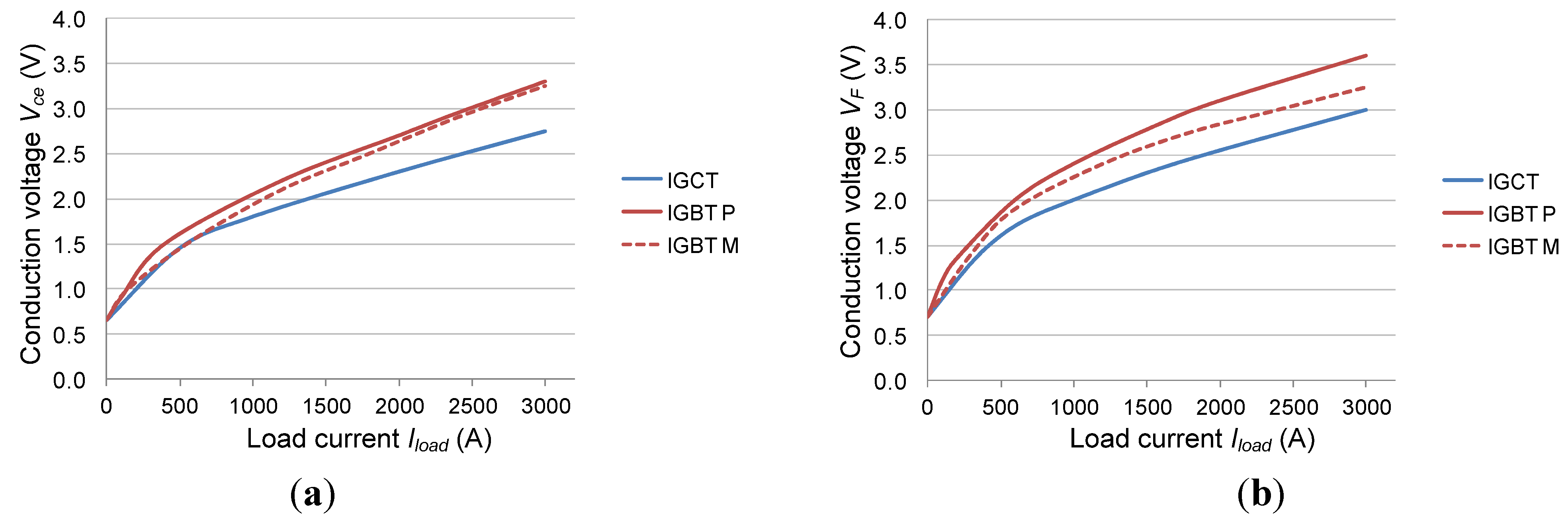
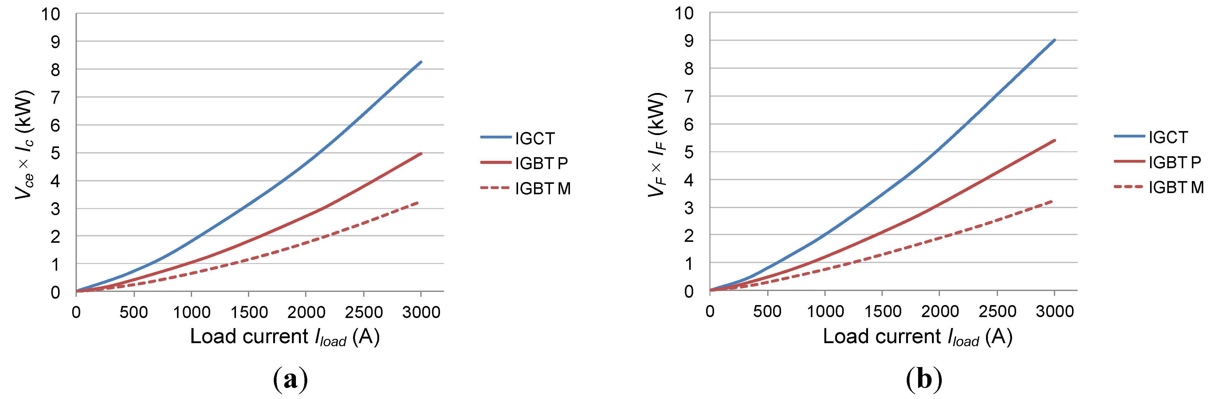
| Switching loss | Low | Low | High |
| Conduction loss | High | High | Low |
| Gate driver | Small | Small | Large |
| Major manufacturers | Infineon, Mitsubishi
ABB, Semikron, Fuji | Westcode, ABB | ABB |
| Medium voltage ratings | 3.3 kV / 4.5 kV / 6.5kV | 2.5 kV / 4.5 kV | 4.5 kV / 6.5 kV |
| Max. current ratings | 1.5 kV / 1.2 kA / 750 A | 2.2 kA / 2.4 kA | 2.1 kA / 1.3 kA |
According to [
6,
9,
10,
11,
12], the thermal cycling behavior inside the power switching devices is one of the key failure mechanisms and is closely related to its life time as well as the cost/size of the corresponding heat sink system. Therefore, it is interesting to investigate the thermal cycling related characteristics of the three important power switching devices applied in the wind power application. In this paper, the impact of the three important power switching devices on the thermal cycling of a 10 MW three-level Neutral-Point-Clamped wind power converter are evaluated under various operating conditions; the main focus will be on the grid connected inverter.
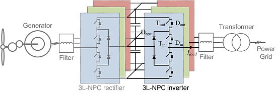
2. Wind Power Converter for Case Study
It is expected that 10 MW wind turbines with full-scale power converters will be the next long-term target to be conquered according to the current technology trends [
2,
3,
4,
5]. In most cases, the multi-level converter topologies will be expected to handle such high power with medium voltage ratings [
13]. As the most commercialized multilevel converter [
14,
15], three-level neutral-point-clamped (3L-NPC) topology seems to be a promising candidate [
16,
17], as shown in
Figure 2, where T
out represents the outer switch, D
out is the outer freewheeling diode, T
in is the inner switch, D
in is the inner freewheeling diode, and D
npc is the clamping diode. This configuration is selected for the analysis in this paper.
Figure 2.
A back-to-back three level neutral-point-clamped wind power converter system.
Figure 2.
A back-to-back three level neutral-point-clamped wind power converter system.
A 10 MW medium-voltage 3L-NPC wind power inverter is first designed for a case study. As summarized in
Table 2 [
18], all of the power devices have the commutated voltage of 2.8 kV in order to utilize the dominant 4.5 kV high-power semiconductors available on the market, and the rated DC bus voltage can be determined at 5.6 kV. Normal Phase-Disposition Sinusoidal-Pulse-Width-Modulation method for the 3L-NPC converter is applied. The carrier frequency is typically designed to be 800 Hz in order to reach an acceptable switching loss and respect the switching frequency limitation for the high power semiconductor devices. The output filter inductance is designed to limit the maximum voltage drop on inductor as 0.2 p.u.; the filter capacitance is not taken into account in this paper. For simplicity of analysis and to keep the analysis focus on the power loss and thermal behavior of the power semiconductors, the power grid is considered as three ideal AC voltage sources and the DC bus capacitance is assumed high. The used generator and wind turbine models can be found from [
19,
20].
Table 2.
Rated parameters of 10 MW 3L-NPC wind power inverter for case study.
Table 2.
Rated parameters of 10 MW 3L-NPC wind power inverter for case study.
| Converter items | Parameters |
|---|
| Rated output active power Po | 10 MW |
| DC bus voltage Vdc | 5.6 kV DC |
| * Rated primary side voltage Vp | 3.3 kV rms |
| Rated line-to-line grid voltage Vg | 20 kV rms |
| Rated load current Iload | 1.75 kA rms |
| Carrier frequency fc | 800 Hz |
| Filter inductance Lf | 1.14 mH (0.3 p.u.) |
Three power switching device solutions using IGCT press-pack, IGBT press-pack and IGBT module for the given 10 MW 3L-NPC wind power converter are listed in
Table 3, where the device ratings, configurations, total device numbers and used device models are indicated, respectively [
21,
22]; the maximum allowable junction temperature for all of the given power devices is 125 °C. It is noted that in order to justify and facilitate the comparison, each device solution is designed to handle the same load current up to 3.6 kA, therefore two 1.8 kA IGBT press-packs and three 1.2 kA IGBT modules have to be paralleled due to the limits of maximum available current rating for the corresponding power switching devices. The load current in each of the parallel device is assumed to be equally distributed. It is worth mentioning that the paralleling of power switching devices may change the loading profile significantly and has a strong impact on the loss, thermal, cost and power density performances of the converter. In this paper only the least paralleling number is considered for each of the power device solutions.
Table 3.
Three power switching device solutions for 10 MW 3L-NPC converter.
Table 3.
Three power switching device solutions for 10 MW 3L-NPC converter.
| Solutions | Main Switch (each) | Clamping Diode (each) | Device Numbers |
|---|
| IGCT Presspack | 1 × IGCT (3.6 kA/4.5 kV)
1 × Diode (3.6 kA/4.5 kV) | 1 × (3.6 kA/4.5 kV) Diode | 30 |
| IGBT Presspack | 2 × IGBT (1.8 kA/4.5 kV)
Integrated Diode | 2 × (1.8 kA/4.5 kV) Diode | 36 |
| IGBT Module | 3 × IGBT (1.2 kA/4.5 kV)
Integrated Diode | 3 × (1.2 kA/4.5 kV) Diode | 54 |
As can be seen in
Table 3, in order to achieve 10 MW power conversion, the power semiconductors needed for the three device solutions are quite different: the IGBT module solution consumes up to 80% more device numbers than the other two press-pack solutions. This is mainly because of the maximum current rating limits for a single IGBT module. When taking into account the extra auxiliary parts like drives, fans, heat sink, wires,
etc., the IGBT module solution may result in much lower power density and higher component counts, which may not be preferable in the wind power application.
4. Thermal Analysis of Different Device Solutions
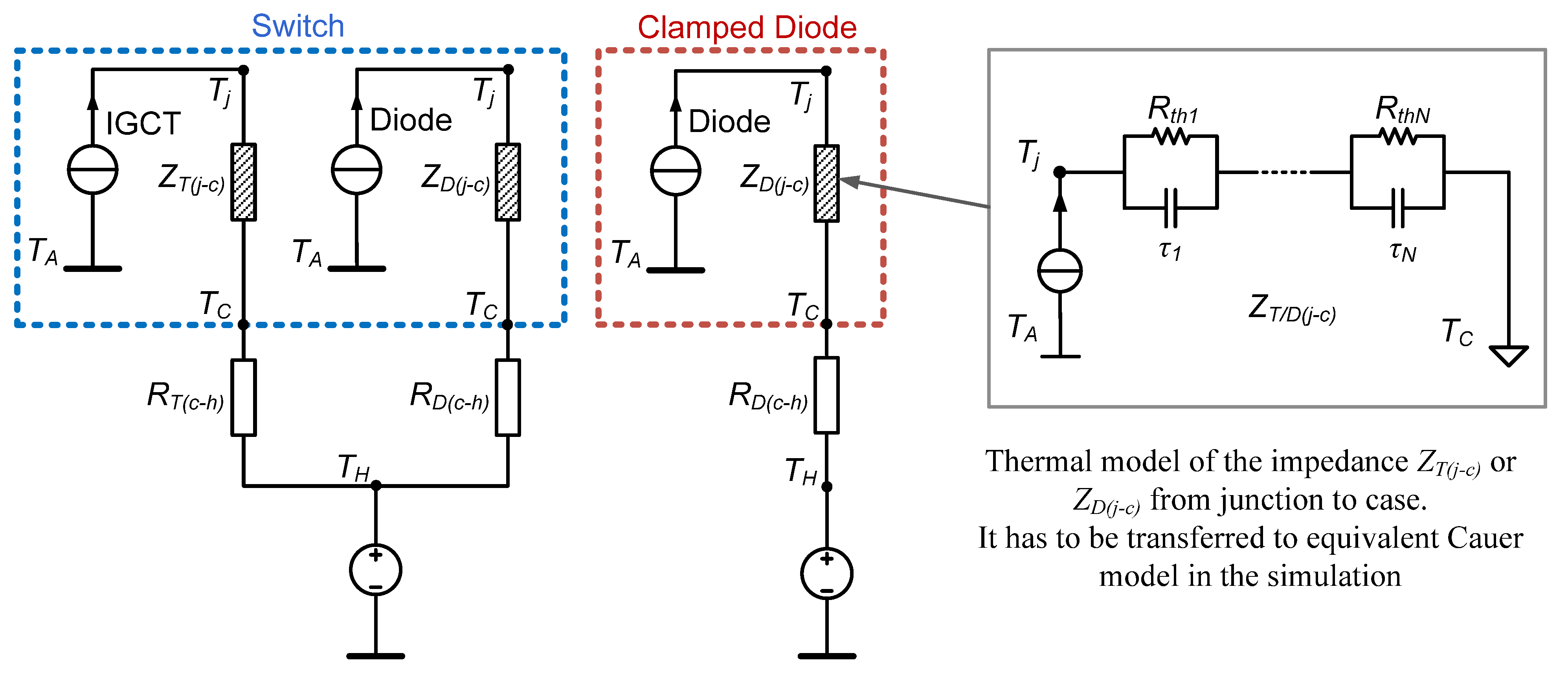
The thermal models for a single switch and clamping diode are indicated in
Figure 8 [
21,
22,
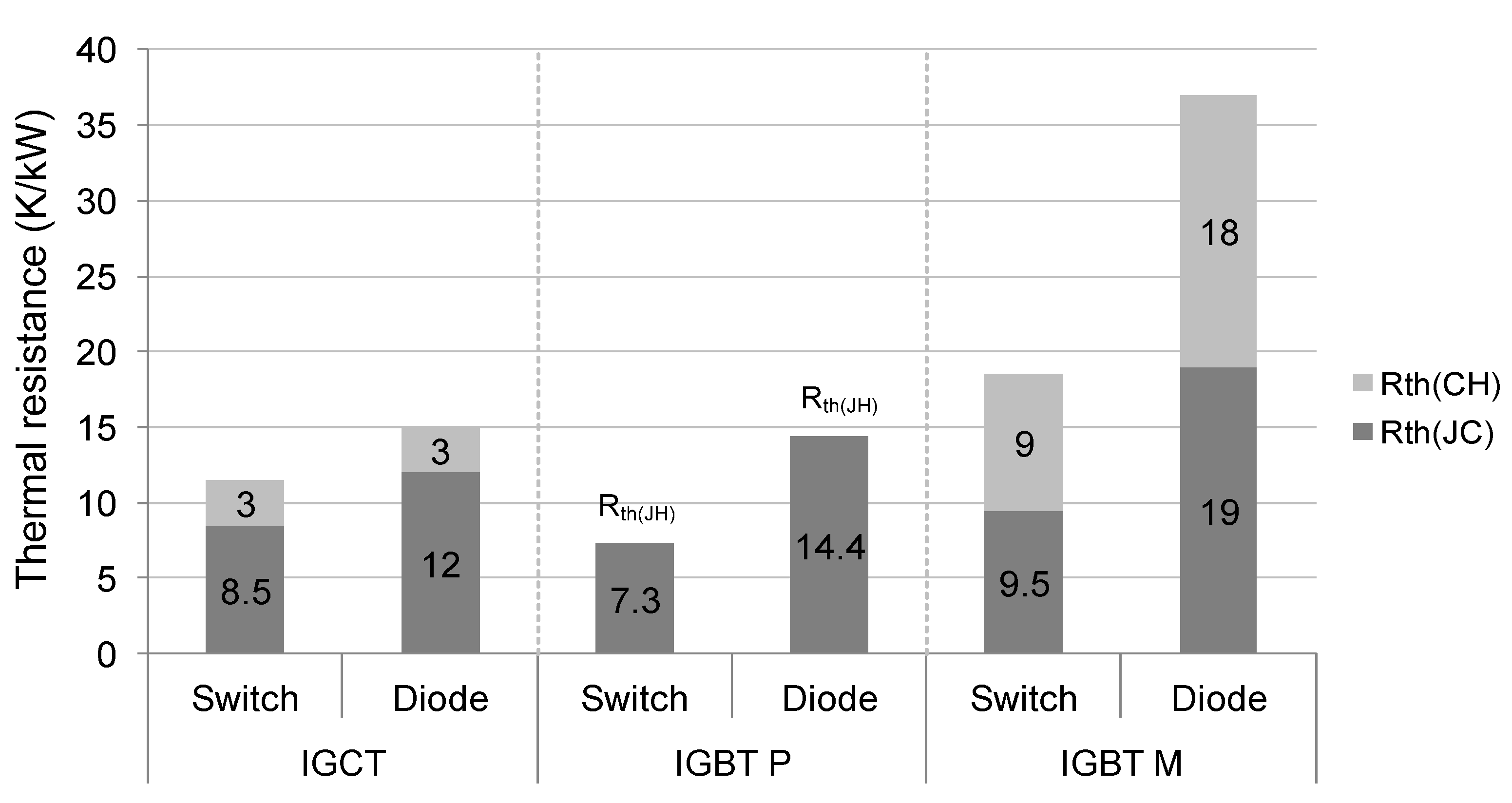
23] in which the thermal impedance from junction to case
Z(j–c) is modeled as a multi-layer Foster RC network. Each of the thermal parameters can be found from the manufacturer datasheets, where the thermal resistance
Rth will decide the steady state mean value of the junction temperature, and the thermal capacitance (with time constant τ) will decide the dynamic change or fluctuation of the junction temperature.
Figure 8.
Thermal model for the analysis and simulation of 3L-NPC converter.
Figure 8.
Thermal model for the analysis and simulation of 3L-NPC converter.
Note: Tj: junction temperature, TC: case temperature, TH: heat sink temperature, TA: ambient temperature; Z(j–c): thermal impedance from junction to case, Z(c–h): thermal impedance from case to heat sink.
It is noted that normally the IGBT manufacturer will only provide thermal parameters inside IGBT modules with Foster RC network. In order to establish the complete thermal models from junction to the ambient, the thermal impedance of
ZT/D(j-c) has to be transferred to the equivalent Cauer RC network to facilitate the thermal impedance extension outside IGBT modules [
27]. Because the temperature of the heat sink
TH is normally much lower and more stable compared to the junction temperature
Tj in a properly designed converter system, the heat sink temperature is considered as a constant value at 60 °C in this paper. However, the heat sink temperature may strongly depend on the operation site and the design of the heat sink system.
After the parameters for the converter as well as the loss and thermal models for the power switching devices are settled, some important operation modes of the 3L-NPC converter can be simulated. The simulations are carried out based on PLECS blockset in Simulink [
27], and the simulation parameters are consistent with the ones in
Table 2 and
Table 3; the main focus will be on the grid connected inverter.
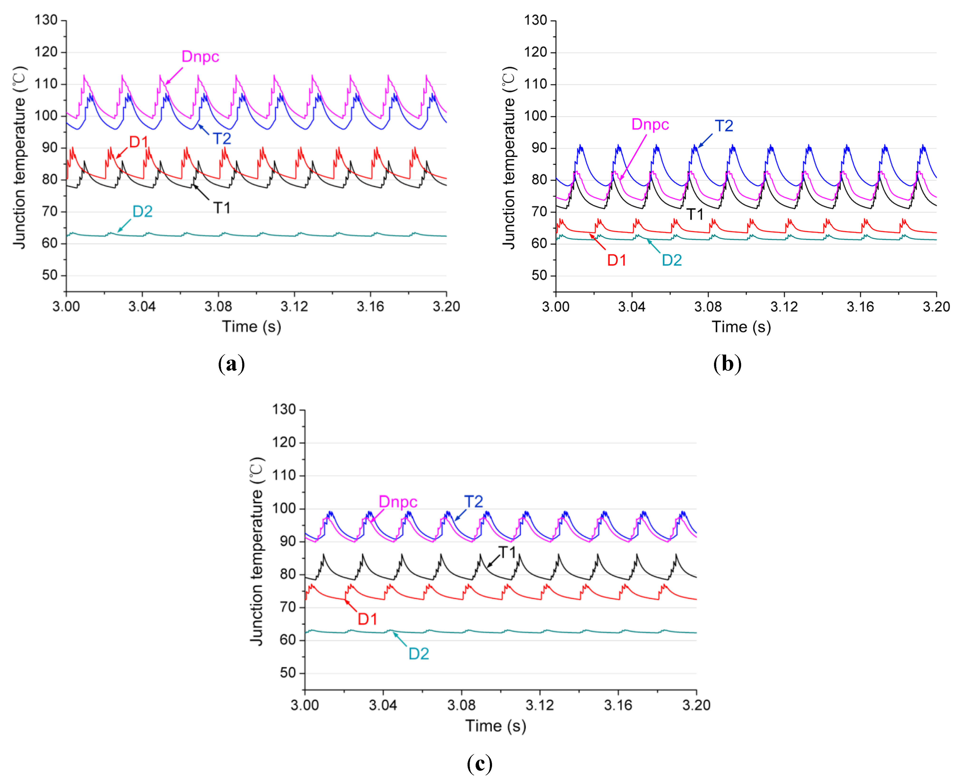
4.1. Normal operation
The thermal cycling performance of the 3L-NPC wind power inverter when the wind turbine is running at rated wind speed 12 m/s and rated grid voltage will first be analyzed.
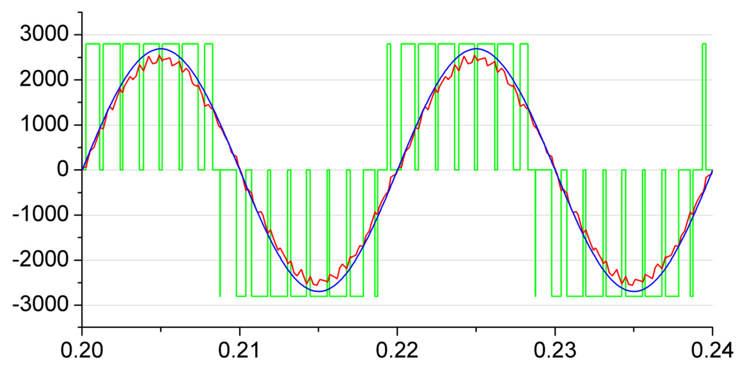
Figure 9 shows the converter output voltage pulses, phase current and grid voltage under rated and normal conditions of the wind turbines. It can be seen that the load current is in phase with the grid voltage,
i.e., power factor
PF = 1.
Figure 9.
Simulation outputs of 3L-NPC inverter under rated normal operation (output voltage pulses-green, grid voltage-blue, phase current-red, Vg = 1 p.u., PF = 1, vw = 12 m/s, DC bus voltage VDC = 1 p.u.).
Figure 9.
Simulation outputs of 3L-NPC inverter under rated normal operation (output voltage pulses-green, grid voltage-blue, phase current-red, Vg = 1 p.u., PF = 1, vw = 12 m/s, DC bus voltage VDC = 1 p.u.).
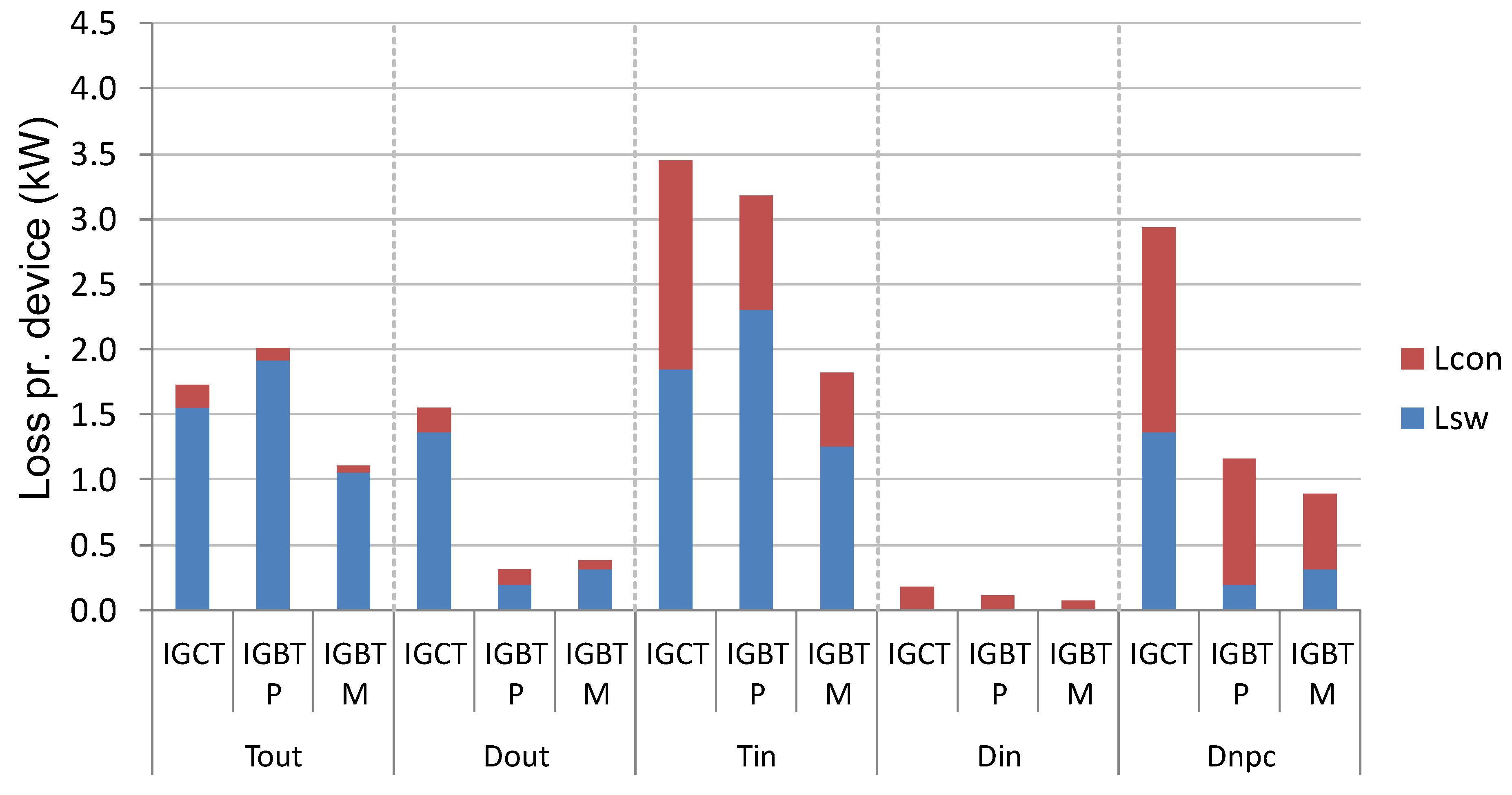
4.1.1. Loss Distribution
The loss calculation method is based on the same idea as in [
26,
28], which is a commonly accepted method for the loss evaluation of power semiconductor devices. It is noted that the switching loss profile of the chosen switching devices only has the test condition at 125 °C on the datasheet; the loss models in this paper are therefore considered temperature independent during the simulation. However, if the device characteristics under other temperatures are provided, the loss model with junction temperature dependence can be established and simulated by iteration in the simulation software.
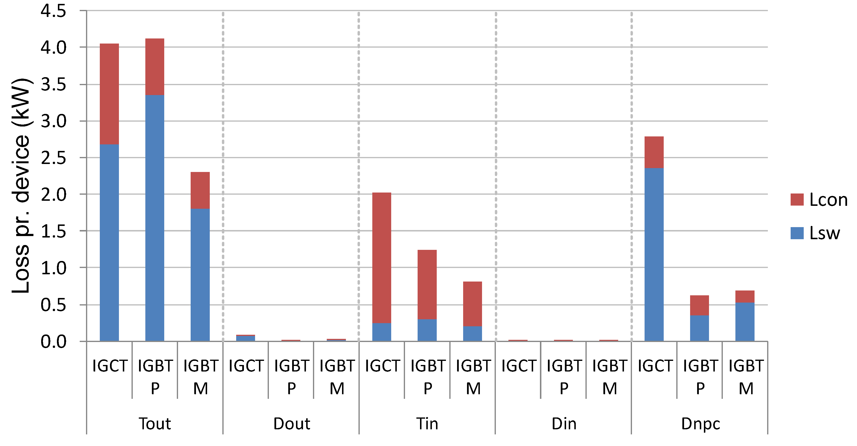
The loss distribution of the 3L-NPC converter with different device solutions under the normal rated condition is shown in
Figure 10, where only one single device is indicated if parallel power device solutions are applied.
Figure 10.
Loss distribution for different power switching devices under normal operation of
Figure 9 (
Lcon means conduction loss-red,
Lsw means switching loss-blue).
Figure 10.
Loss distribution for different power switching devices under normal operation of
Figure 9 (
Lcon means conduction loss-red,
Lsw means switching loss-blue).
As it can be seen from
Figure 10, the major losses for all the device solutions are consumed by the outer switches T
out, inner switches T
in and the clamping diodes D
npc under normal operation of the wind power converter. The IGCT solution shows significantly larger loss in D
npc due to larger switching loss; on the other hand the IGBT module solution shows significantly lower overall loss level especially in T
out.
4.2. Low-Voltage-Ride-Through Operation
The simulation output of the 3L-NPC inverter undergoing low voltage rid through (LVRT) operation is shown in
Figure 13, in which the grid voltage is set to 0.05 p.u. of the rated value as a severe voltage dip, and the converter has to provide 100% rated reactive current according to the grid codes [
29,
30]. It can be seen that the phase current lags 90 degrees to the grid phase voltage, and the inverter achieves 100% rated reactive current injection (1.75 kA rms) into the power grid.
Figure 13.
Simulation outputs of 3L-NPC inverter under LVRT operation (output voltage pulses-green, grid voltage-blue, phase current-red, Vg = 0.05 p.u., 100% rated reactive current, DC bus voltage VDC = 1.1 p.u.).
Figure 13.
Simulation outputs of 3L-NPC inverter under LVRT operation (output voltage pulses-green, grid voltage-blue, phase current-red, Vg = 0.05 p.u., 100% rated reactive current, DC bus voltage VDC = 1.1 p.u.).
4.2.1. Loss Distribution
The loss distribution of the 3L-NPC inverter undergoing the given LVRT operation is shown in
Figure 14, where different device solutions are indicated and compared. It can be seen that the loss distribution is quite different from the one undergoing normal operation in
Figure 10; T
in has the highest power loss for all of the device solutions. The IGCT solution again shows significantly larger loss in D
npc, while the IGBT module solution has the lowest power loss level.
Figure 14.
Loss distribution for different power switching device solutions under LVRT operation of
Figure 13 (Lcon means conduction loss-red, Lsw means switching loss-blue).
Figure 14.
Loss distribution for different power switching device solutions under LVRT operation of
Figure 13 (Lcon means conduction loss-red, Lsw means switching loss-blue).
4.3. Wind Gust Operation
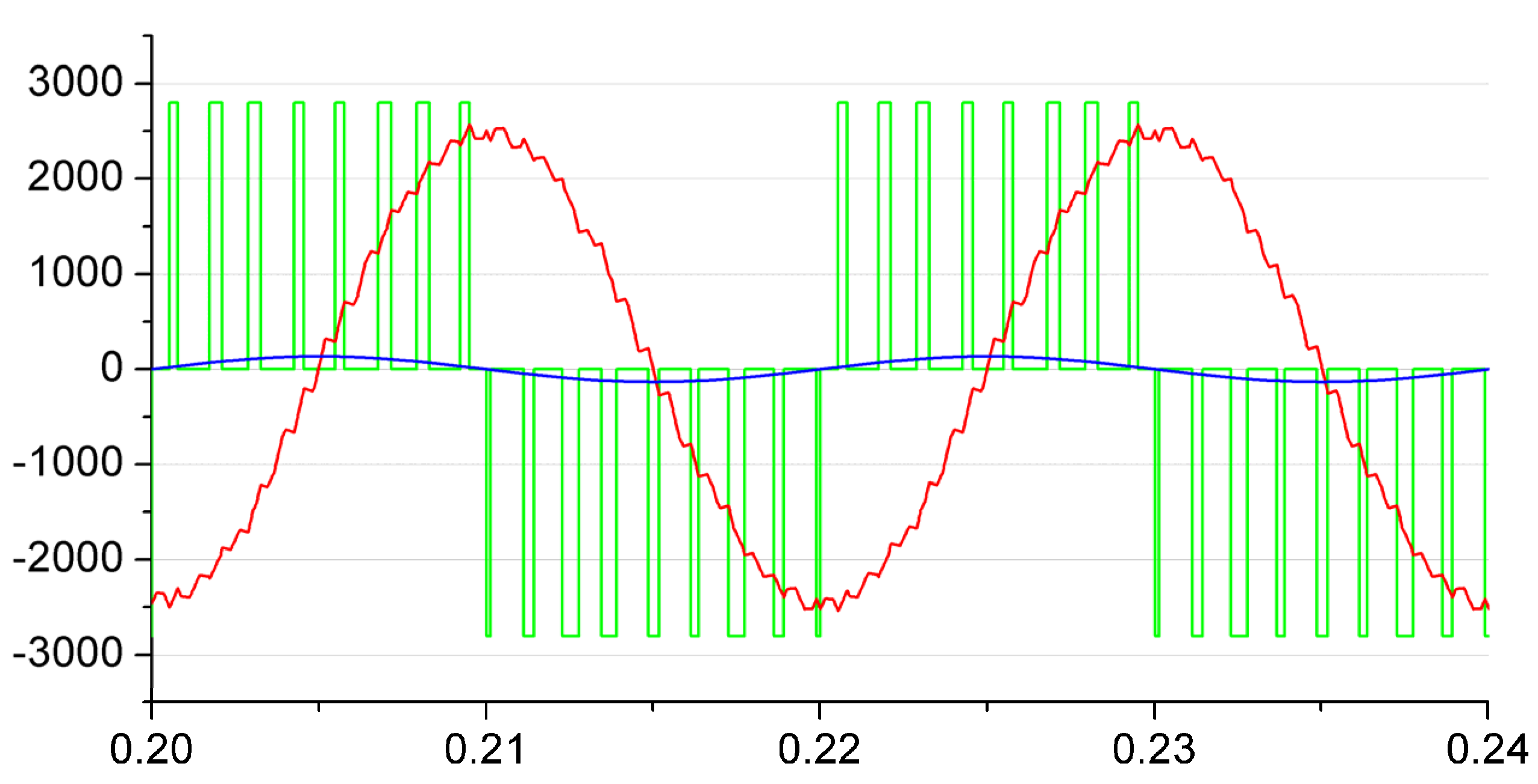
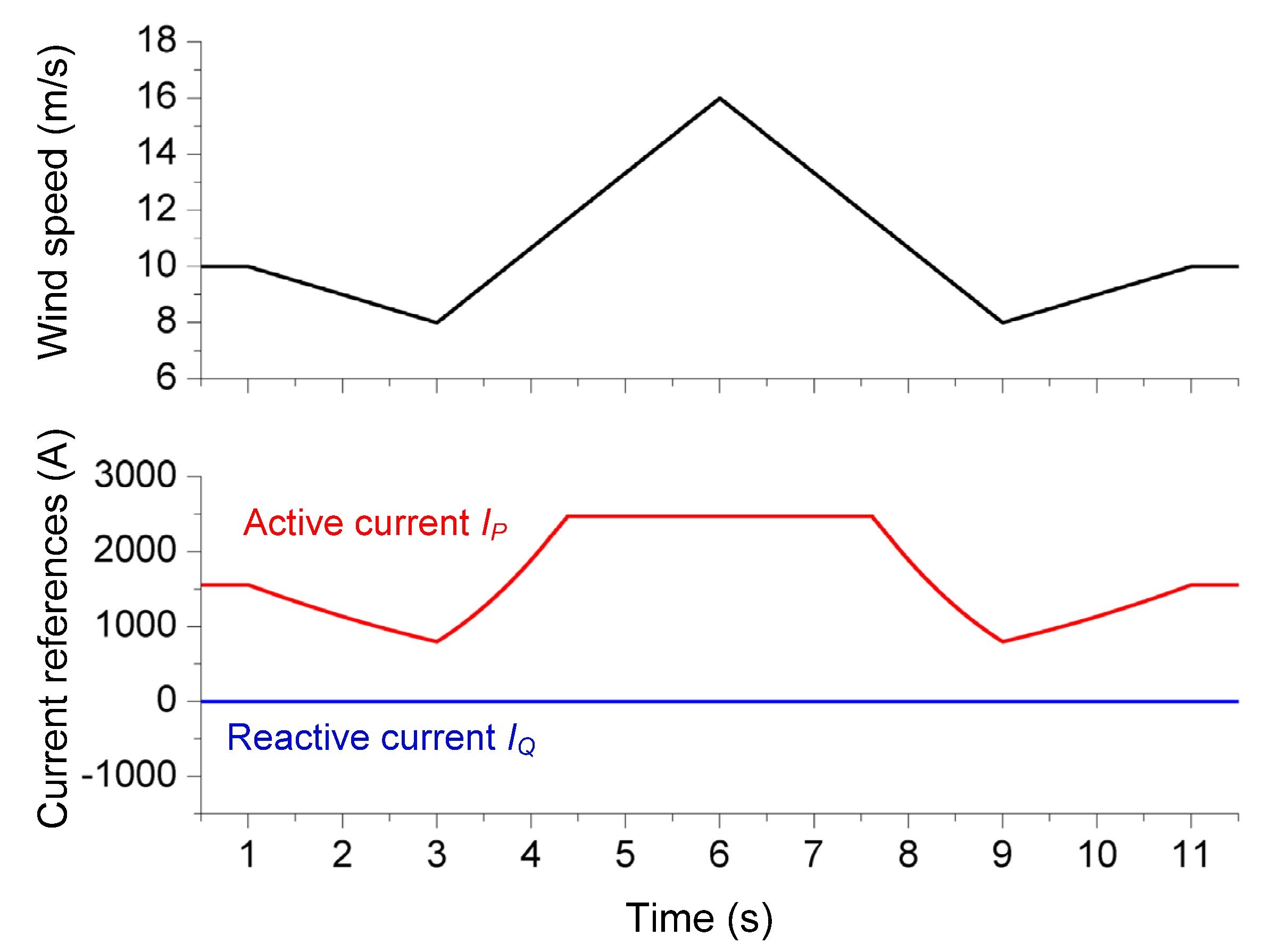
The wind gust operation of wind turbines may impose power switching devices with large thermal cycling amplitude and longer time disturbances compared to the LVRT and normal operation modes. According to the one-year return period wind gust definition by IEC standards [
31], a wind gust condition for a case study is indicated in
Figure 17, where the wind speed is set from 10 m/s dropping to 8 m/s and rising to 16 m/s; the reverse fashion is then continued. The active current reference of the converter is accordingly changed with the wind speed referring to the wind turbine model in [
20].
Figure 17.
Wind speed and current references of grid side 3L-NPC inverter in a defined wind gust.
Figure 17.
Wind speed and current references of grid side 3L-NPC inverter in a defined wind gust.
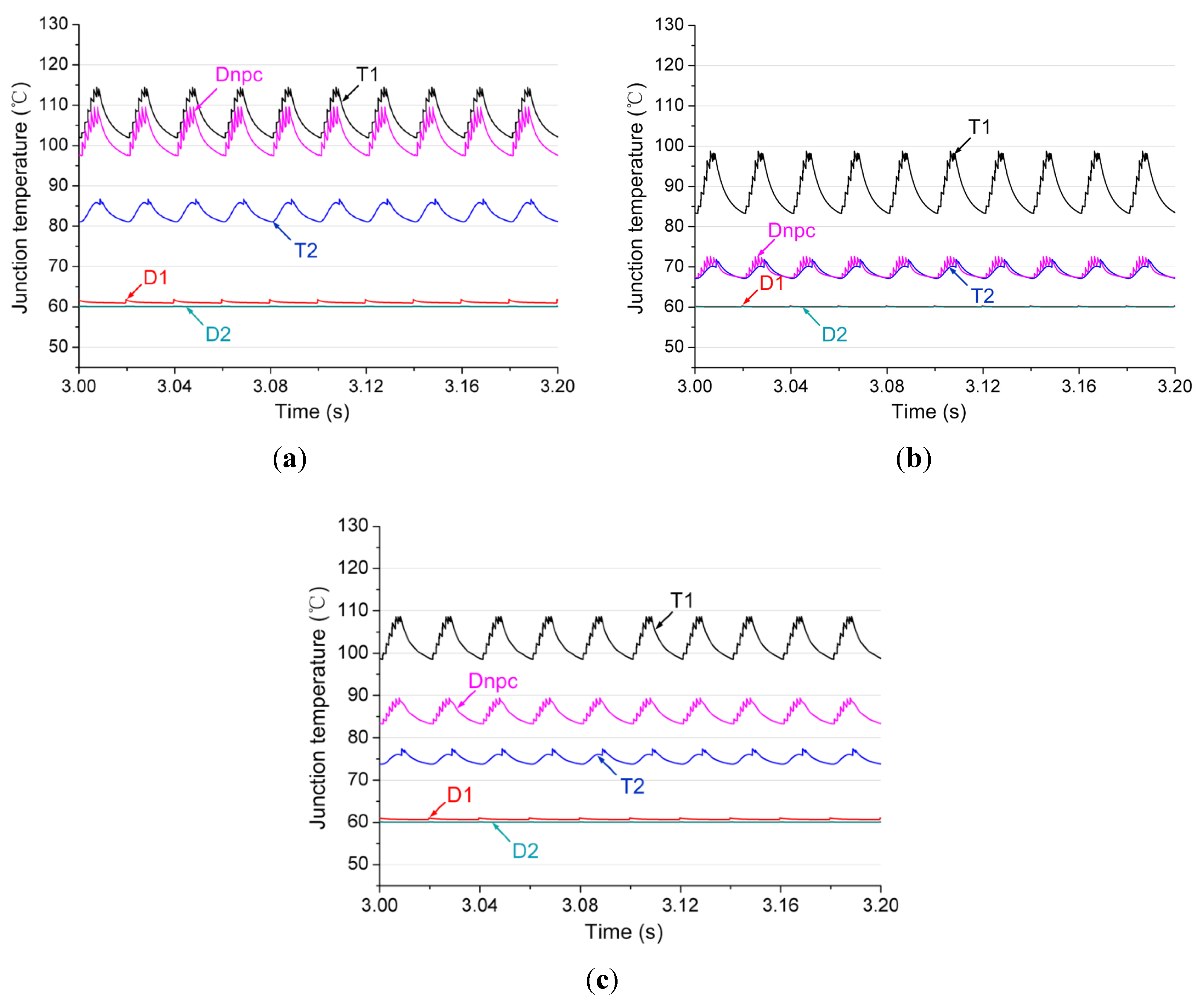
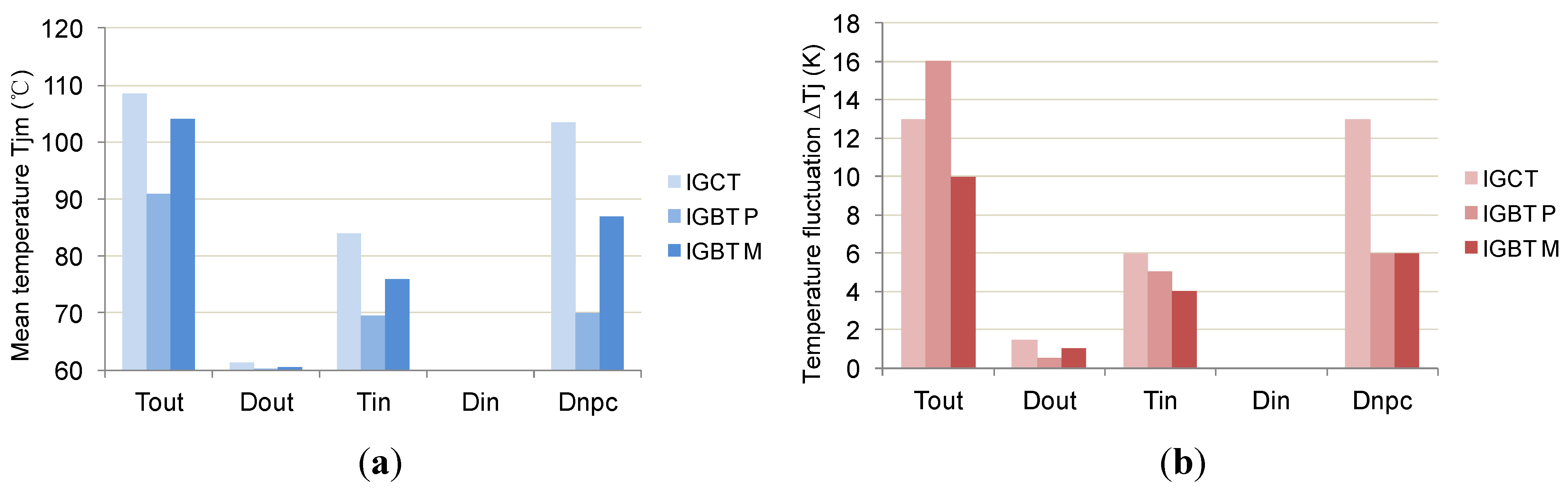
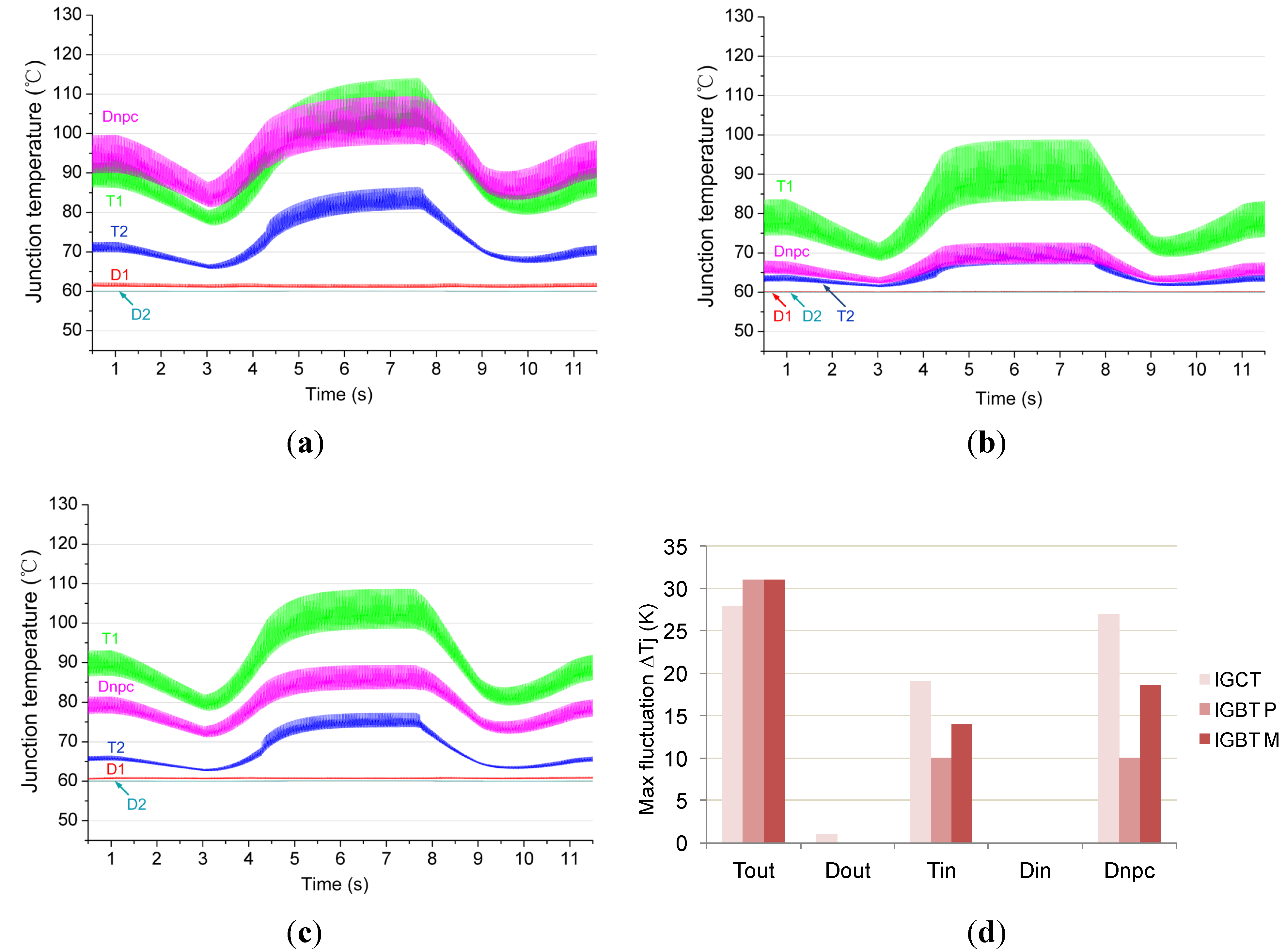
The junction temperature distributions of the target 3L-NPC inverter during the given wind gust operation condition are indicated in
Figure 18. It is obvious that three device solutions show significant differences in the most stressed devices, temperature fluctuation amplitude, and thermal distribution.
The maximum junction temperature fluctuation amplitudes with different device solutions are summarized in
Figure 18(d). It can be seen that the temperature in T
out is the most fluctuated device in all of the proposed solutions, and the IGCT solution shows more temperature fluctuation amplitude in T
in and D
npc under the given wind gust defined by the IEC standards.
5. Conclusions
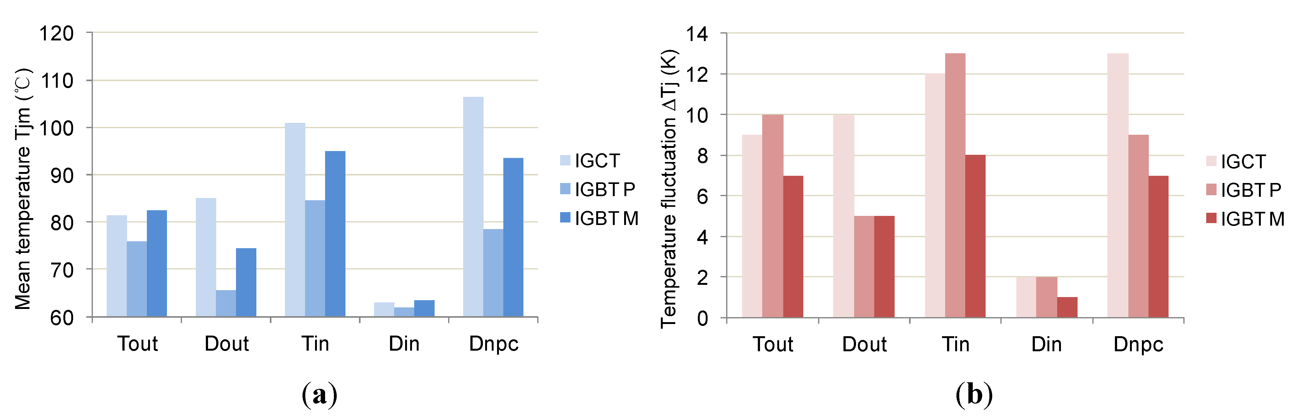
The thermal performance of power switching devices is important for modern wind power converter systems. It is found that the thermal related characteristics of the three dominant power switching devices in wind power application are quite different.
For all of the power switching device solutions in the 3L-NPC grid side inverter, the outer switches Tout, clamping diodes Dnpc and inner switch Tin are likely to become the most stressed devices under various important operation modes of the wind turbines and therefore they are critical components for the 3L-NPC wind power converter. The performance of the outer freewheeling diode Dout and inner freewheeling diode Din are less important because they are barely used.
Regarding the most stressed devices Tout, Tin and Dnpc, the three device solutions show quite different loading behaviors because of different power loss and thermal impedance characteristics: for the IGCT solution, the switching loss in the diode is much larger because of the normally used clamping circuit. This disadvantage may lead to much higher junction temperature in Dnpc in comparison with the other two IGBT solutions. The IGBT press-pack solution tends to have larger switching loss in the switch. However because of smaller thermal resistance, it shows a junction temperature level in the switches similar to the IGCT solution, but with much better thermal performance in the clamping diode. The IGBT module solution shows the best loss performances among the three device solutions, but due to much larger thermal resistance especially from case to heat sink, the junction temperature level is generally high. It is noted that the IGBT module solution may result in large component counts in a 10 MW power conversion system, which may not be preferable in the wind power application.
Finally, it is worth mentioning that the paralleling of power switching devices may change the loading profile significantly and has a strong impact on the loss, thermal, cost and power density performances of the converter; the parallel numbers of power switching devices should thus be carefully evaluated in the design process.


