Topology of a Bidirectional Converter for Energy Interaction between Electric Vehicles and the Grid

Abstract
:1. Introduction

| Region | Charging Method | Nominal Supply Voltage | Maximum Current |
|---|---|---|---|
| North America | AC Level 1 | Single phase 120 V AC | 12 A |
| Single phase 120 V AC | 16 A | ||
| AC Level 2 | Single phase 240 V AC | ≤80 A | |
| DC Level 1 | 200–500 V DC | ≤80 A | |
| DC Level 2 | 200–500 V DC | ≤200 A | |
| China | 1 | Single phase 220 V AC | 16 A |
| 2 | |||
| 3 | 32 A | ||
| 4 | 400 V/750 V DC | 125 A | |
| 250 A |
- (1)
- It eliminates the bulky and expensive DC intermediate link capacitors and the inductor in the bidirectional DC-DC stage of two-stage topologies, resulting in reduced component counts, smaller size, lighter weight, and higher power density.
- (2)
- By removing the expensive DC link capacitors and special customized DC-DC inductor in the typical two-stage topologies, the cost of passive components is reduced significantly. Furthermore, in contrast to two-stage topologies, four AC-side switches in our converter work under low frequency and low voltage stress, leading to less expensive component selection and lower cost on active components.
- (3)
- For the same inductance and switching frequency, this topology has less harmonic components than unipolar/bipolar modulated single-phase PWM converters that act as the first stage of the two-stage converters.
- (4)
- With the same ripple factor and switching frequency, inductance L of this topology is much smaller, leading to improved dynamic response after applying suitable feedback control systems.
- (5)
- Due to lower losses on passive components, lower conduction losses on low voltage stress switches, and four zero-switching-loss active switches, this topology is of much higher energy efficiency (soft-switching of the bidirectional DC-DC stage in the two-stage topologies cannot be guaranteed, especially when loads vary in a wide range or power flow varies).
- (6)
- Elimination of electrolytic capacitors in the DC intermediate link, and one-stage control system (which can be implemented by one micro control unit, in contrast to the typical topologies in which two controllers are needed) enhance converter reliability and reduce complexity.
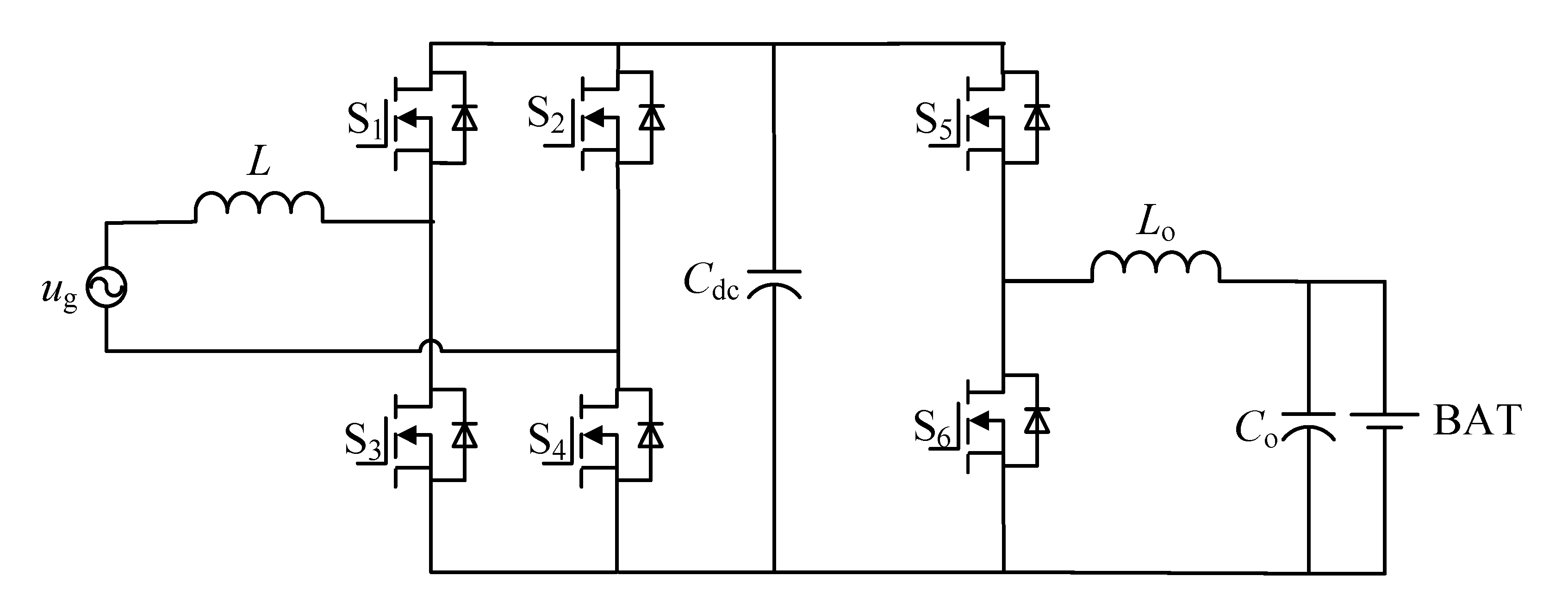
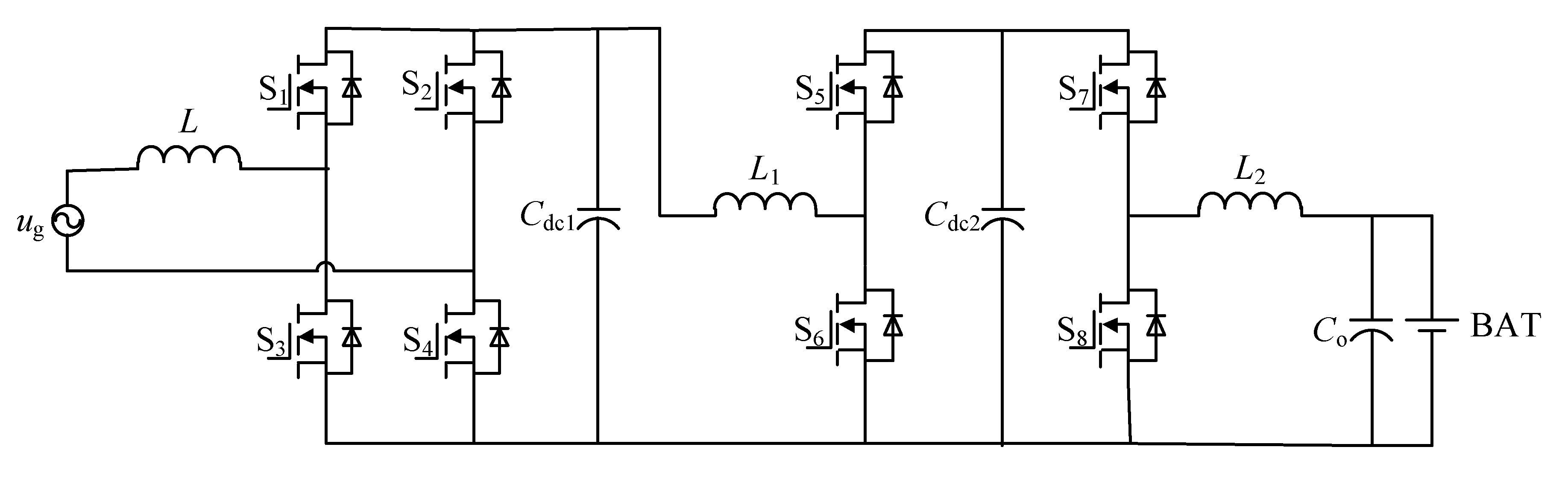
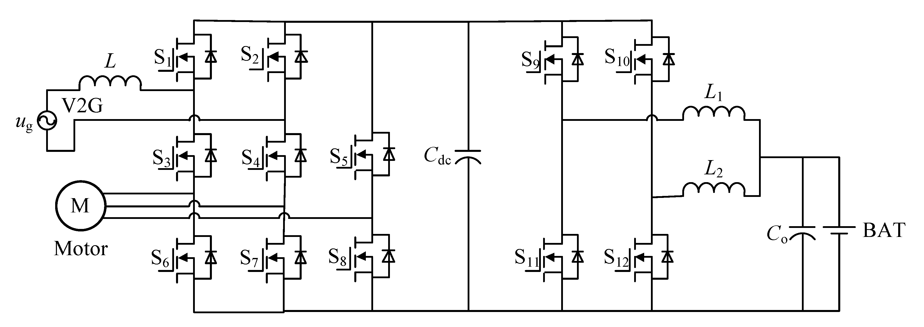
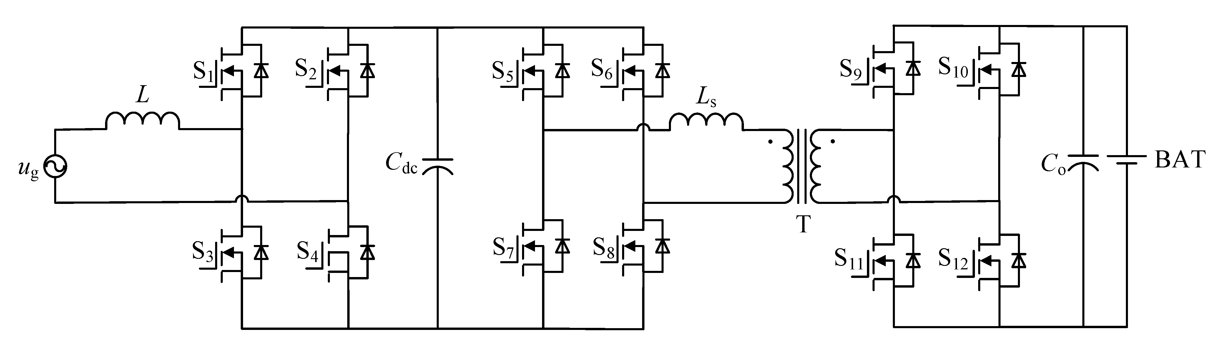
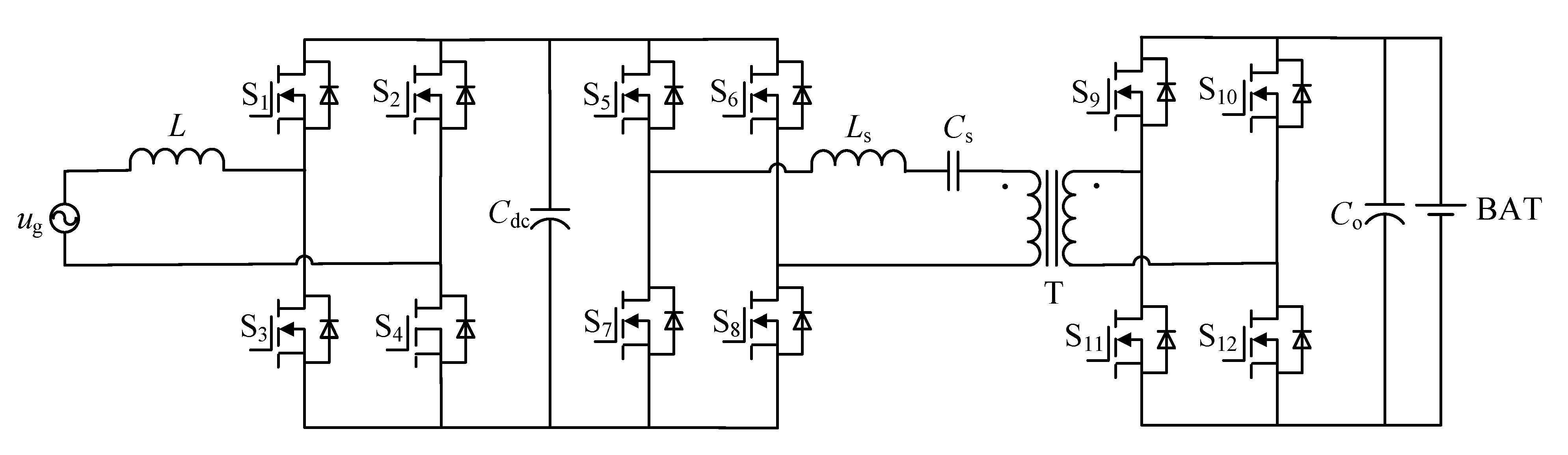
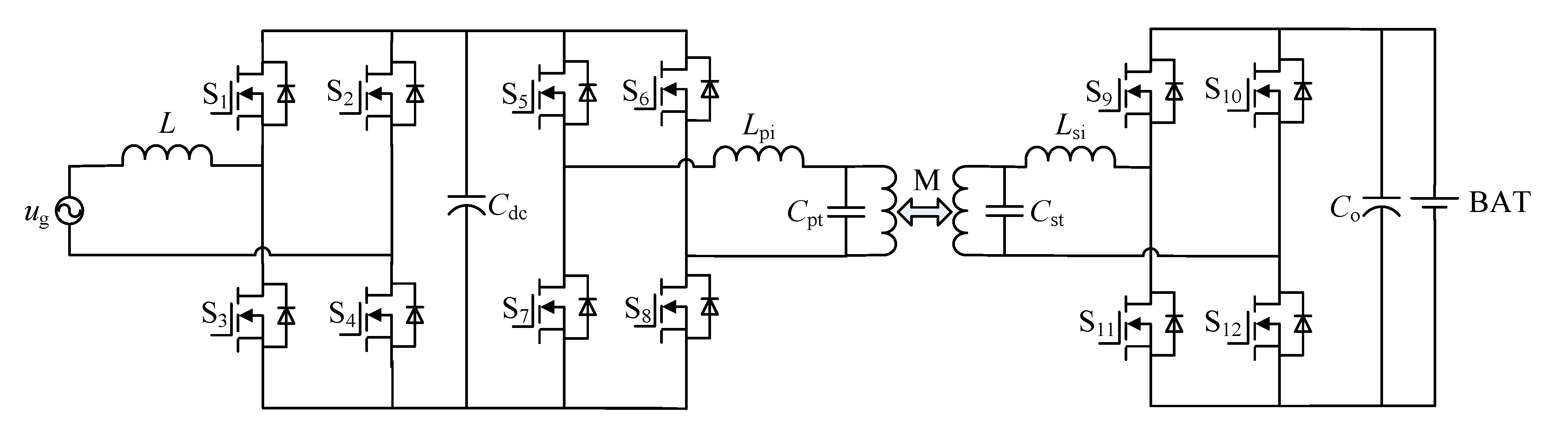
2. Typical Topologies of Bidirectional Converters for Connecting Electric Vehicles and Grid


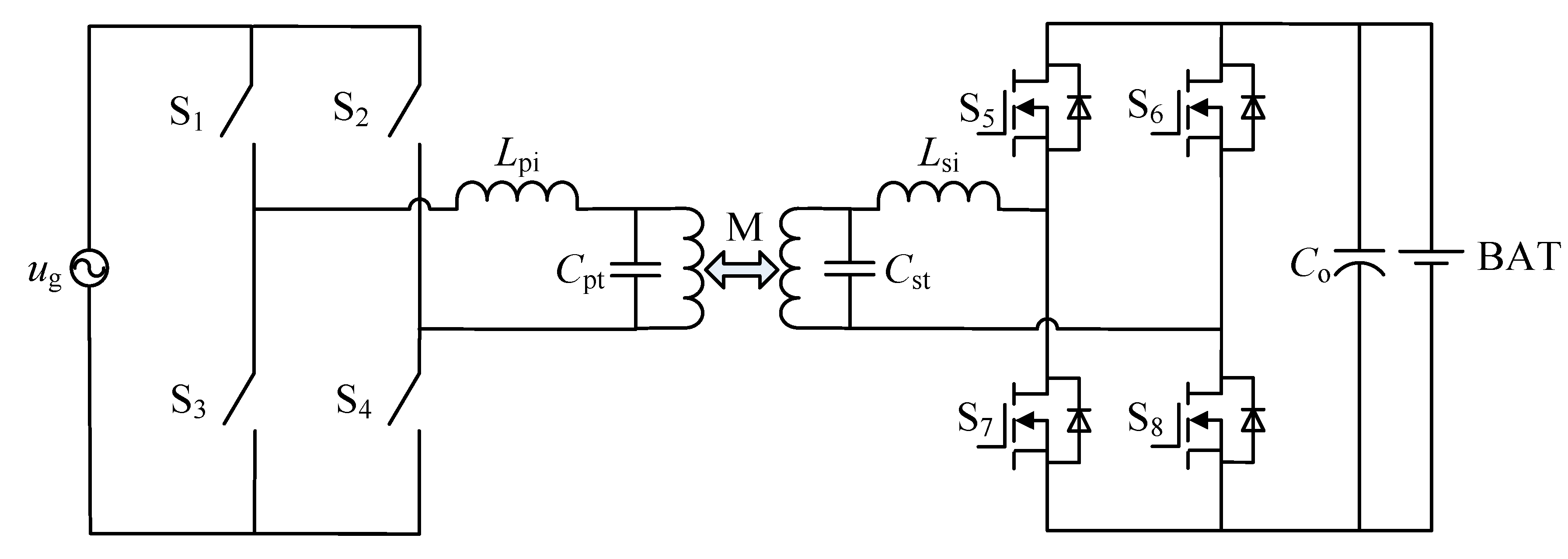
3. Novel High Power Factor Bidirectional Single-Stage Full-Bridge Topology
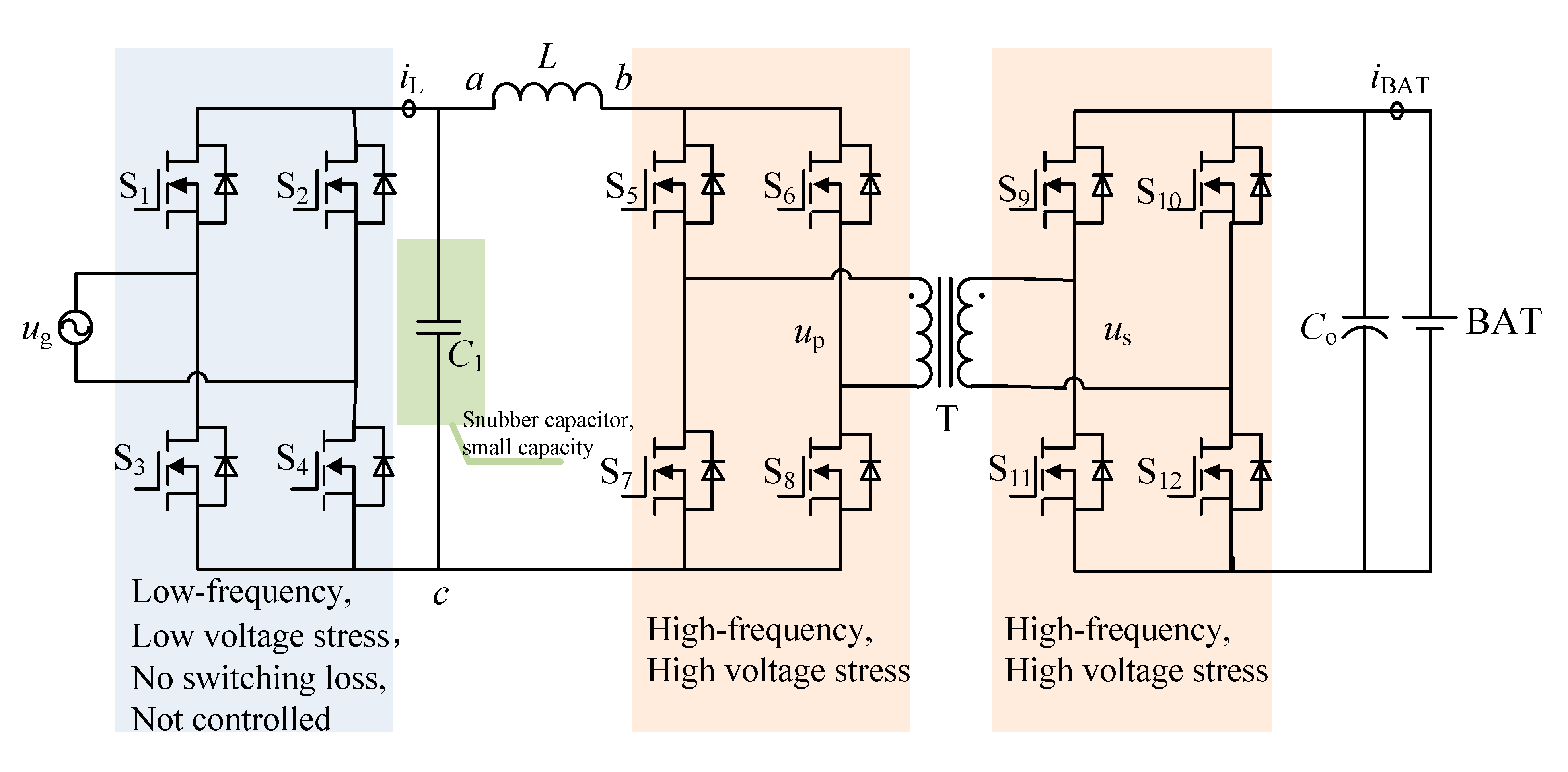
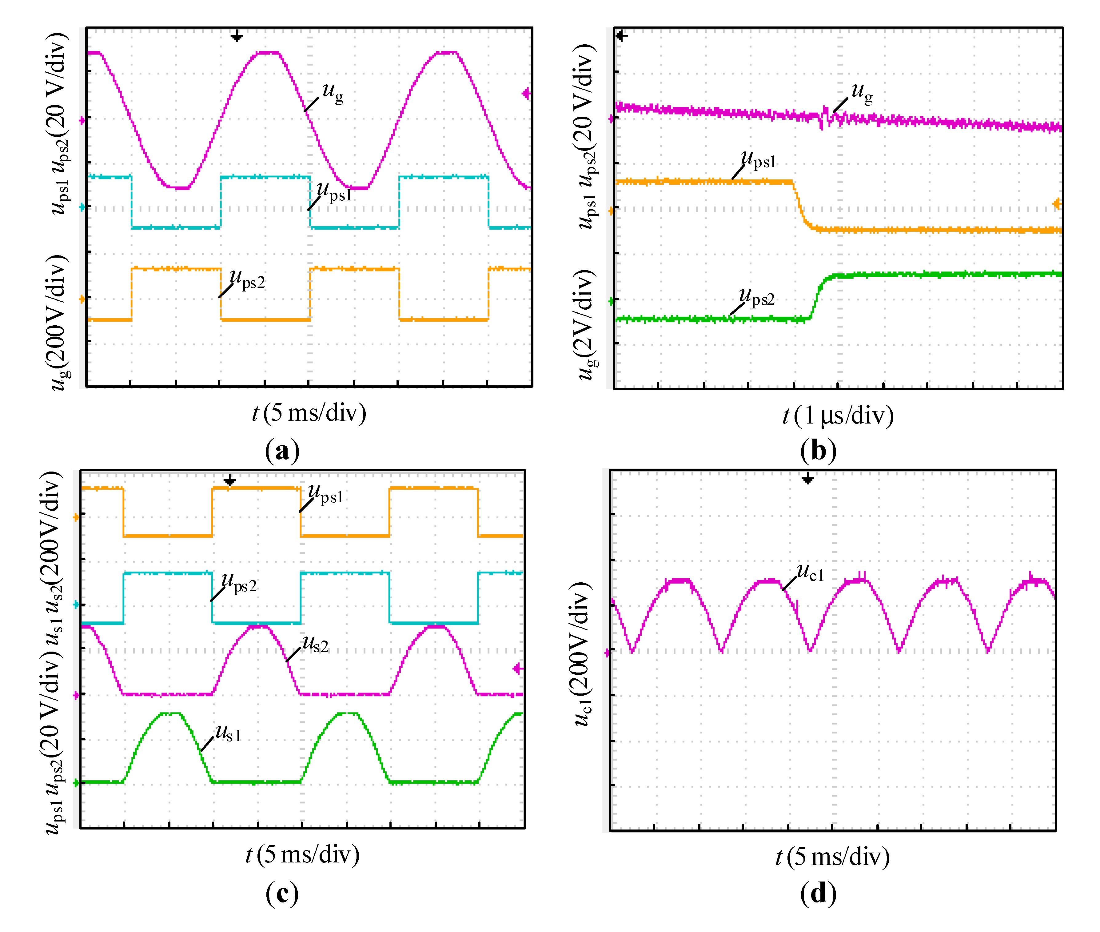
3.1. Topology of the Novel Converter

3.2. Operational Principles

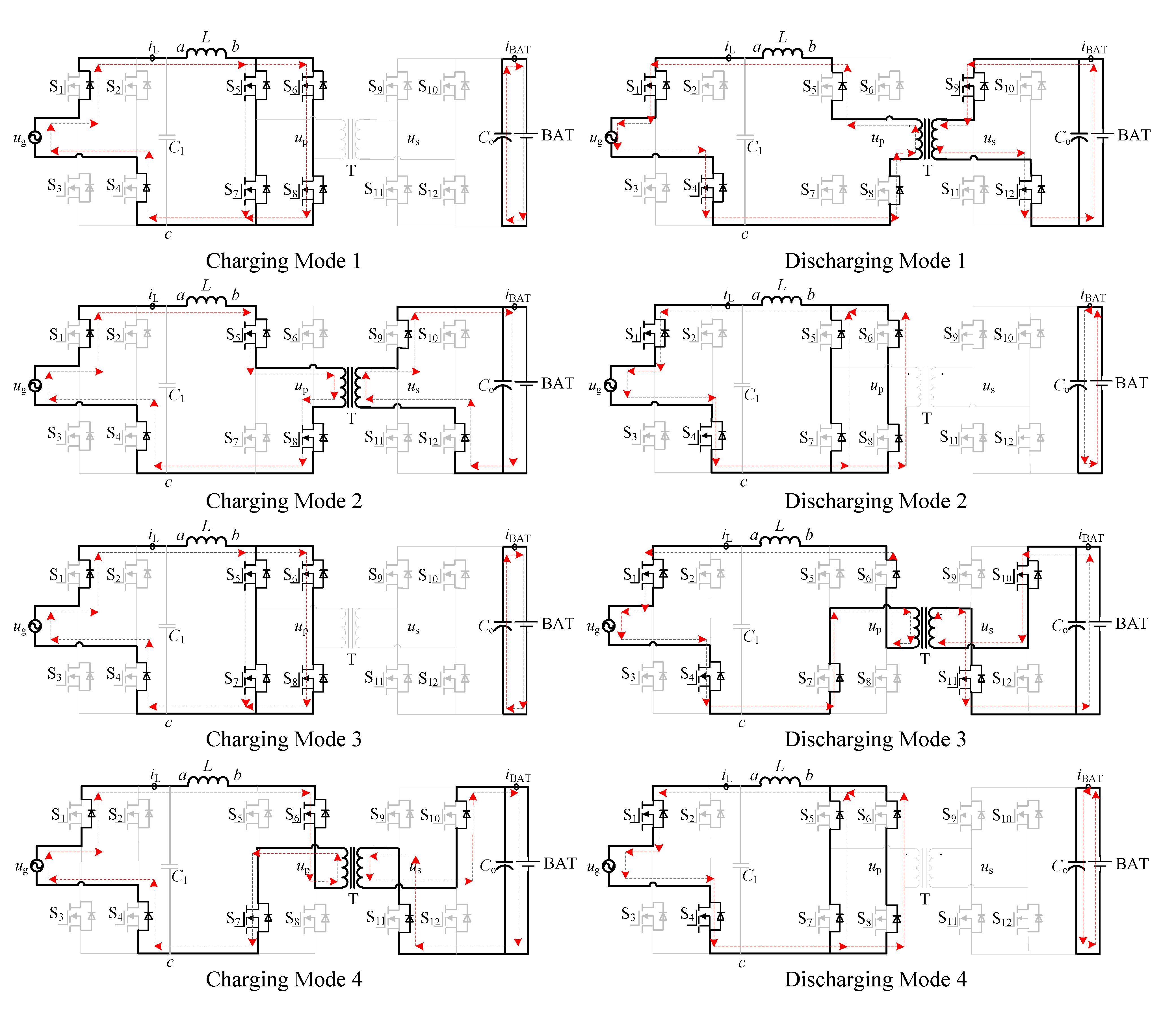
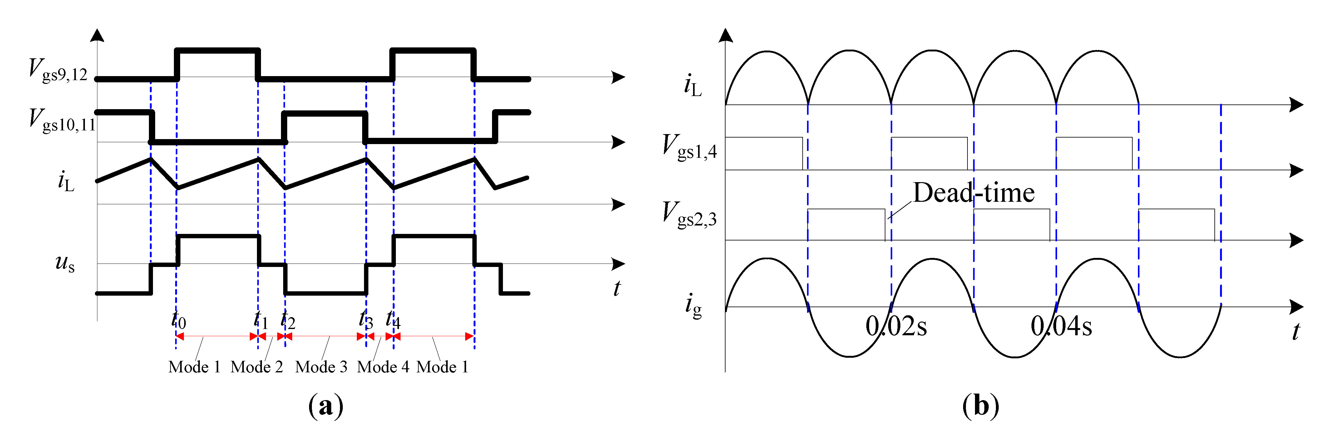
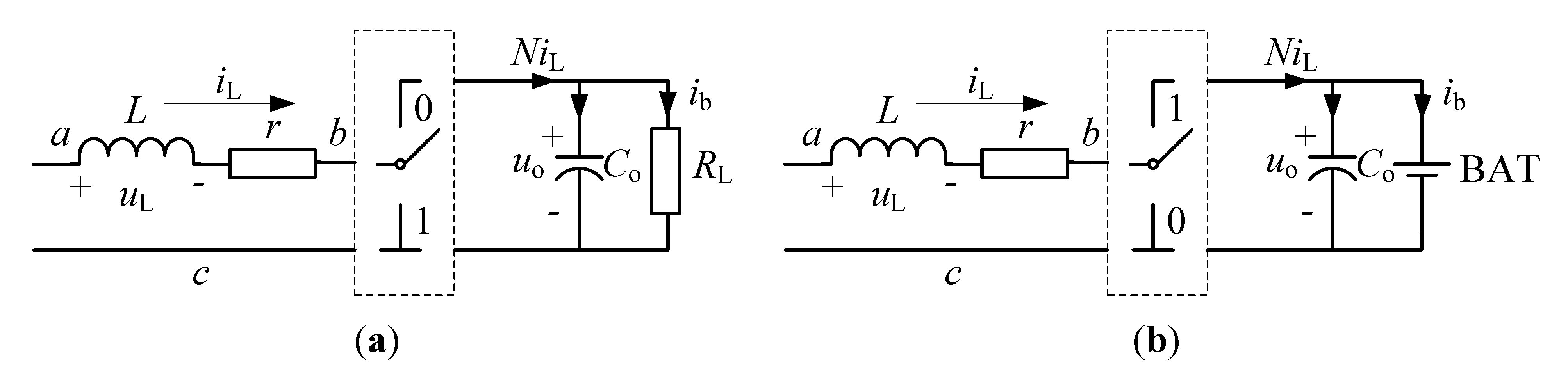
3.2.1. Charging Mode


3.2.2. Discharging Mode


3.3. Harmonic Characteristics Analysis
3.3.1. PWM Modulation of the Topology


3.3.2. Harmonic Analysis of Port Voltage ubc(t) of High-Frequency Switching Networks


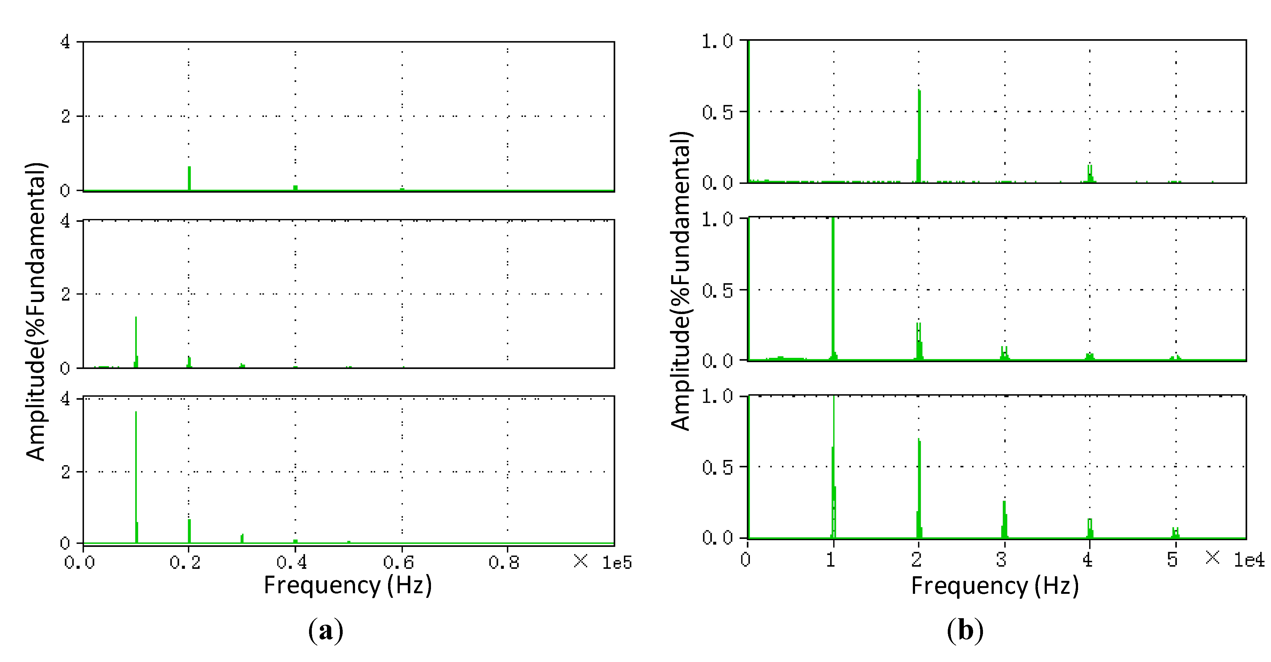
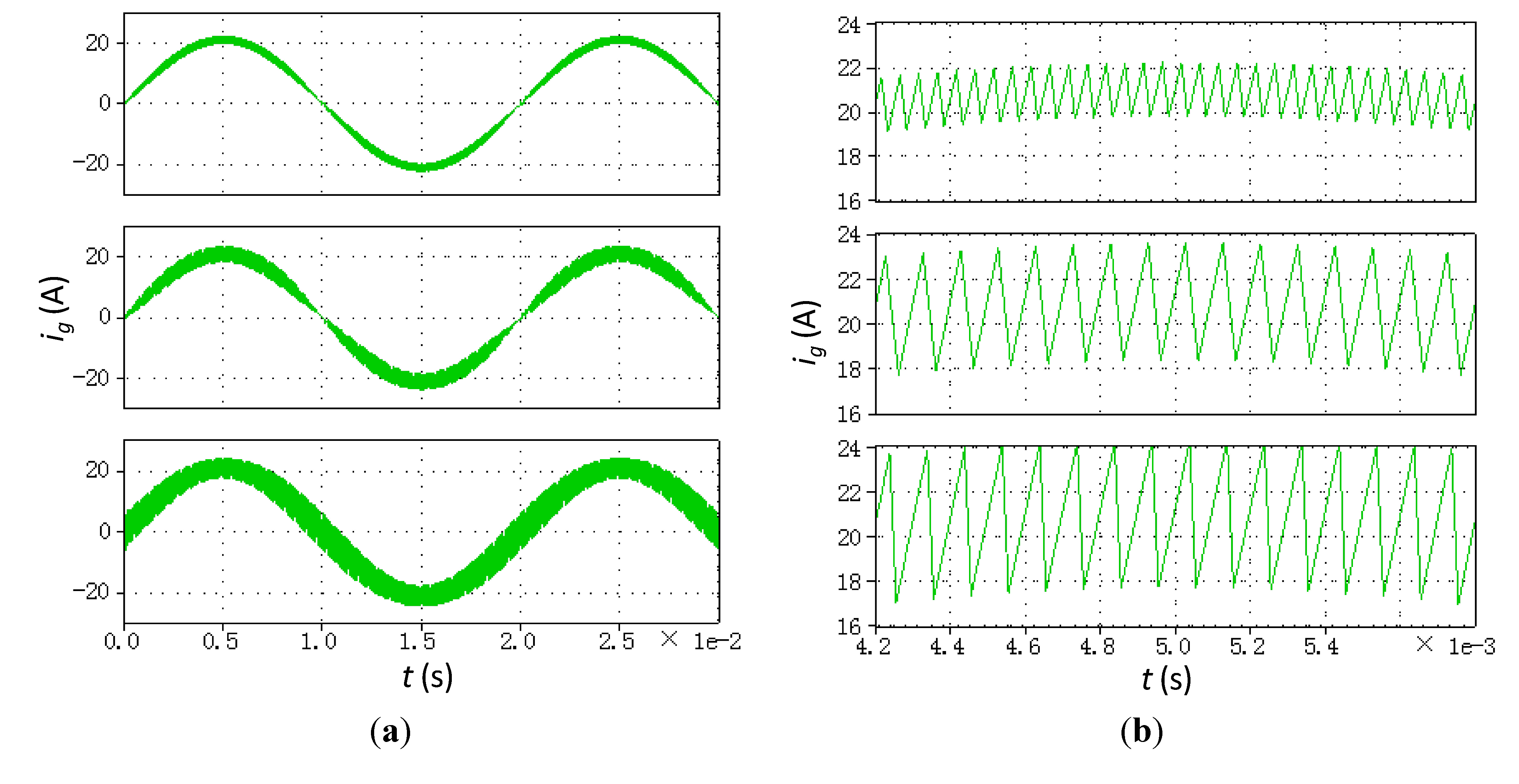
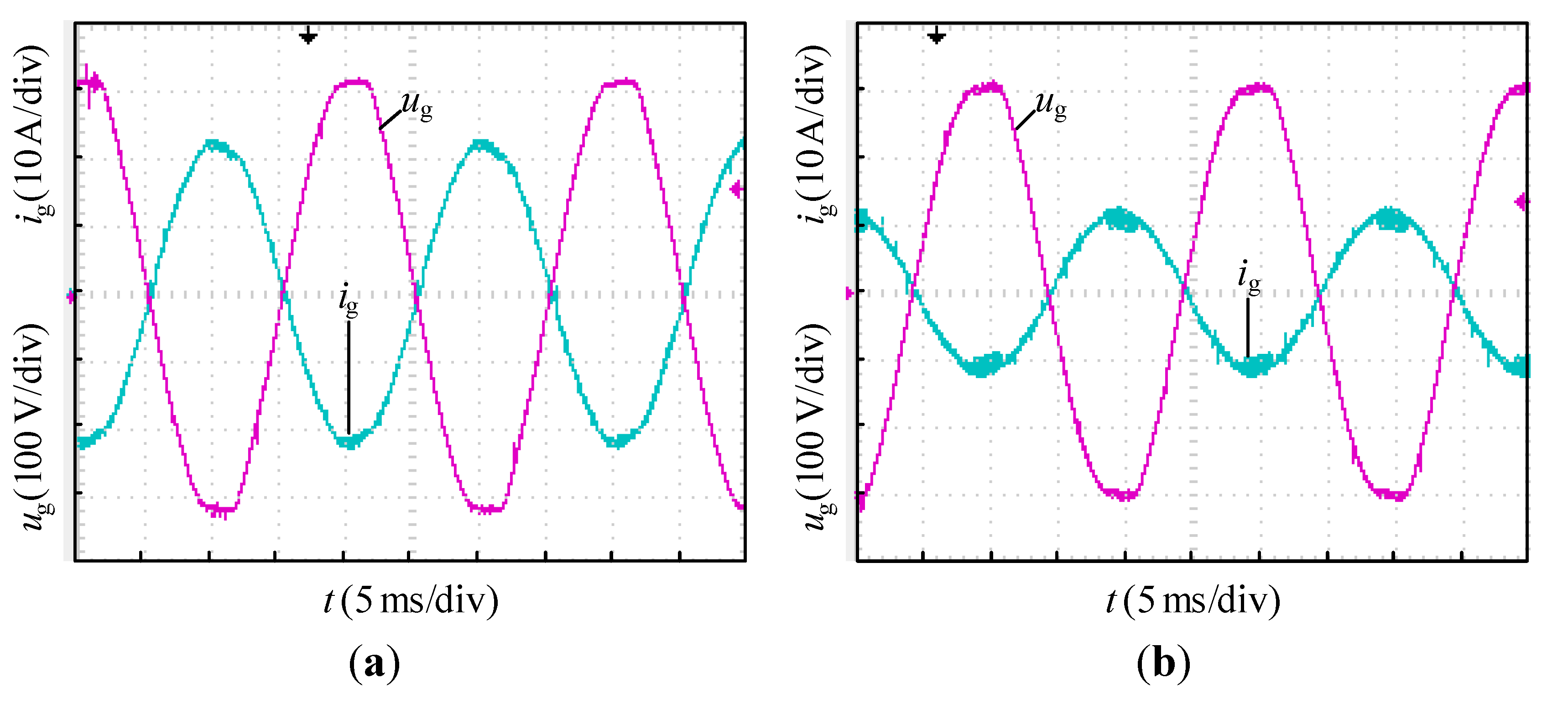
3.3.3. Harmonic Comparison and Analysis of Grid Current ig(t)


 . Substituting Equation (12) into Equation (11) and solving the new equation, we obtain:

 , where
  is the fundamental peak value of the grid current. Thus, the grid current in the unipolar modulation mode can be written as:


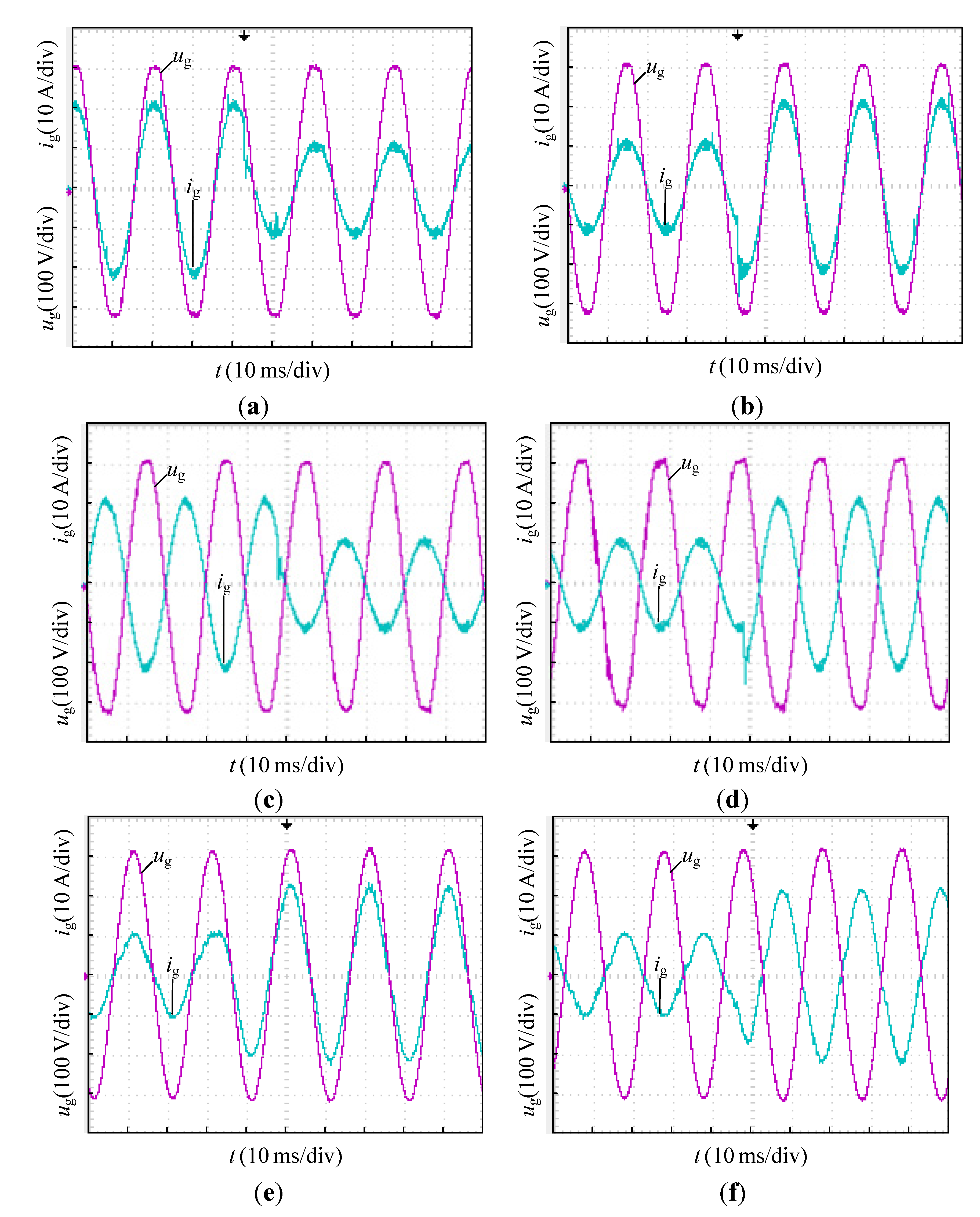
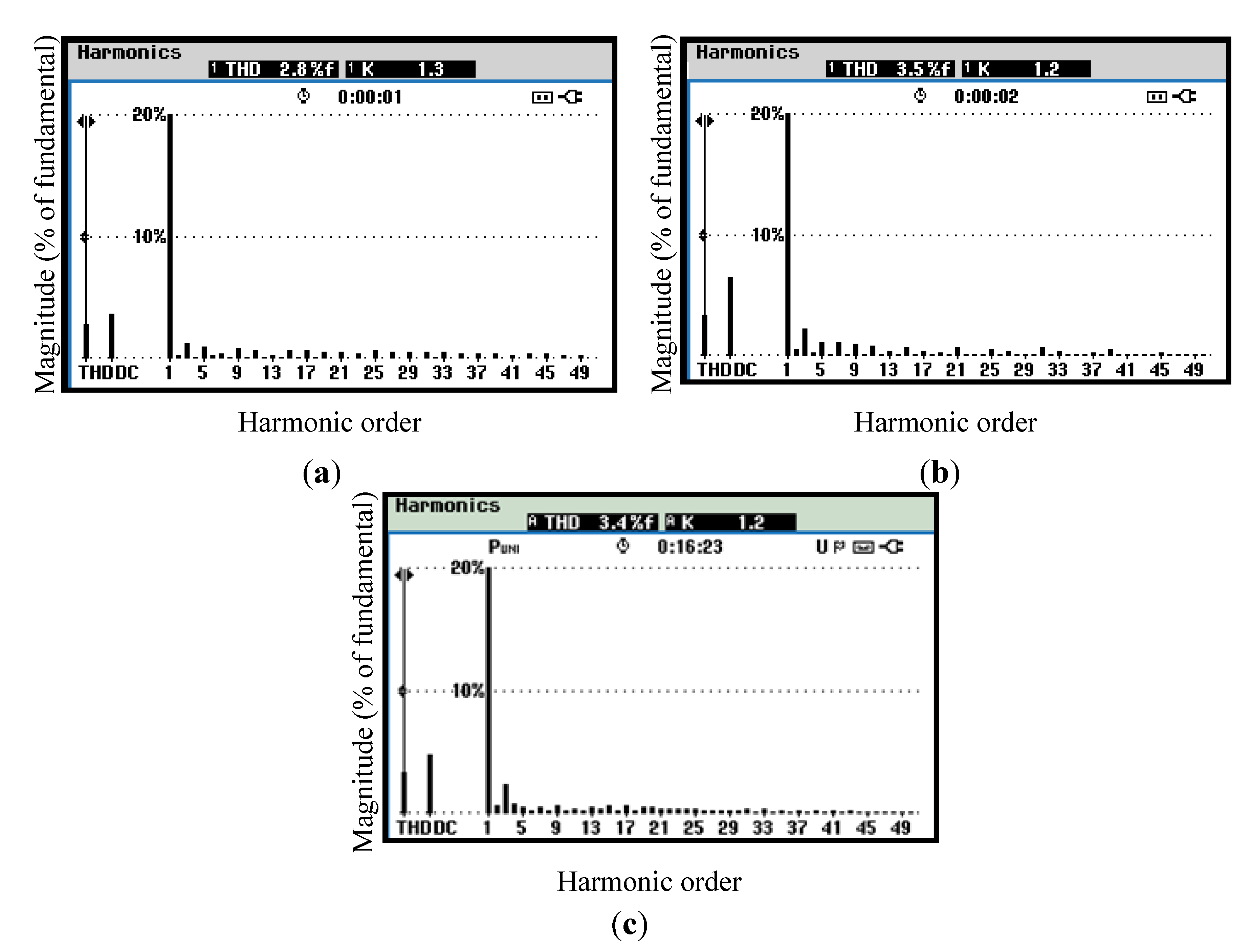
3.3.4. Verification of Harmonic Analysis of Grid Current ig(t)


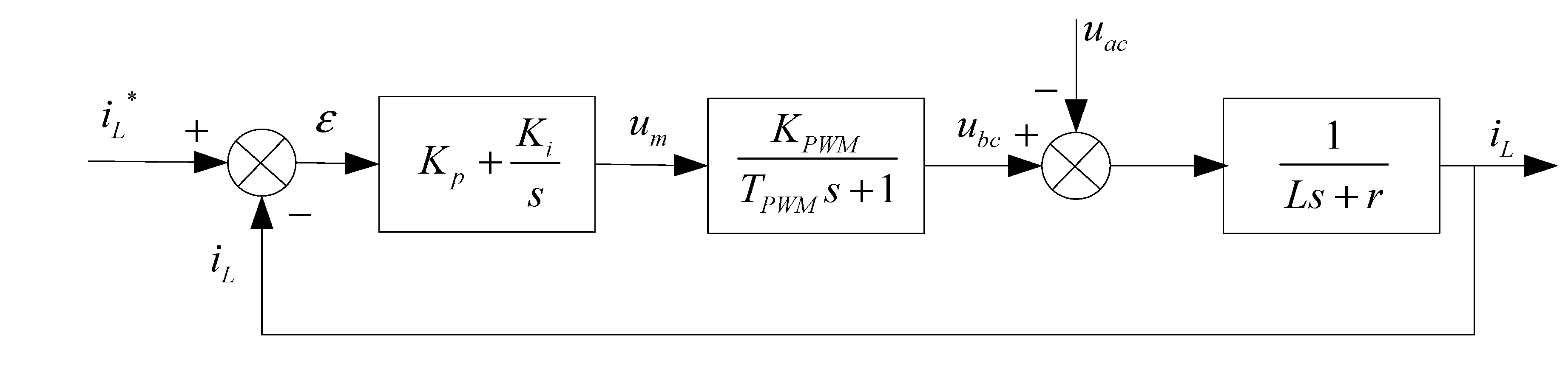
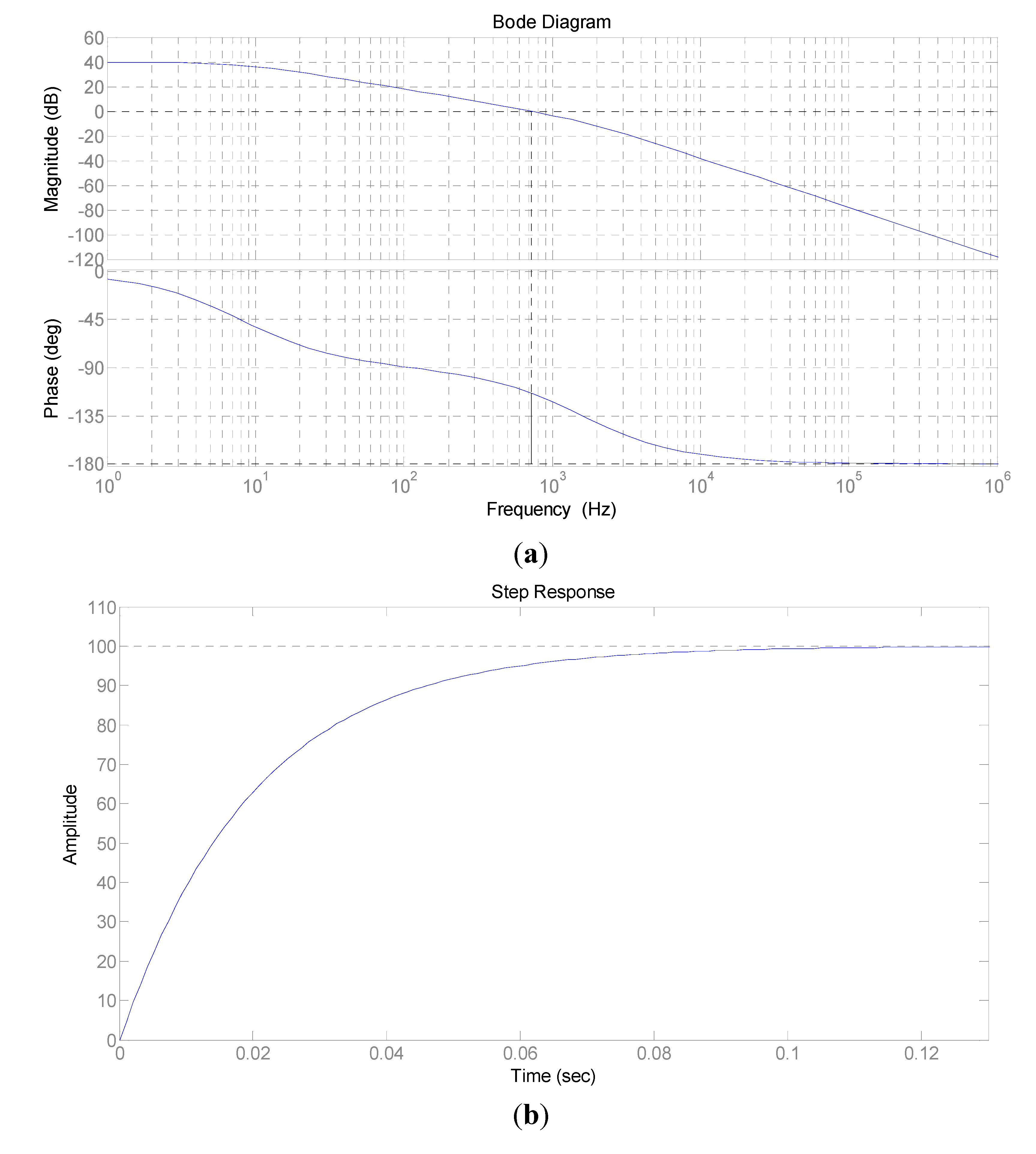
3.4. Dynamic Characteristics


 is the RMS value of the duty cycle in the line-frequency cycle, and uabrms is the RMS value of uab.
 , the load is a constant voltage source, and by high-frequency approximation, Equation (17) can be simplified to:


4. Design Considerations
4.1. High-Frequency Transformer

 is the minimum voltage of the battery pack, Dmin is the minimum duty cycle,
  is the maximum peak voltage of the grid considering the fluctuation range of the grid voltage. Since the BSS-FBC adopts PWM modulation, in order to guarantee its operation, the turn ratio of transformer also has to satisfy:

4.2. Filtering Inductor


4.3. Battery-Side Storage Capacitor

 in Cartesian coordinates in 0.01s period. If a 10% voltage ripple is considered, then the value of the capacitor should satisfy:

4.4. Dead-Time Capacitor

 is the voltage variation of the dead-time capacitor, ILd is the transient inductor current in the dead time.


5. Discussions
- (1)
- Higher Power Density, Reduced Component Count, Smaller Size, Lighter WeightOne of the major drawbacks of the typical two-stage bidirectional converters is the presence of the bulky DC intermediate link capacitor [39]. The proposed novel topology eliminates the bulky and expensive DC link capacitor. Furthermore, the inductor in the bidirectional DC-DC converter stage is no longer needed due to the current source nature of this topology. As a result, the component count, size and weight of the converter are reduced, leading to improved power density. These advantages are of importance in resolving the main challenges for on-board bidirectional converters in V2G applications.
- (2)
- Cost EffectivenessCost reduction has critical impact on realization of V2G. By eliminating the expensive DC link capacitors and special customized inductor from the typical two-stage topologies, the count of passive components is reduced significantly (there are only one inductor and one energy storage capacitor in the new topology). Accordingly, the cost of the bidirectional converter is reduced. Furthermore, all twelve active switches in the typical two-stage topologies operate under high voltage stress, whereas the switches S1–S4 in the new topology only operate under the grid voltage which is much lower than the voltages in the single-phase PWM converter who has the boost converter characteristic and the voltage stress of switches is equal to DC-side voltage of PWM converter. This lower voltage stress leads to lower grade active switches S1–S4, and hence much reduced cost.
- (3)
- Less HarmonicsThe PWM modulation mode of the BSS-FBC is similar to the unipolar modulation of the single-phase PWM converter. It has less harmonic components compared to the bipolar modulated single-phase PWM converter. Under the same inductance and switching frequency, the new topology has less harmonic components than unipolar modulated single-phase PWM converters.
- (4)
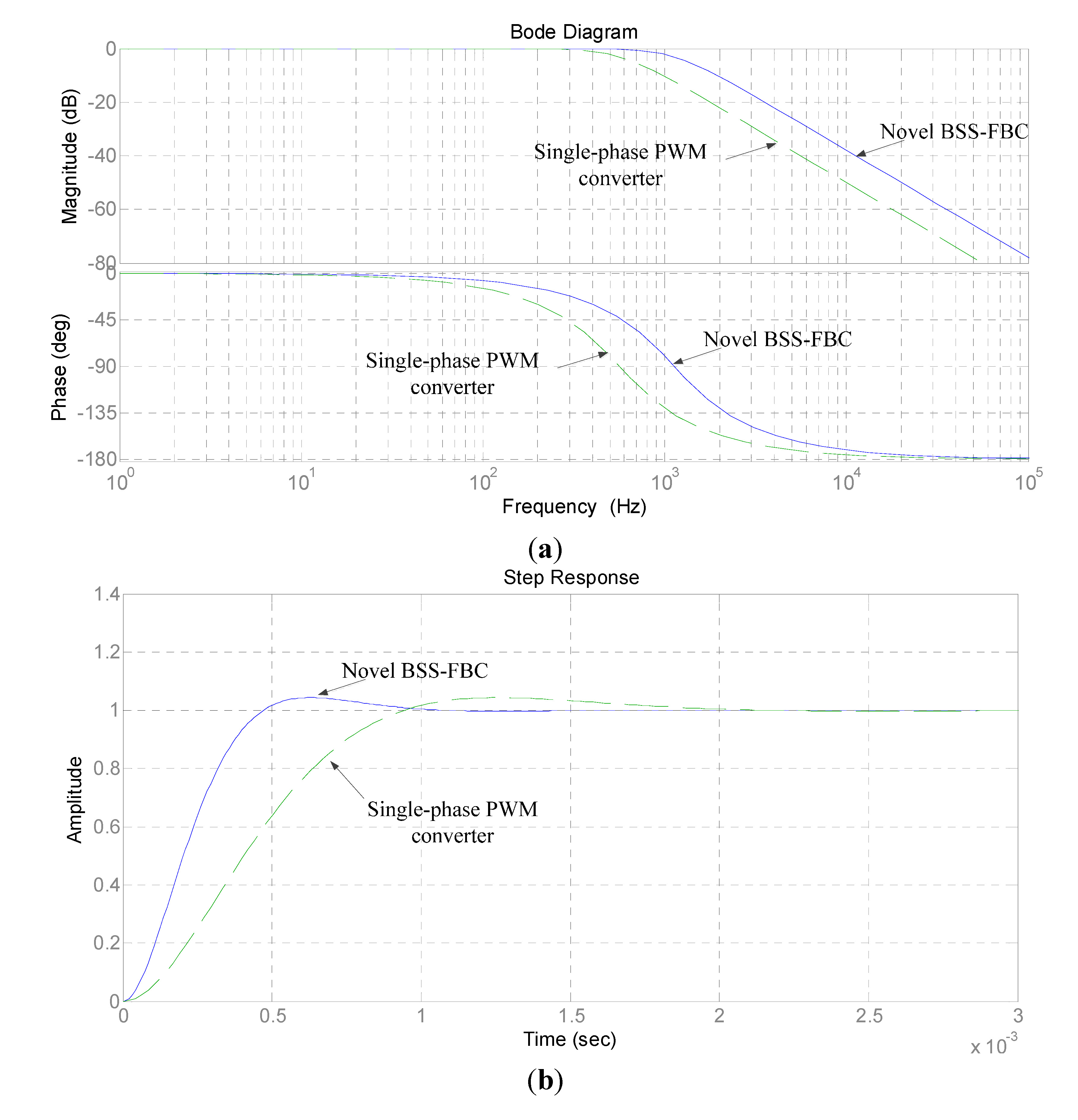
- Excellent Dynamic CharacteristicsAlso, from the analysis of harmonics, it can be seen that compared with two-stage topologies using PWM converters as the current shaping stage, with the same ripple factor and switching frequency, the value of the inductor L is smaller in the new topology. According to the control block diagram in Figure 17, the reduced value of the inductor will result in a positive effect on the dynamic characteristic. The response speed will be much faster since L acts as an inertia time constant in the control loop. With a suitable design of the compensators for the control loops, the dynamic characteristics of the new topology can outperform the typical converters.
- (5)
- High EfficiencyPower efficiency is a key performance index for converters and is especially important for their V2G applications. The proposed topology has the advantage of high efficiency for several reasons: First, it has less passive components, leading to reduced losses, such as copper loss and core loss of inductor. Second, lower voltage stress of the switches S1–S4 means lower conduction losses on them. Third, comparing to the bipolar and unipolar modulated single-phase PWM converters in typical two-stage topologies, the new topology has less harmonic components and smaller inductor current ripples. This will reduce losses, EMI, and the size of inductor L to a certain extent. Fourth, only four active switches in the new topology operate in high frequency, regardless if it is in the charging or discharging mode. In contrast, all twelve switches of typical two-stage topologies operate in high frequency, causing additional switching losses. Finally, the four switches S1–S4 in the new topology turn on and off at the zero-crossing point of the grid voltage and current and have no switching losses. We observe that although some switches in the DC-DC conversion stage of typical topologies realize soft-switching, they do not achieve this at the same switching time and soft-switching cannot be guaranteed during load changes or wide-range power flow variations.
- (6)
- Increased Reliability, Simpler Control, and Reduced ComplexityElectrolytic capacitors used in DC intermediate links of two-stage topologies are likely to reduce converter reliability with their limited lifecycles. By eliminating this capacitor, the new topology can potentially enhance reliability. Usually, the grid-side current shaping stage and DC-DC conversion stage of typical two-stage converters are controlled separately by two micro control units using different control strategies. The new topology combines the two functions in one stage and only has four active switches to be PWM controlled (the switches S1–S4 are uncontrolled or driven by line-frequency pulses with constant duty cycle which don’t need any active control). As a result, it uses only one micro control unit. Without loop interactions, the control design is also much simplified. As a result, the reliability is increased due to the simple control design and implementation and reduced sensors.
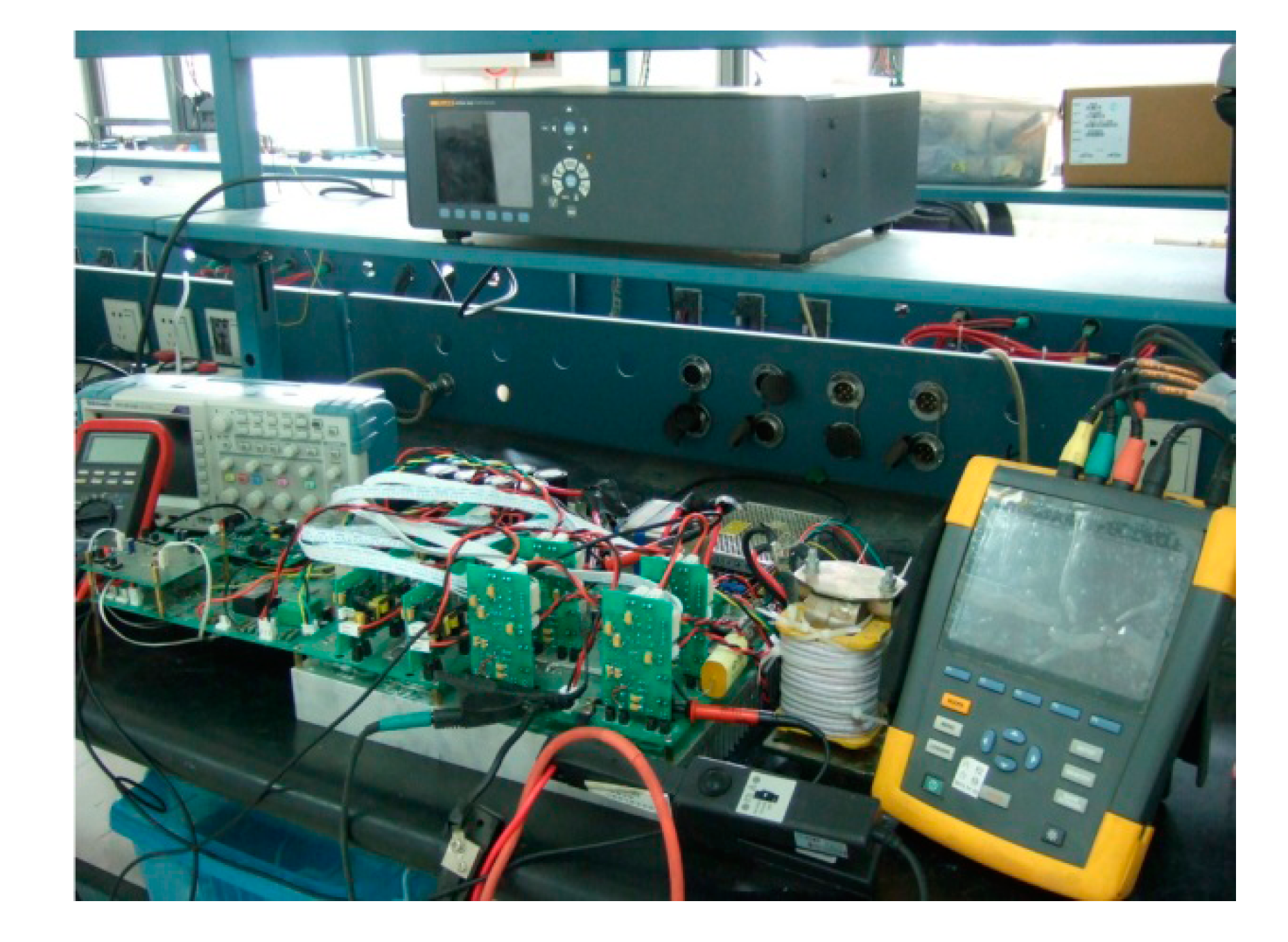
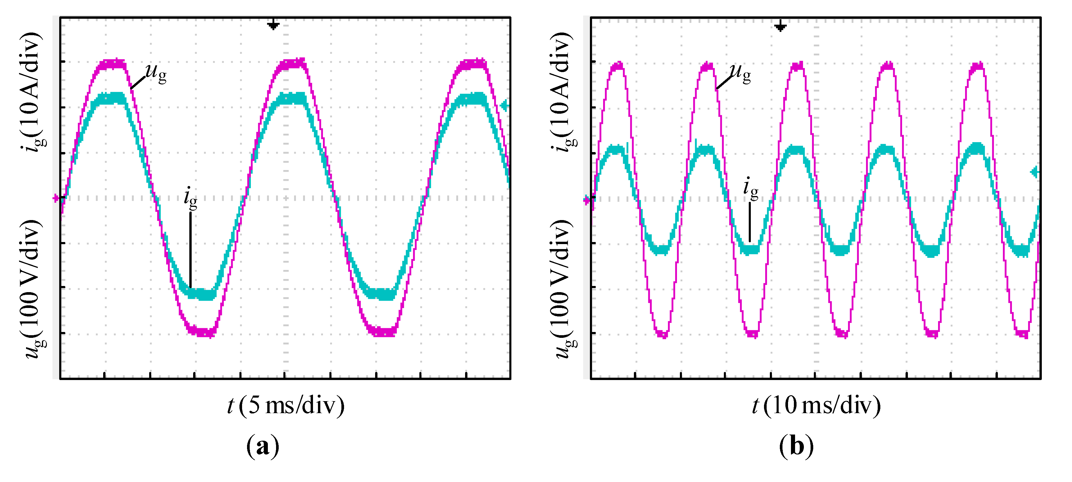
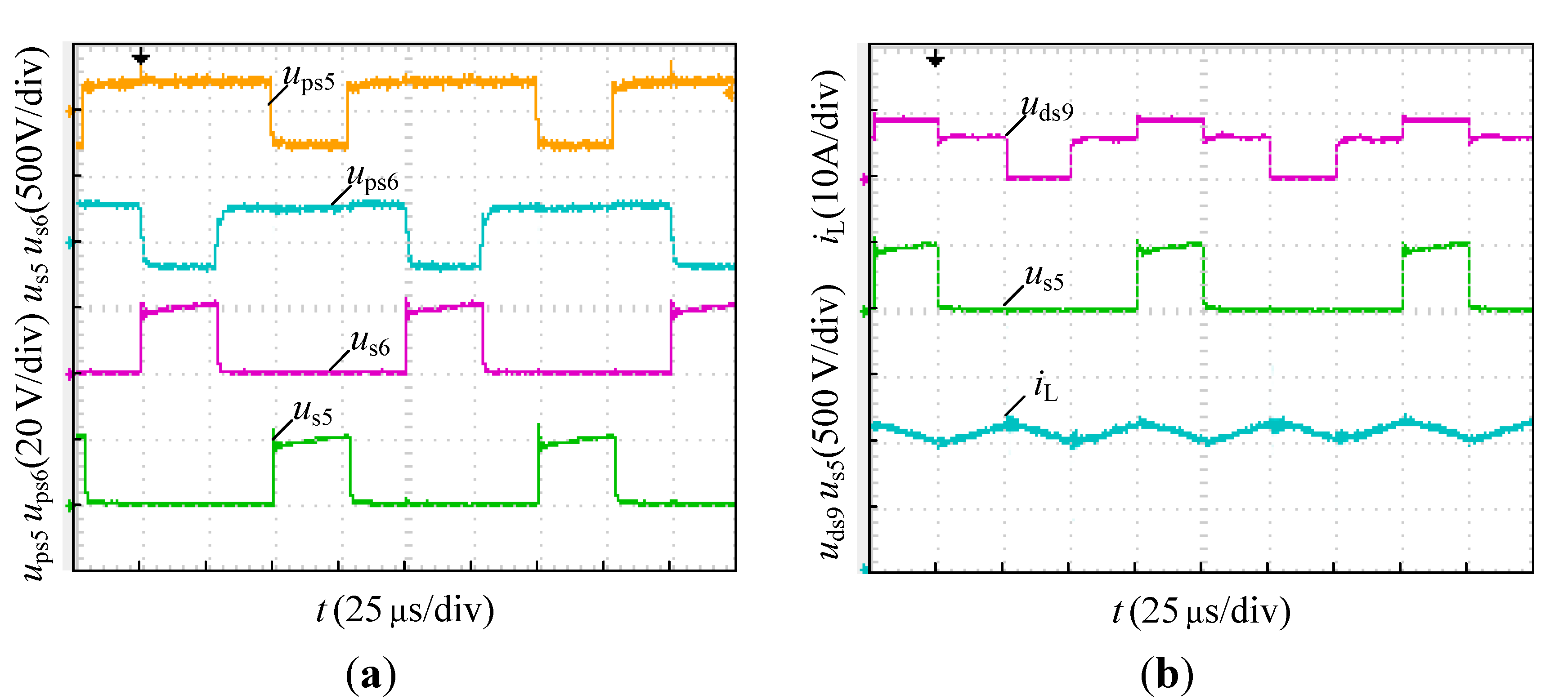
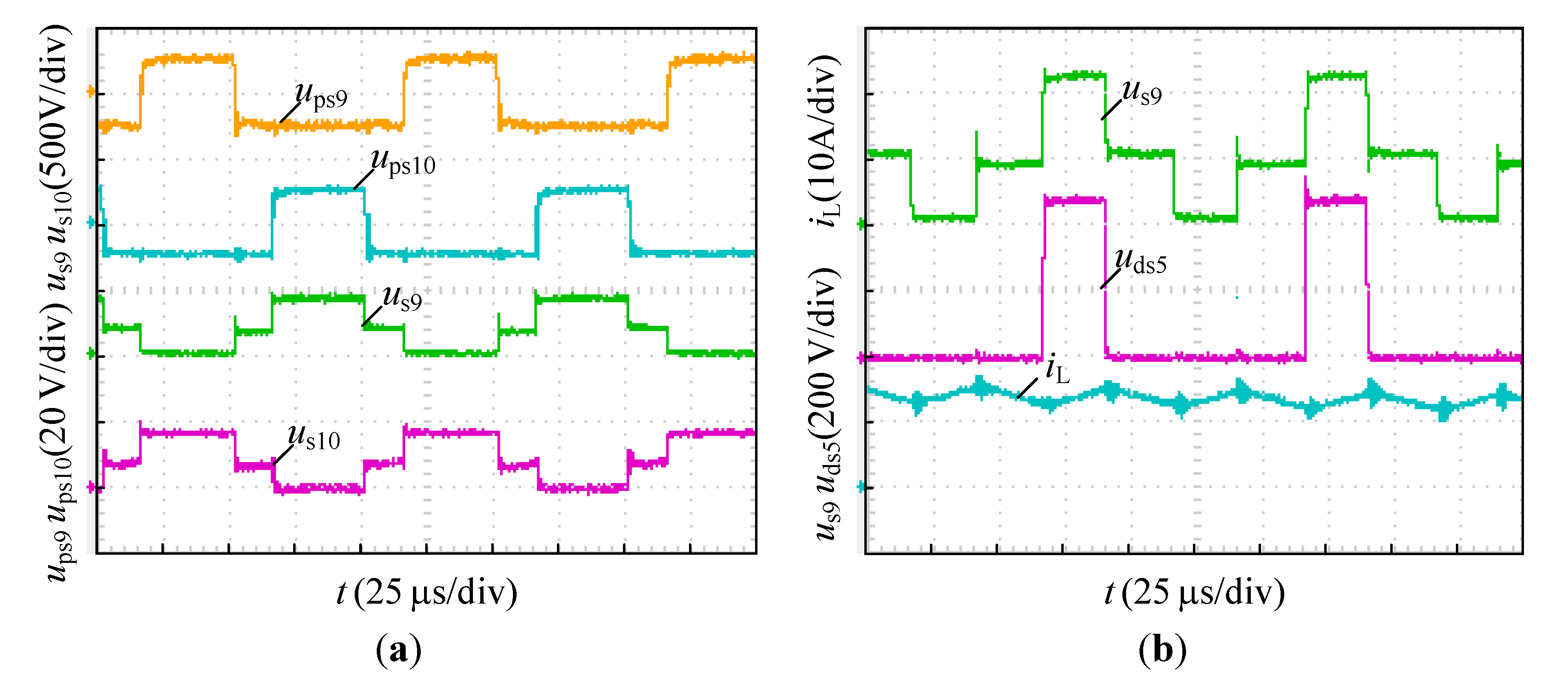
6. Experimental Results
6.1. Specifications

| Parameters | Value | Unit |
|---|---|---|
| Nominal Power | 3300 | W |
| AC Grid Voltage (RMS) | 220 ± 10% | V |
| AC Grid Frequency | 50 | Hz |
| Battery DC Voltage | 336 to 444 | V |
| Switching Frequency of Active Switches | 10 | kHz |
| Inductor | 2 | mH |
| Energy Storage Capacitor | 4000 | μF |
| Turn Ratio of Transformer | 1.1 | - |
| Dead-time Capacitor | 3 | μF |
| Dead Time | 0.5 | μs |
6.2. Experimental Results


| Power (% PN) | Charging Ib (A) | Discharging ig_rms(A) | Charging Efficiency | Discharging Efficiency |
|---|---|---|---|---|
| 100% | 7.4 | 15 | 92.7% | 94.2% |
| 75% | 5.6 | 11.3 | 94.6% | 95.7% |
| 50% | 3.7 | 7.5 | 94.9% | 95.4% |
| 30% | 2.2 | 4.5 | 91.8% | 92.4% |
7. Conclusions
Acknowledgments
Author Contributions
Conflicts of Interest
References
- Amin, S.M.; Wollenberg, B.F. Toward a smart grid: Power delivery for the 21st century. IEEE Power Energy Mag. 2005, 3, 34–41. [Google Scholar]
- Ipakchi, A.; Albuyeh, F. Grid of the future. IEEE Power Energy Mag. 2009, 7, 52–62. [Google Scholar] [CrossRef]
- Chan, C.C. The state of the art of electric and hybrid vehicles. Proc. IEEE 2002, 90, 247–275. [Google Scholar]
- Chan, C.C. The state of the art of electric, hybrid, and fuel cell vehicles. Proc. IEEE 2007, 95, 704–718. [Google Scholar] [CrossRef]
- Clement-Nyns, K.; Haesen, E.; Driesen, J. The impact of charging plug-in hybrid electric vehicles on a residential distribution grid. IEEE Trans. Power Syst. 2010, 25, 371–380. [Google Scholar]
- Lopes, J.A.P.; Soares, F.J.; Almeida, P.M.R. Integration of electric vehicles in the electric power system. Proc. IEEE 2011, 99, 168–183. [Google Scholar] [CrossRef]
- Kempton, W.; Letendre, S.E. Electric vehicles as a new power source for electric utilities. Transp. Res. Part D 1997, 2, 157–175. [Google Scholar] [CrossRef]
- Kempton, W.; Tomić, J. Vehicle-to-grid power fundamentals: Calculating capacity and net revenue. J. Power Sources 2005, 144, 268–279. [Google Scholar] [CrossRef]
- Kempton, W.; Tomić, J. Vehicle-to-grid power implementation: From stabilizing the grid to supporting large-scale renewable energy. J. Power Sources 2005, 144, 280–294. [Google Scholar] [CrossRef]
- Tomić, J.; Kempton, W. Using fleets of electric-drive vehicles for grid support. J. Power Sources 2007, 168, 459–468. [Google Scholar]
- Clement-Nyns, K.; Haesen, E.; Driesen, J. The impact of vehicle-to-grid on the distribution grid. Electric Power Syst. Res. 2011, 81, 185–192. [Google Scholar]
- Yu, Y.F.; Zhang, Q.F.; Liang, B.; Liu, X.F.; Cui, S.M. Analysis of a single-phase Z-source inverter for battery discharging in vehicle to grid applications. Energies 2011, 4, 2224–2235. [Google Scholar] [CrossRef]
- Jian, L.N.; Xue, H.H.; Xu, G.Q.; Zhu, X.Y.; Zhao, D.F.; Shao, Z.Y. Regulated charging of plug-in hybrid electric vehicles for minimizing load variance in household smart microgrid. IEEE Trans. Ind. Electron. 2013, 60, 3218–3226. [Google Scholar] [CrossRef]
- Luo, Z.W.; Hu, Z.C.; Song, Y.H.; Xu, Z.W.; Lu, H.Y. Optimal coordination of plug-in electric vehicles in power grids with cost-benefit analysis—Part I: Enabling techniques. IEEE Trans. Power Syst. 2013, 28, 3546–3555. [Google Scholar] [CrossRef]
- Luo, Z.W.; Hu, Z.C.; Song, Y.H.; Xu, Z.W.; Lu, H.Y. Optimal coordination of plug-in electric vehicles in power grids with cost-benefit analysis—Part II: A case study in China. IEEE Trans. Power Syst. 2013, 28, 3556–3565. [Google Scholar] [CrossRef]
- Wang, Z.P.; Wang, S. Grid power peak shaving and valley filling using vehicle-to-grid systems. IEEE Trans. Power Deliver. 2013, 28, 1822–1829. [Google Scholar] [CrossRef]
- Soares, J.; Morais, H.; Sousa, T.; Vale, Z.; Faria, P. Day-ahead resource scheduling including demand response for electric vehicles. IEEE Trans. Smart Grid 2013, 4, 596–605. [Google Scholar] [CrossRef]
- Yao, W.F.; Zhao, J.H.; Wen, F.S.; Xue, Y.S.; Ledwich, G. A hierarchical decomposition approach for coordinated dispatch of plug-in electric vehicles. IEEE Trans. Power Syst. 2013, 28, 2678–2778. [Google Scholar] [CrossRef]
- Mu, Y.F.; Wu, J.Z.; Ekanayake, J.; Jenkins, N.; Jia, H.J. Primary frequency response from electric vehicles in the great britain power system. IEEE Trans. Smart Grid 2013, 4, 1142–1150. [Google Scholar] [CrossRef]
- Geng, B.; Mills, J.K.; Sun, D. Two-stage charging strategy for plug-in electric vehicles at the residential transformer level. IEEE Trans. Smart Grid 2013, 4, 1442–1452. [Google Scholar] [CrossRef]
- Hu, W.H.; Su, C.; Chen, Z.; Bak-Jensen, B. Optimal operation of plug-in electric vehicles in power systems with high wind power penetrations. IEEE Trans. Sustain. Energy 2013, 4, 577–585. [Google Scholar] [CrossRef]
- Singh, M.; Kumar, P.; Kar, I. A multi charging station for electric vehicles and its utilization for load management and the grid support. IEEE Trans. Smart Grid 2013, 4, 1026–1037. [Google Scholar] [CrossRef]
- Mohamed, A.; Salehi, V.; Ma, T.; Mohamed, O.A. Real-time energy management algorithm for plug-in hybrid electric vehicle charging parks involving sustainable energy. IEEE Trans. Sustain. Energy 2014, 5, 577–586. [Google Scholar] [CrossRef]
- Singh, M.; Thirugnanam, K.; Kumar, P.; Kar, I. Real-time coordination of electric vehicles to support the grid at the distribution substation level. IEEE Syst. J. 2013, PP, 1–11. [Google Scholar] [CrossRef]
- Chukwu, U.C.; Mahajan, S.M. Real-time management of power systems with V2G facility for smart-grid applications. IEEE Trans. Sustain. Energy 2014, 5, 558–566. [Google Scholar] [CrossRef]
- Sun, S.; Dong, M.; Liang, B. Real-time welfare-maximizing regulation allocation in dynamic aggregator-EVs system. IEEE Trans. Smart Grid 2014, 5, 1397–1409. [Google Scholar] [CrossRef]
- Kennel, F.; Gorges, D.; Liu, S. Energy management for smart grids with electric vehicles based on hierarchical MPC. IEEE Trans. Ind. Inf. 2013, 9, 1528–1537. [Google Scholar] [CrossRef]
- Gao, S.; Chau, K.T.; Liu, C.H.; Wu, D.Y.; Chan, C.C. Integrated energy management of plug-in electric vehicles in power grid with renewables. IEEE Trans. Veh. Technol. 2014, PP, 1–8. [Google Scholar] [CrossRef]
- Liu, H.; Hu, Z.C.; Song, Y.H.; Lin, J. Decentralized vehicle-to-grid control for primary frequency regulation considering charging demands. IEEE Trans. Power Syst. 2013, 28, 3480–3489. [Google Scholar] [CrossRef]
- Vachirasricirikul, S.; Ngamroo, I. Robust LFC in a smart grid with wind power penetration by coordinated V2G control and frequency controller. IEEE Trans. Smart Grid 2014, 5, 371–380. [Google Scholar] [CrossRef]
- Thirugnanam, K.; Joy, T.P.; Singh, M.; Kumar, P. Mathematical modeling of Li-Ion battery using genetic algorithm approach for V2G applications. IEEE Trans. on Energy Conver. 2014, 29, 332–343. [Google Scholar] [CrossRef]
- Landi, M.; Gross, G. Measurement techniques for online battery state of health estimation in vehicle-to-grid applications. IEEE Trans. Instrum. Meas. 2014, 63, 1224–1234. [Google Scholar] [CrossRef]
- Ustun, T.S.; Ozansoy, C.R.; Zayegh, A. Implementing vehicle-to-grid (V2G) technology with IEC 61850-7-420. IEEE Trans. Smart Grid 2013, 4, 1180–1187. [Google Scholar] [CrossRef]
- Xu, D.Q.; Joós, G.; Lévesque, M.; Maier, M. Integrated V2G, G2V, and renewable energy sources coordination over a converged fiber-wireless broadband access network. IEEE Trans. Smart Grid 2013, 4, 1381–1390. [Google Scholar] [CrossRef]
- Liu, H.; Ning, H.S.; Zhang, Y.; Xiong, Q.X.; Yang, L.T. Role-dependent privacy preservation for secure V2G networks in the smart grid. IEEE Trans. Inf. Forens. Secur. 2014, 9, 208–220. [Google Scholar] [CrossRef]
- NIST Framework and Roadmap for Smart Grid Interoperability Standards; National Institute of Standards and Technology: Gaithersburg, MD, USA, 2010.
- Yilmaz, M.; Krein, P.T. Review of battery charger topologies, charging power levels, and infrastructure for plug-in electric and hybrid vehicles. IEEE Trans. Power Electron. 2013, 28, 2151–2169. [Google Scholar] [CrossRef]
- Inoue, S.; Akagi, H. A bidirectional DC/DC converter for an energy storage system with galvanic isolation. IEEE Trans. Power Electron. 2007, 22, 2299–2306. [Google Scholar] [CrossRef]
- Khaligh, A.; Dusmez, S. Comprehensive topological analysis of conductive and inductive charging solutions for plug-in electric vehicles. IEEE Trans. Veh. Technol. 2012, 61, 3475–3489. [Google Scholar] [CrossRef]
- Haghbin, S.; Lundmark, S.; Alaküla, M.; Carlson, O. Grid-connected integrated battery chargers in vehicle applications: Review and new solution. IEEE Trans. Ind. Electron. 2013, 60, 459–473. [Google Scholar] [CrossRef]
- Haghbin, S.; Khan, K.; Lundmark, S.; Alaküla, M.; Carlson, O.; Leksell, M.; Wallmark, O. Integrated chargers for EV’s and PHEV’s: Examples and new solutions. In Proceedings of the 2010 XIX International Conference on Electrical Machines,, Rome, Italy, 6–8 September 2010; pp. 1–6.
- Bruyère, A.; Sousa, L.D.; Bouchez, B.; Sandulescu, P.; Kestelyn, X.; Semail, E. A multiphase traction/fast-battery-charger drive for electric or plug-in hybrid vehicles: Solutions for control in traction mode. In Proceedings of the 2010 IEEE Vehicle Power and Propulsion Conference (VPPC), Lille, France, 1–3 September 2010; pp. 1–7.
- Lacroix, S.; Laboure, E.; Hilairet, M. An integrated fast battery charger for electric vehicle. In Proceedings of the 2010 IEEE Vehicle Power and Propulsion Conference (VPPC), Lille, France, 1–3 September 2010; pp. 1–6.
- Sousa, L.D.; Silvestre, B.; Bouchez, B. A combined multiphase electric drive and fast battery charger for electric vehicles. In Proceedings of the 2010 IEEE Vehicle Power and Propulsion Conference (VPPC), Lille, France, 1–3 September 2010; pp. 1–6.
- Haghbin, S.; Alaküla, M.; Khan, K.; Lundmark, S.; Leksell, M.; Wallmark, O.; Carlson, O. An integrated charger for plug-in hybrid electric vehicles based on a special interior permanent magnet motor. In Proceedings of the 2010 IEEE Vehicle Power and Propulsion Conference (VPPC), Lille, France, 1–3 September 2010; pp. 1–6.
- Rodrigues, M.C.B.P.; Souza, I.; Ferreira, A.A.; Barbosa, P.G.; Braga, H.A.C. Integrated bidirectional single-phase vehicle-to-grid interface with active power filter capability. In Proceedings of 2013 Brazilian Power Electronics Conference (COBEP), Gramado, Brazil, 27–31 October 2013; pp. 993–1000.
- Khan, M.A.; Husain, I.; Sozer, Y. Integrated electric motor drive and power electronics for bidirectional power flow between the electric vehicle and DC or AC grid. IEEE Trans. Power Electron. 2013, 28, 5774–5783. [Google Scholar] [CrossRef]
- Haghbin, S.; Khan, K.; Shuang, Z.; Alakula, M.; Lundmark, S.; Carlson, O. An integrated 20-kW motor drive and isolated battery charger for plug-in vehicles. IEEE Trans. Power Electron. 2013, 28, 4013–4029. [Google Scholar] [CrossRef]
- IEEE Standard for Interconnecting Distributed Resources with Electric Power Systems; The Institute of Electrical and Electronics Engineers: New York, NY, USA, 2003.
- Electromagnetic Compatibility (EMC)—Part 3-2: Limits—Limits for Harmonic Current Emissions (Equipment Input Current ≤ 16 A per Phase); International Electrotechnical Commission: Geneva, Switzerland, 2000.
- Jarnut, M.; Benysek, G. Application of power electronics devices in smart grid and V2G (vehicle to grid) technologies. Prz. Elektrotech. 2010, 86, 93–96. [Google Scholar]
- Kisacikoglu, M.C.; Ozpineci, B.; Tolbert, L.M. Effects of V2G reactive power compensation on the component selection in an EV or PHEV bidirectional charger. In Proceedings of the IEEE Energy Conversion Congress and Exposition (ECCE), Atlanta, GA, USA, 12–16 September 2010; pp. 870–876.
- Pinto, J.G.; Monteiro, V.; Gonçalves, H.; Afonso, J.L. Onboard reconfigurable battery charger for electric vehicles with traction-to-auxiliary mode. IEEE Trans. Veh. Technol. 2014, 63, 1104–1116. [Google Scholar] [CrossRef] [Green Version]
- Pinto, J.G.; Monteiro, V.; Goncalves, H.; Exposto, B.; Pedrosa, D.; Couto, C.; Afonso, J.L. Bidirectional battery charger with Grid-to-Vehicle, Vehicle-to-Grid and Vehicle-to-Home technologies. In Proceedings of the 39th Annual Conference of the IEEE Industrial Electronics Society, IECON 2013, Vienna, Austria, 10–13 November 2013; pp. 5934–5939.
- Khan, M.A.; Husain, I.; Sozer, Y. A bi-directional DC-DC converter with overlapping input and output voltage ranges and vehicle to grid energy transfer capability. In Proceedings of 2012 IEEE International Electric Vehicle Conference (IEVC), Greenville, CA, USA, 4–8 March 2012; pp. 1–7.
- Hegazy, O.; Barrero, R.; Mierlo, J.V.; Lataire, P.; Omar, N.; Coosemans, T. An advanced power electronics interface for electric vehicles applications. IEEE Trans. Power Electron. 2013, 28, 5508–5521. [Google Scholar] [CrossRef]
- Wong, N.; Kazerani, M. A review of bidirectional on-board chargertopologies for plugin vehicles. In Proceedings of the 25th IEEE Canadian Conference on Electrical & Computer Engineering (CCECE), Montreal, Canada, 29 April–2 May 2012; pp. 1–6.
- De Doncker, R.W.A.A.; Divan, D.M.; Kheraluwala, M.H. A three-phase soft-switched high-power-density DC/DC converter for high-power applications. IEEE Trans. Ind. Appl. 1991, 27, 63–73. [Google Scholar]
- Xie, Y.H.; Sun, J.; Freudenberg, J.S. Power flow characterization of a bidirectional galvanically isolated high-power DC/DC converter over a wide operating range. IEEE Trans. Power Electron. 2010, 25, 54–66. [Google Scholar] [CrossRef]
- Shi, X.L.; Jiang, J.C.; Guo, X.T. An efficiency-optimized isolated bidirectional DC-DC converter with extended power range for energy storage systems in microgrids. Energies 2013, 6, 27–44. [Google Scholar] [CrossRef]
- Kanaan, H.Y.; Caron, M.; Al-Haddad, K. Design and implementation of a two-stage grid-connected high efficiency power load emulator. IEEE Trans. Power Electron. 2014, 29, 3997–4006. [Google Scholar] [CrossRef]
- Zhao, B.; Song, Q.; Liu, W.H.; Sun, Y.D. Overview of dual-active bridge isolated bidirectional dc-dc converter for high frequency-link power-conversion system. IEEE Trans. Power Electron. 2014, 29, 4091–4106. [Google Scholar] [CrossRef]
- Pan, X.; Rathore, A.K. Novel bidirectional snubberless naturally commutated soft-switching current-fed full-bridge isolated DC/DC converter for fuel cell vehicles. IEEE Trans. Ind. Electron. 2014, 61, 2307–2315. [Google Scholar] [CrossRef]
- Li, X.D.; Bhat, A.K.S. Analysis and design of high-frequency isolated dual-bridge series resonant DC/DC converter. IEEE Trans. Power Electron. 2010, 25, 850–862. [Google Scholar] [CrossRef]
- Ebrahimi, S.; Taghavi, M.; Tahami, F.; Oraee, H. Integrated bidirectional isolated soft-switched battery charger for vehicle-to-grid technology using4-Switch 3Φ-rectifier. In Proceedings of the 39th Annual Conference of the IEEE Industrial Electronics Society, IECON 2013, Vienna, Austria, 10–13 November 2013; pp. 906–911.
- Madawala, U.K.; Thrimawithana, D.J. A bidirectional inductive power interface for electric vehicles in V2G systems. IEEE Trans. Ind. Electron. 2011, 58, 4789–4796. [Google Scholar] [CrossRef]
- Thrimawithana, D.J.; Madawala, U.K. A novel matrix converter based bi-directional IPT power interface for V2G applications. In Proceedings of the IEEE International Energy Conference and Exhibition (EnergyCon), Manama, Bahrain, 18–22 December 2010; pp. 495–500.
- Weise, N.D.; Gastelino, G.; Basu, K.; Mohan, N. A single-stage dual-active-bridge-based soft switched AC–DC converter with open-loop power. IEEE Trans. Power Electron. 2014, 29, 4007–4016. [Google Scholar] [CrossRef]
- Reimensnyder, N.; Weise, N. Voltage control of a single phase, single-stage, isolated AC-DC converter. In Proceedings of the IEEE Transportation Electrification Conference and Expo (ITEC), Detroit, MI, USA, 16–19 June 2013; pp. 1–5.
- Varajao, D.; Araujo, R.E.; Moreira, C.; Lopes, J.P. Impact of phase-shift modulation on the performance of a single-stage bidirectional electric vehicle charger. In Proceedings of the 38th Annual Conference on IEEE Industrial Electronics Society, Montreal, QC, Canada, 25–28 October 2012; pp. 5215–5220.
- Sanjaya, M. Switching Power Supply Design and Optimization; McGraw-Hill: New York, NY, USA, 2005; pp. 92–95. [Google Scholar]
- IEEE Recommended Practices and Requirements for Harmonic Control in Electrical Power Systems; The Institute of Electrical and Electronics Engineers: New York, NY, USA, 1993.
- Holmes, D.G.; Lipo, T.A. Pulse Width Modulation for Power Converters: Principles and Practice; IEEE Press: Piscataway, NJ, USA, 2003; pp. 155–211. [Google Scholar]
- Sekyung, H.; Soohee, H.; Sezaki, K. Development of an optimal vehicle-to-grid aggregator for frequency regulation. IEEE Trans. Smart Grid 2010, 1, 65–72. [Google Scholar] [CrossRef]
- Huliehel, F.A.; Lee, F.C.; Cho, B.H. Small-signal modeling of the single-phase boost high power factor converter with constant frequency control. In Proceedings of the 23rd Annual IEEE Power Electronics Specialists Conference, Toledo, OH, USA, 29 June–3 July 1992; pp. 475–482.
- Xie, M.J.; Lu, B.; Dong, W.; Lee, F.C. Novel current-loop feed-forward compensation for boost PFC converter. In Proceedings of the IEEE 19th Annual IEEE Applied Power Electronics Conference and Exposition, Anaheim, CA, USA, 22–26 February 2004; pp. 750–775.
- Hang, L.J.; Yao, W.X.; Lu, Z.Y.; Qian, Z.M.; Guerrero, J.M. Analysis of flux density bias and digital suppression strategy for single-stage power factor corrector converter. IEEE Trans. Ind. Electron. 2008, 55, 3077–3087. [Google Scholar] [CrossRef]
© 2014 by the authors; licensee MDPI, Basel, Switzerland. This article is an open access article distributed under the terms and conditions of the Creative Commons Attribution license (http://creativecommons.org/licenses/by/3.0/).
Share and Cite
Jiang, J.; Bao, Y.; Wang, L.Y. Topology of a Bidirectional Converter for Energy Interaction between Electric Vehicles and the Grid. Energies 2014, 7, 4858-4894. https://doi.org/10.3390/en7084858
Jiang J, Bao Y, Wang LY. Topology of a Bidirectional Converter for Energy Interaction between Electric Vehicles and the Grid. Energies. 2014; 7(8):4858-4894. https://doi.org/10.3390/en7084858
Chicago/Turabian StyleJiang, Jiuchun, Yan Bao, and Le Yi Wang. 2014. "Topology of a Bidirectional Converter for Energy Interaction between Electric Vehicles and the Grid" Energies 7, no. 8: 4858-4894. https://doi.org/10.3390/en7084858