
Implementation of Single Phase Soft Switched PFC Converter for Plug-in-Hybrid Electric Vehicles


Abstract
: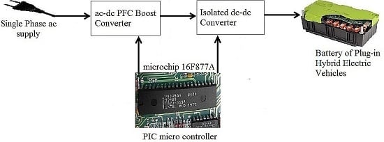
1. Introduction
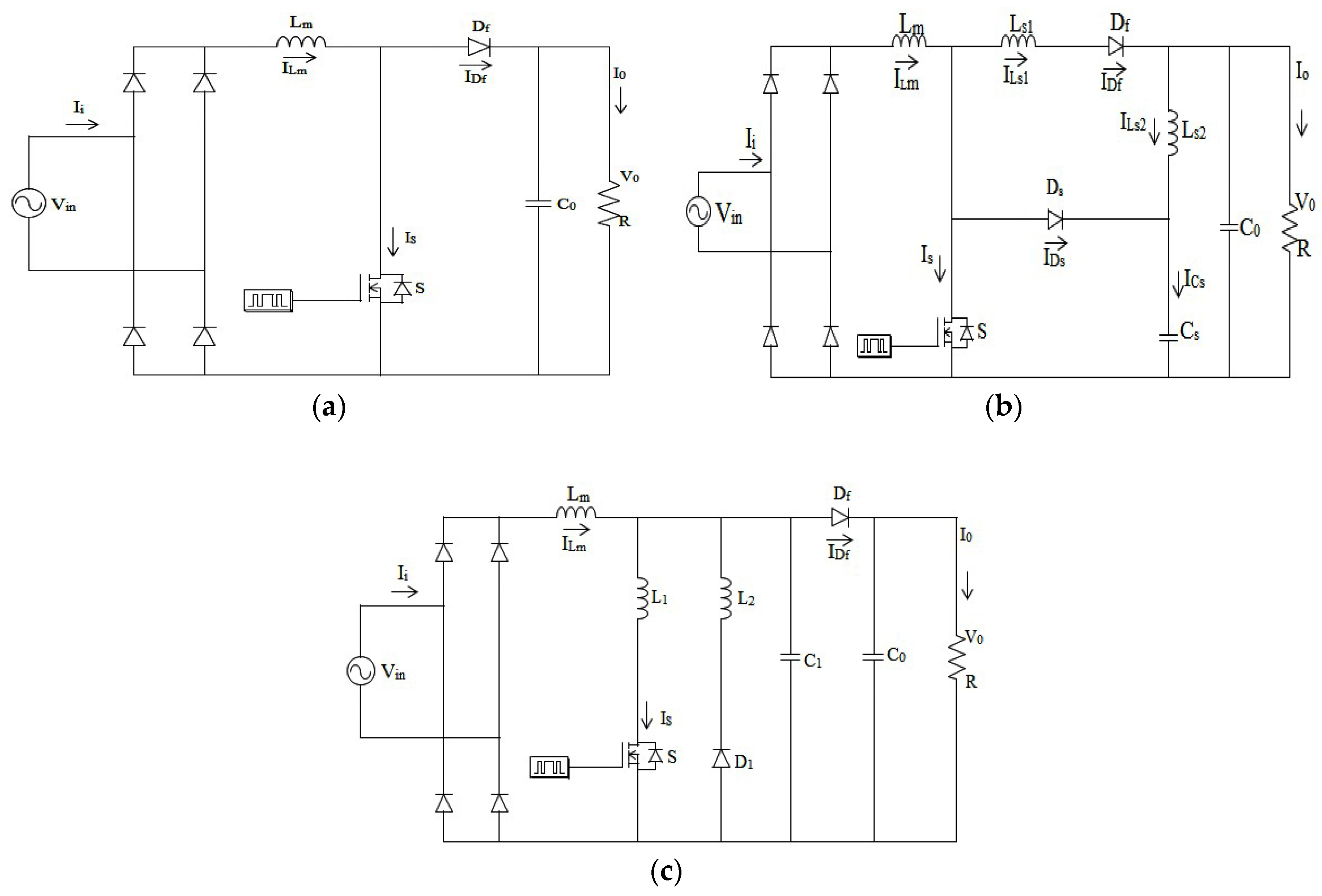
2. Review of Existing ac-dc PFC Boost Topologies

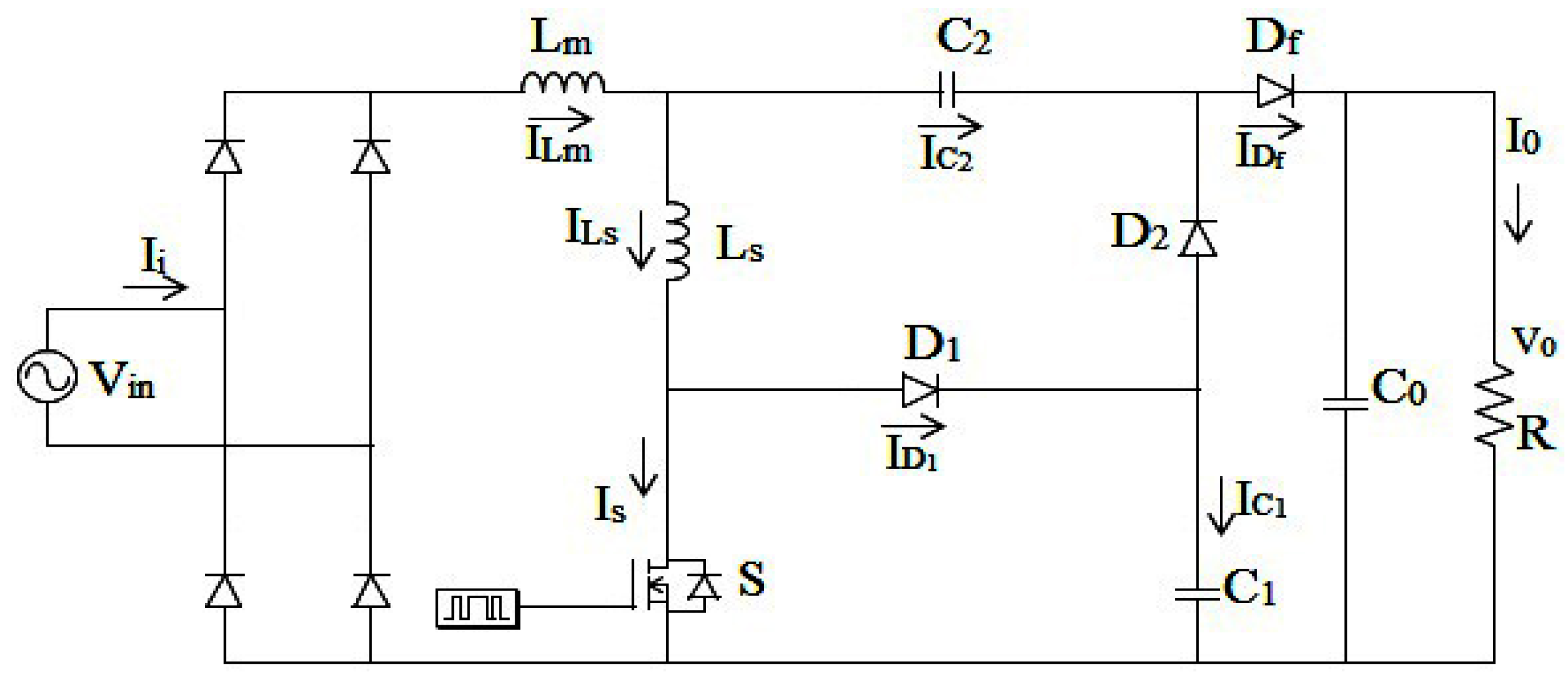
3. Circuit Structure of Proposed PFC Converter

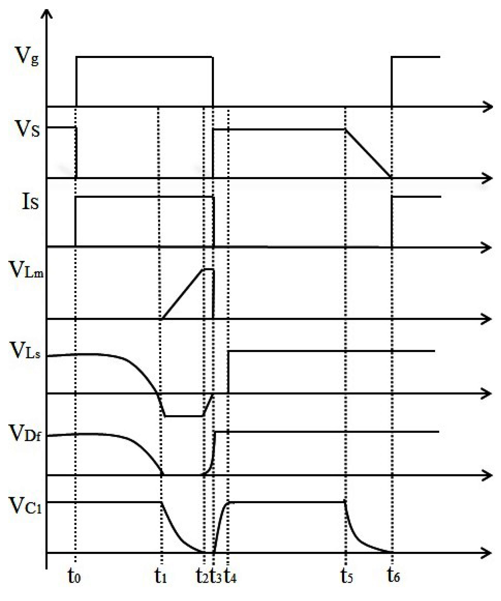
3.1. Operating Principle
- All the semiconductor devices used in the proposed converter are ideal.
- Reverse recovery of the boost converter diode is considered and taken into account.
- The output capacitor C0 is assumed to be large to produce a constant output voltage.
- The main inductor Lm is much greater than snubber inductor Ls to have a constant input current.


3.1.1. Mode 1 (t0 < t < t1)
3.1.2. Mode 2 (t1 < t < t2)
3.1.3. Mode 3 (t2 < t < t3)
3.1.4. Mode 4 (t3 < t < t4)
3.1.5. Mode 5 (t4 < t < t5)
3.1.6. Mode 6 (t5 < t < t6)
4. Design of Proposed LCD Snubber
4.1. Main Inductor Lm
4.2. Resonant Inductor LS
4.3. Resonant Capacitors C1 and C2
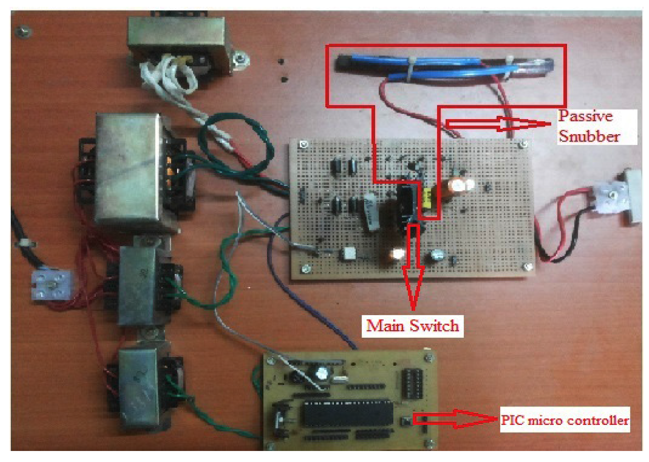
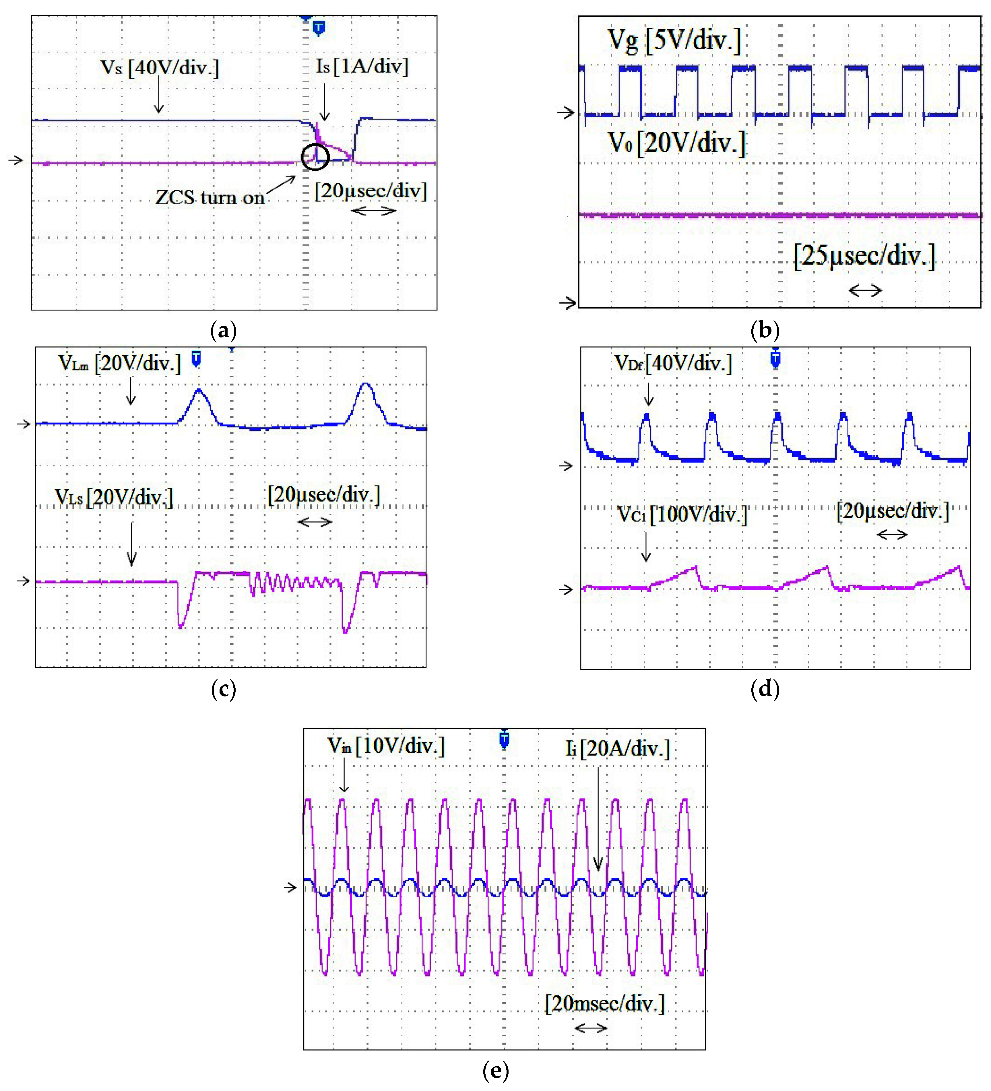
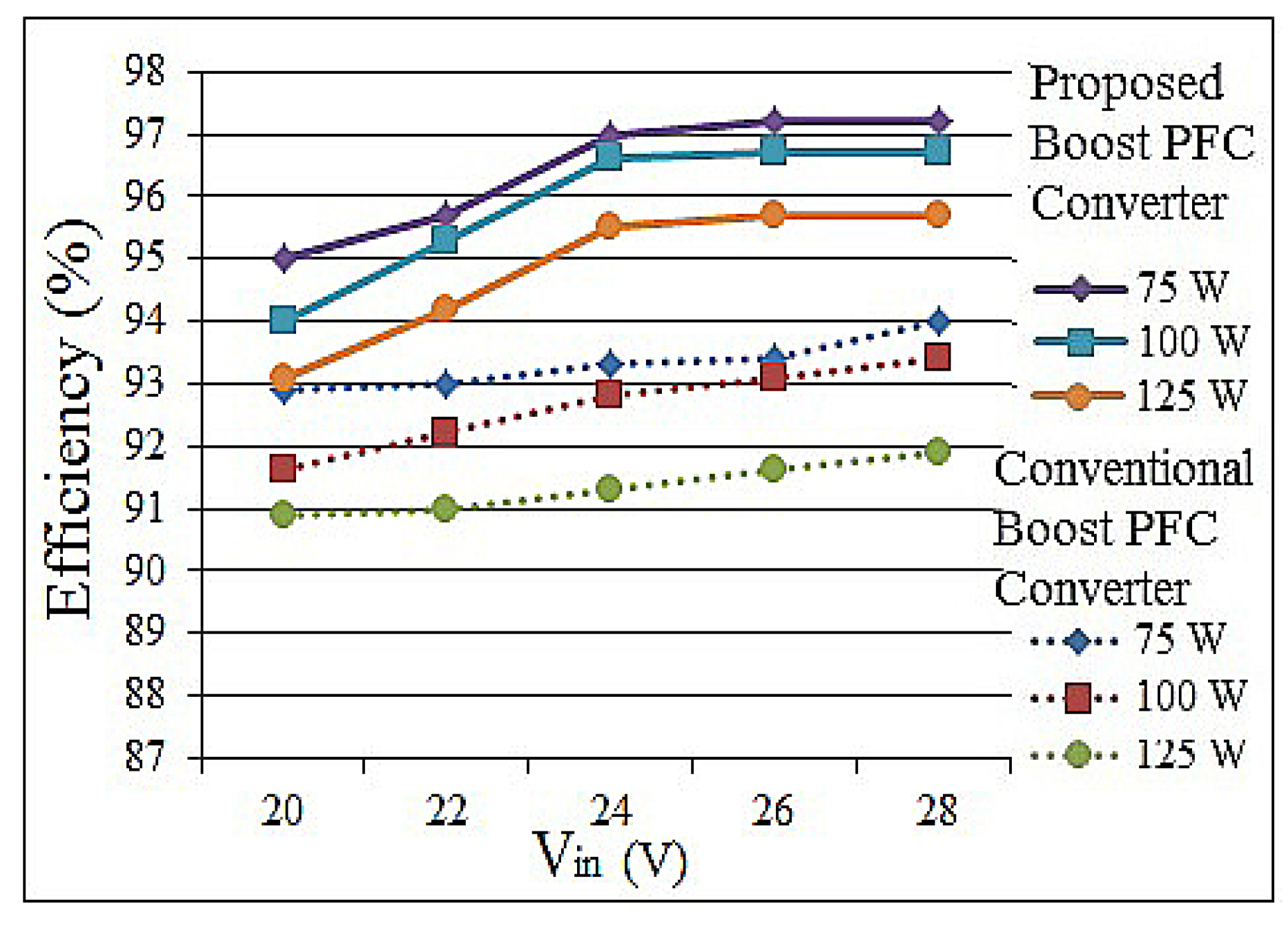
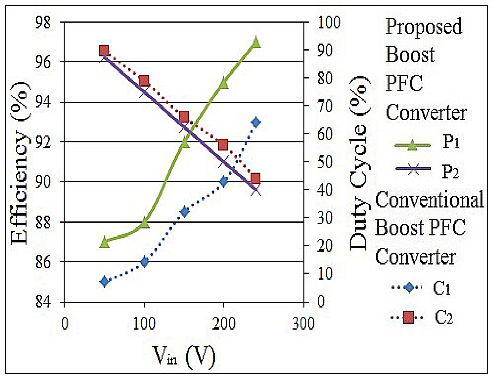
5. Experimental Results and Discussions


| Component | Company | ac-dc PFC Converter with Proposed Passive Snubber |
|---|---|---|
| Lm | JIME | 200 µH |
| C0 | nichicon | 90 µF |
| LS | - | 70 µH |
| C1 | Jb | 4.3 nF |
| C2 | nichicon | 2.5 µF |
| Rectifier Diode | MULTICOMP | 1N5408 (Vrrm = 1000V, If(max) = 1 A) |
| MOSFET | FAIRCHILD | IRF840 N-Channel Power MOSFETs, 8A, 450 V/500 V |
| High Frequency Diode | MIC | BA157 (Vrrm = 400V, Iavg = 1 A) |
| Transformer | JIME | Ferrite Core |
| Input Inductor | JIME | Ferrite Core |
| PIC Controller Chip | MICROCHIP | 16F877A |
| Optocoupler IsolationChip | Fairchild semiconductor | MCT2E |


| Circuit Type | Switching Features | Components Count | Power Factor | Efficiency (%) |
|---|---|---|---|---|
| Conventional Boost PFC | Hard Switching | No extra Component | 0.9641 | 91.18 |
| Boost PFC Passive snubber [33] | S—ZCS turn ON and ZVS turn OFF | 2 inductor | 0.98 | 95 |
| 1 Diode | ||||
| 1 capacitor | ||||
| Boost PFC Passive snubber [34] | S—ZCS turn ON and turn OFF | 2 inductor | 0.9897 | 95.3 |
| 2 Diode | ||||
| 1 capacitor | ||||
| Boost PFC Converter with proposed passive snubber | S—ZCS turn ON and ZVS turn OFF | 2 inductor | 0.9897 | 97 |
| 2 Diode | ||||
| 1 capacitor |
6. Conclusions
Conflicts of Interest
Nomenclature
| d | Switching duty cycle for the proposed converter. |
| D | Diode. |
| C | Capacitance (F). |
| t | Time (s). |
| tr | Rise time of the switch current (s). |
| tf | Fall time of the switch current (s). |
| Ton | On-time of the main switch (s). |
| R | Resistance of load resistor (Ω). |
| LS | Inductance of the snubber inductor of the passive circuit (H). |
| fs | Switching frequency (Hz). |
| S | Main switch. |
| Lm | Inductance of main inductor (H). |
| Df | Output diode of the boost converter. |
| C0 | Capacitance of output capacitor of the boost converter (F). |
| Cp | Parasitic capacitance of the switch (F). |
| Vin | Input ac voltage of the source (V). |
| Vdc | Input dc voltage of the boost converter (V). |
| V0 | Output dc voltage of the ac-dc boost PFC converter (V). |
| VC1 | Instantaneous voltage across the snubber capacitor C1 (V). |
| VC2 | Instantaneous voltage across the snubber capacitor C2 (V). |
| Vg | Gate to source voltage of the main switch S (V). |
| VLm | Instantaneous voltage across the main inductor Lm (V). |
| VLs | Instantaneous voltage across the snubber inductor Ls (V). |
| VDf | Instantaneous voltage of the output diode Df (V). |
| VS | Instantaneous voltage across the main switch S (V). |
| Ii | Input ac current of the single phase ac source (A). |
| I0 | Output dc current of the ac-dc boost PFC converter (A). |
| ILm | Instantaneous current of the main inductor Lm (A). |
| ILs | Instantaneous current of the snubber inductor Ls (A). |
| IDf | Instantaneous current of the output diode Df (A). |
| ID1 | Instantaneous current of the snubber diode D1 (A). |
| ID2 | Instantaneous current of the snubber diode D2 (A). |
| IS | Instantaneous current of the main switch S (A). |
| ∆IL | Current ripple of the main inductor Lm (A). |
| Po | Output power of the ac-dc boost PFC converter (W). |
| ωr | Resonant angular frequency (rad/sec). |
| List of Acronyms | |
| PFC | Power Factor Correction |
| ac | alternating current |
| dc | direct current |
| ac-dc | alternating current to direct current |
| ZCS | Zero Current Switching |
| ZVS | Zero Voltage Switching |
| ZC-ZVS | Zero Current- Zero Voltage Switching |
| MOSFET | Metal Oxide Semiconductor Field Effect Transistor |
| EMI | Electro Magnetic Interference |
| RCD | Circuit composed of a resistor R, a capacitor C and a diode D |
| PEV | Plug-in-Electric Vehicle |
| PHEV | Plug-in Hybrid Electric Vehicle |
| EV | Electric Vehicle |
| THD | Total Harmonic Distortion |
| RM | Ripple Mirror |
| CCM | Continuous Conduction Mode |
| LCD | Circuit composed of an inductor L, a capacitor C and a diode D |
| BEV | Battery Electric Vehicle |
References
- Morrow, K.; Karner, D.; Francfort, J. Plug-in Hybrid Electric Vehicle Charging Infrastructure Review; U.S. Department of Energy—Vehicle Technologies Program; INL/EXT-08-15058; Idaho National Laboratory: Idaho Falls, ID, USA, 2008. [Google Scholar]
- Shi, L.; Meintz, A.; Ferdowsi, M. Single-Phase Bidirectional ac-dc Converters for Plug-in Hybrid Electric Vehicle Applications. In Proceedings of the IEEE Vehicle Power and Propulsion Conference, Harbin, China, 3–5 September 2008; pp. 1–5.
- Musavi, F.; Eberle, W.; Dunford, W.G. A High-Performance Single-Phase Bridgeless Interleaved PFC Converter for Plug-in Hybrid Electric Vehicle Battery Chargers. IEEE Trans. Ind. Appl. 2011, 47, 1833–1843. [Google Scholar] [CrossRef]
- Tanoue, K.; Yanagihara, H.; Kusumi, H. Hybrid is a key technology for future automobiles. In Hydrogen Technology: Mobile and Portable Applications; Leon, A., Ed.; Springer Science & Business Media: Karlsruhe, Germany, 2008; pp. 235–272. [Google Scholar]
- Matthé, R.; Eberle, U. The voltec system: Energy storage and electric propulsion. In Lithium-Ion Batteries: Advances and Applications; Pistoia, G., Ed.; Elsevier Science: Oxford, UK, 2014; pp. 151–176. [Google Scholar]
- IEEE Recommended Practices and Requirements for Harmonic Control in Electric Power Systems; IEEE Std 519-1992; Institute of Electrical and Electronics Engineers: New York, NY, USA, 1992.
- IEEE Recommended Practice for Monitoring Electric Power Quality; IEEE Std 1159; Institute of Electrical and Electronics Engineers: New York, NY, USA, 1995.
- Huang, T.; Leu, Y.; Chang, Y.; Hou, S. An energy harvester using self-powered feed forward converter charging approach. Energy 2013, 55, 769–777. [Google Scholar] [CrossRef]
- Punitha, K.; Devaraj, D.; Sakthivel, S. Artificial neural network based modified incremental conductance algorithm for maximum power point tracking in photovoltaic system under partial shading conditions. Energy 2013, 62, 330–340. [Google Scholar] [CrossRef]
- Bouilouta, A.; Mellit, A.; Kalogirou, S.A. New MPPT method for stand-alone photovoltaic systems operating under partially shaded conditions. Energy 2013, 55, 1172–1185. [Google Scholar] [CrossRef]
- Tsai, C.T.; Shen, C.L. High efficiency current-doubler rectifier with low output current ripple and high step-down voltage ratio. IEEE Trans. Ind. Appl. 2013, 8, 182–189. [Google Scholar] [CrossRef]
- Erickson, R.W.; Maksimovic, D. Fundamentals of Power Electronics, 2nd ed.; Plenum Publishers: New York, NY, USA, 2001; pp. 1–791. [Google Scholar]
- Li, W.; He, X. Review of non-isolated high-step-up DC/DC converters in photovoltaic grid-connected applications. IEEE Trans. Power Electron. 2011, 58, 1239–1250. [Google Scholar]
- Gerard, M.; Poirot-Crouvezier, J.; Hissel, D.; Pera, M. Ripple current effects on PEMFC aging test by experimental and modeling. J. Fuel Cell Sci. Technol. 2010, 8. [Google Scholar] [CrossRef]
- Miwa, B.A.; Otten, D.M.; Schlecht, M.F. High efficiency power factor correction using interleaving technique. In Proceedings of the IEEE Applied Power Electronics Conference and Exposition, Boston, MA, USA, 23–27 February 1992; pp. 557–568.
- Huang, X.; Wang, X.; Nergaard, T.; Lai, J.S.; Xu, X.; Zhu, L. Parasitic ringing and design issues of digitally controlled high power interleaved boost converters. IEEE Trans. Power Electron. 2004, 19, 1341–1352. [Google Scholar] [CrossRef]
- Haroun, R.; Cid-Pastor, A.; El Aroudi, A.; Martinez-Salamero, L. Synthesis of canonical elements for power processing in DC distribution systems using cascaded converters and sliding-mode control. IEEE Trans. Power Electron. 2014, 29, 1366–1381. [Google Scholar] [CrossRef]
- Maksimovic, D.; Cuk, S. Switching converters with wide DC conversion range. IEEE Trans. Power Electron. 1991, 6, 151–157. [Google Scholar] [CrossRef]
- Lopez-Santos, O.; Martinez-Salamero, L.; Garcia, G.; Valderrama-Blavi, H.; Mercuri, D.O. Efficiency analysis of a sliding-mode controlled quadratic boost converter. IET Power Electron. 2013, 6, 364–373. [Google Scholar] [CrossRef]
- Al-Saffar, M.A.; Ismail, E.H.; Sabzali, A.J. Family of ZC-ZVS converters with wide voltage range for renewable energy systems. Renew. Energy 2013, 6, 32–43. [Google Scholar] [CrossRef]
- Ma, K.; Lee, Y.S. An integrated flyback converter for dc uninterruptible power supply. IEEE Trans. Power Electron. 1996, 11, 318–327. [Google Scholar] [CrossRef]
- Zhao, Q.; Lee, F.C. High-efficiency, high step-up DC-DC converters. IEEE Trans. Power Electron. 2003, 18, 65–73. [Google Scholar] [CrossRef]
- Wu, T.F.; Lai, Y.S.; Hung, J.C.; Chen, Y.M. Boost converter with coupled inductors and buck-boost type of active clamp. IEEE Trans. Ind. Electron. 2008, 55, 154–162. [Google Scholar] [CrossRef]
- Tseng, K.C.; Liang, T.J. Novel high-efficiency step-up converter. IEE Proc. Electr. Power Appl. 2004, 151, 182–190. [Google Scholar] [CrossRef]
- Wai, R.J.; Duan, R.Y. High-efficiency dc-dc converter with high voltage gain. IEE Proc. Electr. Power Appl. 2005, 152, 793–802. [Google Scholar] [CrossRef]
- Liang, T.J.; Chen, S.M.; Yang, L.S.; Chen, J.F.; Ioinovici, A. Ultra-large gain step-up switched-capacitor DC-DC converter with coupled inductor for alternative sources of Energy. IEEE Trans. Circuit Syst. I 2012, 59, 864–874. [Google Scholar] [CrossRef]
- Fardoun, A.A.; Ismail, E.H. Ultra step-up DC-DC converter with reduced switch stress. IEEE Trans. Ind. Appl. 2010, 46, 2025–2034. [Google Scholar] [CrossRef]
- Zhao, Y.; Li, W.; He, X. Single-phase improved active clamp coupled-inductor based converter with extended voltage doubler cell. IEEE Trans. Power Electron. 2012, 27, 2869–2878. [Google Scholar] [CrossRef]
- Aiswariya, S.; Dhanasekaran, R. Power Factor Correction Converter with an Active Snubber. In Proceedings of the International Conference on Modern Trends in Science Engineering and Technology, Dubai, UAE, 2–3 December 2013; pp. 71–74.
- Aiswariya, S.; Dhanasekaran, R. Simulation of a New Active Snubber for Power Factor Correction Converter Applications—A Performance Evaluation. Int. J. Appl. Eng. Res. 2015, 10, 5600–5605. [Google Scholar]
- Aiswariya, S.; Dhanasekaran, R. A New Soft Switched Boost PFC Converter With an Active Snubber. Int. J. Appl. Eng. Res. 2015, 10, 4325–4330. [Google Scholar]
- Aiswariya, S.; Dhanasekaran, R. An AC/DC PFC Converter with Active Soft Switching Technique. Int. J. Energy Optim. Eng. 2014, 3, 101–121. [Google Scholar] [CrossRef]
- Aiswariya, S.; Dhanasekaran, R. Simulation and Analysis of a Single Phase AC-DC Boost PFC Converter with a Passive Snubber for Power Quality Improvement. In Proceedings of the IEEE International Conference on Advances in Communication Control and Computing Technologies, Tamilnadu, India, 8–10 May 2014; pp. 421–425.
- Aiswariya, S.; Dhanasekaran, R. Efficiency Analysis of a New Passive Snubber for Battery Charging Applications. In Proceedings of the IEEE International Conference on Communication and Signal Processing, Melmaruvathur, Tamilnadu, India, 2–4 April 2015; pp. 17–22.
- Irving, B.; Jovanovic, M. Analysis, design, and performance evaluation of flying-capacitor passive lossless snubber applied to PFC boost converter. In Proceedings of the IEEE Applied Power Electronics Conference, Dallas, TX, USA, 10–14 March 2002; pp. 503–508.
- Mahesh, M.; Panda, A. A high performance single-phase AC-DC PFC boost converter with passive snubber circuit. In Proceedings of the IEEE Energy Conversion Congress and Exposition, Raleigh, NC, USA, 14–20 September 2012; pp. 2888–2894.
- Wu, H.; He, X. Single phase three-level power factor correction circuit with passive lossless snubber. IEEE Trans. Power Electron. 2002, 17, 946–953. [Google Scholar] [CrossRef]
- Jiang, S.-G.; Liu, G.-H.; Wang, W.; Xu, D.G. Research on bridgeless boost PFC with soft-switching. In Proceedings of the IEEE Vehicle Power and Propulsion Conference, Dearborn, MI, USA, 7–10 September 2009; pp. 1461–1464.
- Hwu, K.I.; Tsai, C.L.; Lin, K.F. A simple passive ZCS circuit for PFC converter. In Proceedings of the IEEE Applied Power Electronics Conference, Austin, TX USA, 24–28 February 2008; pp. 1022–1026.
- Schenk, K. Non Dissipative Snubber Circuit with Saturable Reactor. U.S. Patent 7, 233, 507, 19 June 2007. [Google Scholar]
- Joung, G.; Ma, K.; Kim, Y. Battery discharger applications of high frequency boost converter with lossless snubber. In Proceedings of the IEEE Power Electronics Specialists Conference, Cairns, Queensland Australia, 23–27 June 2002; pp. 938–942.
- Li, R.T.H.; Chung, H.S.-H.; Sung, A.K.T. Passive lossless snubber for boost PFC with minimum voltage and current stress. IEEE Trans. Power Electron. 2010, 25, 602–613. [Google Scholar] [CrossRef]
- Lai, C.-M.; Yang, M.-J.; Liang, S.-K. A Zero Input Current Ripple ZVS/ZCS Boost Converter with Boundary-Mode Control. Energies 2014, 7, 6765–6782. [Google Scholar] [CrossRef]
- Locment, F.; Sechilariu, M. Modeling and Simulation of DC Microgrids for Electric Vehicle Charging Stations. Energies 2015, 8, 4335–4356. [Google Scholar] [CrossRef]
- Wang, C.-S.; Li, W.; Meng, Z.; Wang, Y.-F.; Zhou, J.-G. Three-Phase High-Power and Zero-Current-Switching OBC for Plug-In Electric Vehicles. Energies 2015, 8, 6672–6704. [Google Scholar] [CrossRef]
- Tsai, C.-T.; Shen, C.-L.; Su, J.-C. A Power Supply System with ZVS and Current-Doubler Features for Hybrid Renewable Energy Conversion. Energies 2013, 6, 4859–4878. [Google Scholar] [CrossRef]
- Mültin, M.; Allerding, F.; Schmeck, H. Integration of Electric Vehicles in Smart Homes—An ICT-based Solution for V2G Scenarios. In Proceedings of the IEEE PES Innovative Smart Grid Technologies Conference, Washington, DC, USA, 16–18 January 2012; pp. 978–985.
© 2015 by the authors; licensee MDPI, Basel, Switzerland. This article is an open access article distributed under the terms and conditions of the Creative Commons by Attribution (CC-BY) license (http://creativecommons.org/licenses/by/4.0/).
Share and Cite
Sekar, A.; Raghavan, D. Implementation of Single Phase Soft Switched PFC Converter for Plug-in-Hybrid Electric Vehicles. Energies 2015, 8, 13096-13111. https://doi.org/10.3390/en81112359
Sekar A, Raghavan D. Implementation of Single Phase Soft Switched PFC Converter for Plug-in-Hybrid Electric Vehicles. Energies. 2015; 8(11):13096-13111. https://doi.org/10.3390/en81112359
Chicago/Turabian StyleSekar, Aiswariya, and Dhanasekaran Raghavan. 2015. "Implementation of Single Phase Soft Switched PFC Converter for Plug-in-Hybrid Electric Vehicles" Energies 8, no. 11: 13096-13111. https://doi.org/10.3390/en81112359