Article

High Efficiency Variable-Frequency Full-Bridge Converter with a Load Adaptive Control Method Based on the Loss Model

School of Electrical Engineering and Automation, Harbin Institute of Technology, Harbin 150001, China
*
Author to whom correspondence should be addressed.
These authors contributed equally to this work.
Energies 2015, 8(4), 2647-2673; https://doi.org/10.3390/en8042647
Submission received: 15 December 2014 / Revised: 3 March 2015 / Accepted: 6 March 2015 / Published: 1 April 2015
(This article belongs to the Collection Smart Grid)

Abstract

:
In this paper, a load adaptive control method to improve the efficiency and dynamic performance of the Phase-Shifted Full-Bridge (PSFB) converter which works under a wide range of load conditions is presented. The proposed control method can be used as a battery charger since this application demands a wide range of load conditions. The composition of the PSFB converter’s losses and the loss analysis model are both discussed. According to this model, the optimum switching frequency which results in minimum power loss is adopted to improve the efficiency. The relationship between switching frequency and power loss is formulated over a wide load range. Indicated by this kind of relationship, the proposed controller adjusts the switching frequency at different load currents. Moreover, an adaptive gain adjustment controller is applied to replace the traditional controller, with the aim to improve the dynamic performance which is influenced by the changes of the switching frequency and load current. In addition, the experimental results show that the maximum improvement of efficiency is up to 20%. These results confirm the effectiveness of the proposed load adaptive control method.

1. Introduction

To improve the efficiency of battery chargers, resonant converters are adopted to realize zero-voltage switching (ZVS). Considering its high efficiency and high power density, the phase-shifted full-bridge (PSFB) converter is applied in this paper. The PSFB converter provides ZVS for all primary switches, therefore the switching losses can be reduced significantly, and high efficiency and low Electro-Magnetic Interference (EMI) can also be achieved [1,2]. This converter has been widely employed in high power density applications, however, the converter operates under a wide range of load variations in battery charger applications [3,4]. The PSFB converter loses its ZVS capability under light-load conditions, then switching losses are increased significantly, and the efficiency becomes much lower [5].
Various methods to improve the efficiency of the PSFB converter have been investigated. With the help of an auxiliary coupled inductor, ZVS can be achieved over a much wider load range [6]. A wide range of ZVS can be obtained for the PSFB converter with clamp diodes and a resonant inductor, as proposed in [7]. All these proposed converters extend the ZVS range by adding an auxiliary circuit that provides enough energy to achieve complete ZVS for all switches. However the additional auxiliary circuit increases cost, complexity and causes extra losses.
Several methods have been proposed to improve the efficiency of the PSFB converter, especially under light load conditions, without any additional auxiliary circuits. By adjusting the switching control technique of the full-bridge converter [8], the efficiency improvement can be up to 20% under light loads. However, the switches are operated with hard switching transitions which results in serious EMI. Moreover, the control method requires complex control signals. The methods shown in [9,10] can reduce the switching losses by widening the dead-time to improve the efficiency under light load conditions. These methods are very effective only when the converter operates in the discontinuous conduction mode (DCM).
In order to improve the efficiency, it is necessary to understand the efficiency model. The efficiency of PSFB converter is a function of many variables such as switching frequency, load current and input/output voltage. The design optimization requires the optimum selection of all these parameters to achieve maximum efficiency. However, the design involves many parameters from different engineering fields (electrical, thermal, and magnetic), making it difficult to select them. To simplify the efficiency-based optimization procedure, designers usually select these parameters under a given set of pre-defined operating conditions [11].
The switching frequency is a key parameter to be optimized for the converter. However, an optimized switching frequency may achieve its maximum efficiency only under the given set of operating conditions, whilst under different operating conditions there is actually a degradation of the conversion efficiency [12]. Such designs would not be suited to a wide range of load conditions. The variable switching frequency control method has been adopted in the wide load range dc-dc converters to improve the efficiency. In [11,12], the switching frequency varies nonlinearly while tracking the converter maximum efficiency point under variable operation conditions. In [13,14], a buck converter with variable frequency operation according to the load current is proposed. The converter operating with lower switching frequency results in higher efficiency at light loads. In all of these cases, the buck converter is researched to verify the developed algorithm operation. These techniques have wide variations in switching frequency, which make it difficult to design filter and control circuits, so these techniques are hard to employ in the PSFB converter, because of the existence of transformer, filter inductance, leakage inductance and complex control circuits.
In this paper, a load adaptive control method to improve the efficiency of the PSFB converter which works under a wide range of load conditions is presented. The controller adjusts the switching frequency according to the relationship between the optimum switching frequency and load current. Moreover, in order to improve the dynamic performance, which is influenced by the changes of switching frequency and load current, an adaptive gain adjustment controller is applied to replace the traditional controller.
This paper is organized as follows: In Section 2 the loss analysis model of a PSFB converter operating in the continuous conduction mode (CCM) and discontinuous conduction mode (DCM) is presented. Section 3 discusses the loss distributions and the effect of switching frequency on the loss. The loss model is verified by experimental results. The proposed control system is described in Section 4. In Section 5, the experimental results are presented and discussed. The conclusion is given in Section 6.

2. Loss Analysis Model of the PSFB Converter

A sufficiently detailed loss analysis model is necessary in order to perform efficiency optimization. The power loss analysis is discussed in this section to help understand where the losses originate. There are three types of power loss for a switching power converter [15], as follows:
(1)
Switching power losses (including gate-drive power losses). Voltage and current cross over during switching transitions, which results in switching power losses. These losses are related to the switching frequency, the voltage across the switches, and current through the switches. The gate of the device being charged causes the gate-drive power loss. It is related to the gate charge value, the switching frequency, and the gate-drive voltage.
(2)
Conduction power losses. These losses are mainly caused by the parasitic resistance in the components, such as the on resistance of the transistor, the transformer and inductor winding resistance. They can be calculated from the equivalent resistance and the rms current value in different branches in the converter.
(3)
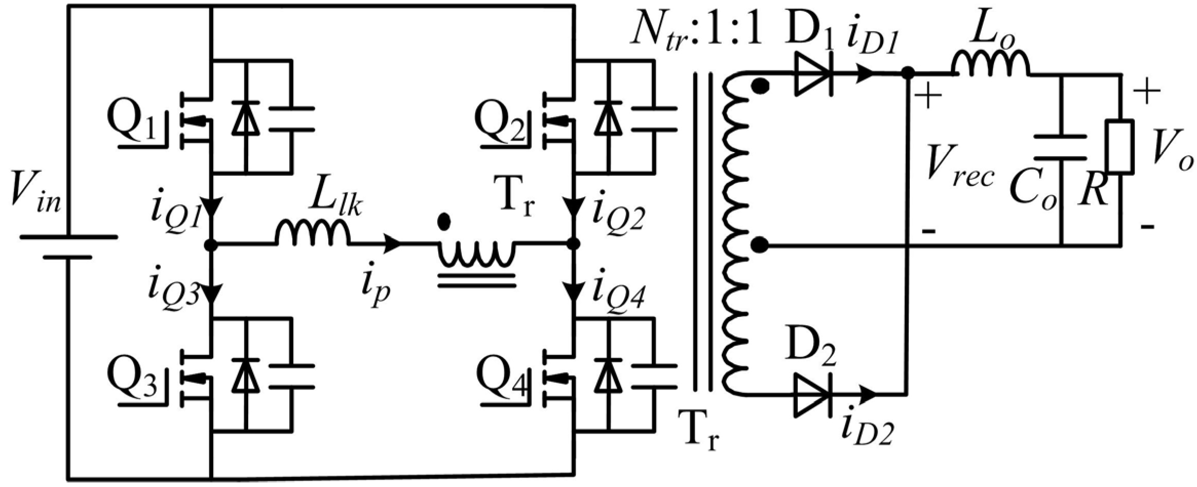
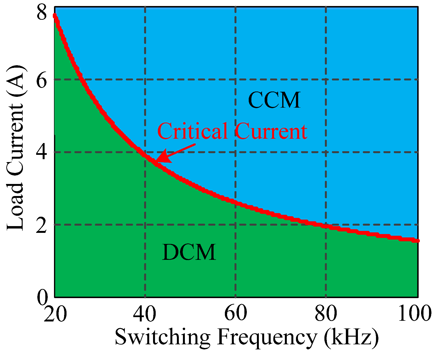
Magnetic core power losses. The total magnetic core losses are the sum of hysteresis loss, residual loss and eddy current loss. The empirical methods based on measurement observations are one major group of core losses calculations. A widely used empirical-method is the Steinmetz equation [16]:
P C O R E = k f s α B β V e
where fs is the frequency in Hz; B is the peak flux density in Tesla; Ve is the effective volume of the core in m3; and k, α, β are constant which can be obtained from the core material datasheet. This equation has proven to be an effective method for the calculation of the magnetic core power losses. The circuit diagram of the PSFB converter is shown in Figure 1. The PSFB converter’s operation can be classified into DCM and CCM according to whether there is always current through the output filter inductor or not. The circuit analysis in CCM is quite different from that in DCM because of its different equivalent circuit.
Figure 1. Circuit diagram of a PSFB converter.
Energies 08 02647 g001

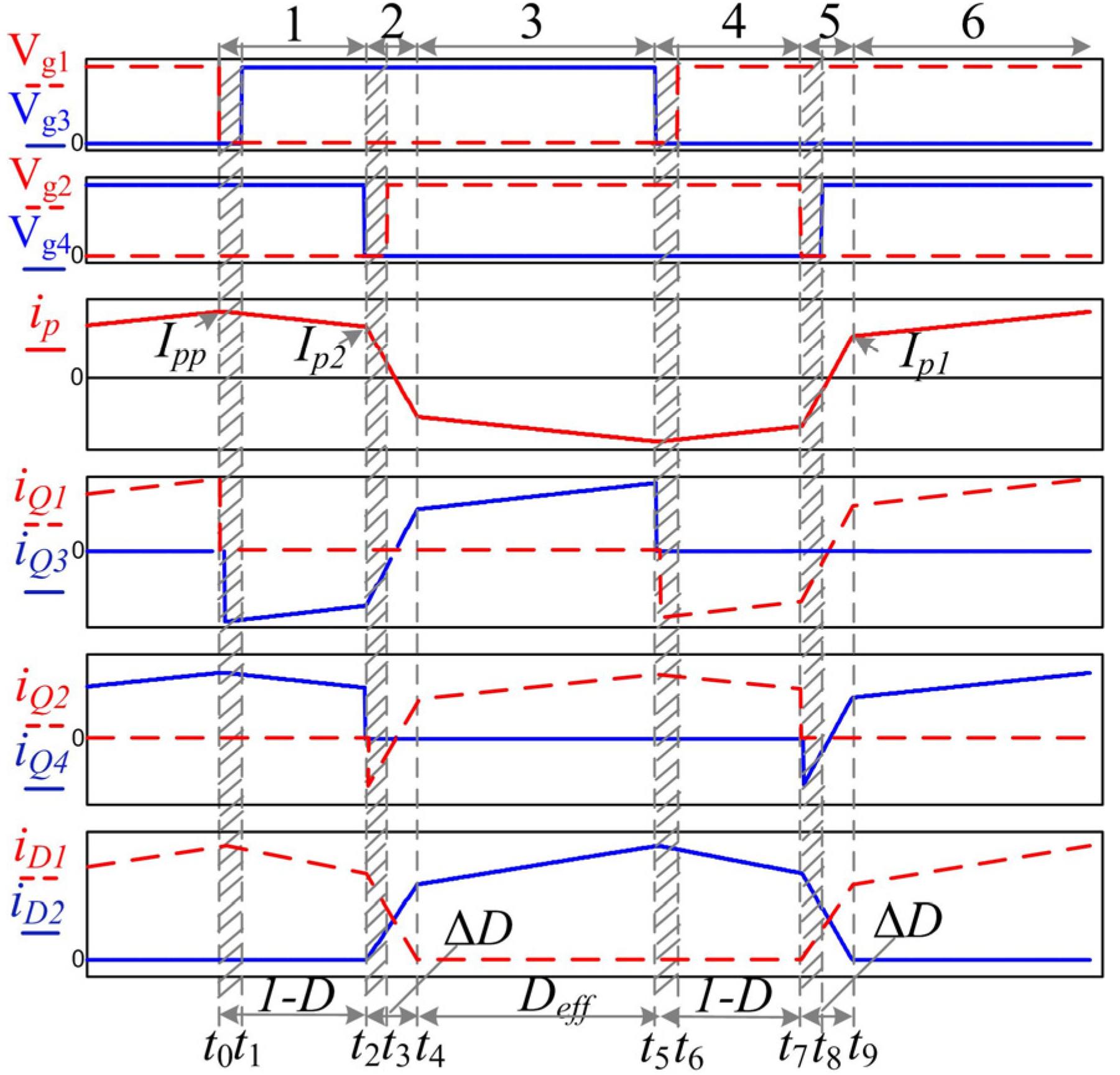
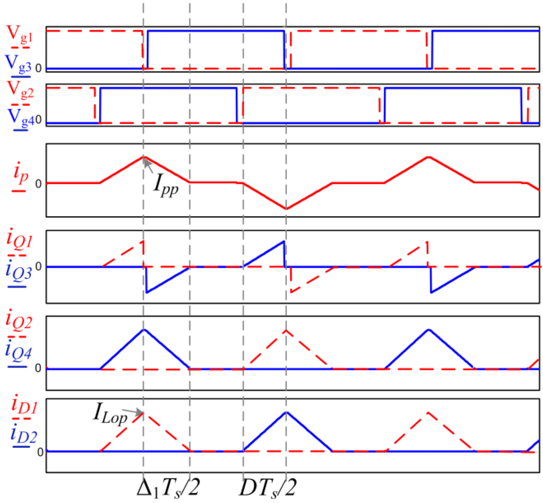
2.1. The Circuit Analysis in CCM Operation

Figure 2 shows the key waveforms in CCM operation. The converter is controlled by the phase-shift method. For the convenience of circuit analysis, the following assumptions are made: (1) all components have ideal characteristics and properties; (2) all parameters of the same kind of devices have the same values; (3) Ntr2Lo is much larger than the value of Llk.
Figure 2. Key waveforms of the PSFB converter in CCM operation.
Energies 08 02647 g002
The voltage gain of the PSFB converter is:
V o V i n = D e f f N t r
where Deff is the effective duty cycle of the secondary voltage.
The duty cycle of the primary voltage which is set by the controller, can be expressed as:
D = D e f f + Δ D
where ΔD is the loss of duty cycle. ΔD is caused by the finite slope of the rising and falling edges of the primary current due to the presence of the resonant inductor Llk [17]. During the interval of ΔD, the primary current changes from Ip2 to −Ip1 and ΔD is calculated as:
Δ D = 2 L l k f s ( I p 1 + I p 2 ) V i n
The current ripple of the output filter inductor is:
Δ I o u t = 0.5 V i n / N   t r V o u t L o D e f f 2 f s
The peak value of the primary current Ipp that corresponds to the output filter inductor current reflected to the primary side is described as:
I p p = I o + Δ I o u t N t r
The primary current at t9 and t2 can be derived from the steady-state analysis:
I p 1 = I o Δ I o u t N t r
I p 2 = I p p V o 1 D 2 f s N t r L o
As shown in Figure 2, the operation of the PSFB converter is divided into six intervals if the dead-time is ignored, which is marked by an oblique line. Since intervals 1–3 and 4–6 are symmetrical, only intervals 1–3 will be discussed [17,18].
(1) Interval 1 [t0~t2]: The primary current increases to Ipp at t0. Q1 is turned off at the same time. The capacitances of Q1 and Q3 charge and discharge, respectively. During this interval, the output filter inductor reflects to the primary side. Q3 can achieve ZVS easily. After Q3 is turned on at t1, the primary current circulates through Q3 and Q4. When the dead time between Q1 and Q3 is ignored, the primary current decreases from Ipp to Ip2. The primary current is:
i p 02 ( t ) = I p p + I p 2 I p p ( 1 D ) T s / 2 ( t t 0 )
The value of current through D1 can be calculated as:
i D 102 ( t ) = N t r i p 02 ( t )
(2) Interval 2 [t2~t4]: At the beginning of this interval, Q4 is turned off, and resonance occurs between the output capacitances of Q2, Q4 and the resonant inductor Llk. During this interval, the secondary winding voltages of the transformer are zero since the diodes D1 and D2 conduct at the same time. This interval is known as the duty cycle loss and it decreases the effective duty cycle of the secondary side. No energy is transferred to the output side. D1 current decreases while D2 current increases. The sum current of D1 and D2 is equal to the load current. The primary current decreases from Ip2 to −Ip1 and is calculated as:
i p 24 ( t ) = I p 2 I p 1 + I p 2 Δ D T s / 2 ( t t 2 )
The values of current though D1 and D2 are calculated as follows, respectively:
i D 124 ( t ) = N t r [ I p 2 I p 2 Δ D T s / 2 ( t t 2 ) ]
i D 224 ( t ) = N t r I   p 1 Δ D T s / 2 ( t t 2 )
(3) Interval 3 [t4~t5]: In this interval, the energy is transferred to the output side and this interval is called effective duty. The primary current increases from Ip1 to the peak value Ipp and is calculated as:
i p 45 ( t ) = I p 1 + I p p I p 1 D e f f T s / 2 ( t t 4 )
The current of D2 can be expressed as:
i D 245 ( t ) = N t r i p 45 ( t )

2.2. The Loss Analysis in CCM Operation

There are three types of power loss for a switching power converter: conduction losses, switching losses, and magnetic core losses. Generally speaking, conduction losses are related to the load current, switching losses depend on the switching frequency and magnetic core losses are determined by the core material. Based on the key waveforms of the PSFB converter in Figure 2, the total power loss can be calculated as follows:

2.2.1. Total Conduction Losses

The conduction losses can be calculated from the parasitic resistances of the components and the rms current values in different branches in the converter. The rms primary current’s squared value is:
I 2 p , r m s = 2 T s t 0 t 5 i 2 p ( t ) d t = ( 1 D ) I p 2 2 + I p p 2 + I p 2 I p p 3 + Δ D I p 2 2 + I p 1 2 I p 2 I p 1 3 + D e f f I p 1 2 + I p p 2 + I p 1 I p p 3
Since the PSFB converter is controlled with the phase-shift method, the duty cycle of each primary switch driver signal is 50% (as shown in Figure 2) if the dead time is ignored. The conduction time of each primary switch is half of the switching cycle and the rms current through the MOSFET is:
I M O S , r m s = I p , r m s 2
The rms current’s squared value through the rectifier diode is calculated as:
I 2 D i o , r m s N 2 t r = 1 T s N 2 t r t 2 t 7 i 2 D 2 ( t ) d t = D e f f ( I p 1 2 + I p p 2 + I p 1 I p p ) 6 + Δ D I p 1 2 + I p 2 2 6 + ( 1 D ) I p 2 2 + I p p 2 + I p 2 I p p 6
The average current through the rectifier diode is:
I D i o , a v e = 1 T s t 2 t 7 i D 2 ( t ) d t = N t r 4 ( 1 D ) ( I p 2 + I p p ) + Δ D ( I p 1 + I p 2 ) + D e f f ( I p 1 + I p p )
The rms current of the output filter inductor Lo is:
I I n d , r m s = I 2 o + Δ I 2 o u t 3
The conduction loss of the MOSFET is expressed as:
P c Q = R Q o n I 2 M O S , r m s
where RQon is the on-state resistance of the MOSFET that can be obtained from its datasheet.
The conduction loss of the transformer is:
P c T R = R T R p r i I 2 p , r m s + 2 R T R sec I 2 D i o , r m s
where RTrpri is the resistance of the primary winding of the transformer and RTrsec is the resistance of the secondary winding. The maximum switching frequency is selected as 100 kHz in order to reduce the influence of limit cycle in the digital control system [19]. The penetration depth of copper conductor is 0.25 mm at 100 kHz, 100 °C [20]. The specification of the primary side Litz wire is 0.2 × 30, where the wire diameter d is 0.2 mm (smaller than the penetration depth) and the number of strands is 30. The influence of skin effect can be ignored.
The conduction loss of filter inductor is calculated as:
P c I N D = R I N D I 2 I n d , r m s
where RIND is the inductor dc resistance.
The conduction loss of rectifier diode is decided by the forward voltage drop VF and the average current through the diode. It can be calculated as:
P c D = V F I D i o , a v e
Therefore, the total conduction losses can be described as:
P c T o t a l = 4 P c Q + P c T R + P c I N D + 2 P c D
Figure 3 shows the switching frequency effect on the total conduction losses at output current Io = 10 A according to Equation (25). As shown in Figure 3, higher switching frequency results in lower conduction losses. This is because that higher switching frequency results in lower ripple and less rms current.
Figure 3. Switching frequency effect on the conduction losses at Io = 10 A.
Energies 08 02647 g003

2.2.2. Total Switching Losses

The overlap of voltage and current during switching transition results in switching power losses. Switching losses constitute a significant portion of the total losses. These losses can be calculated based upon the switch voltage and current waveforms during switching transitions [15,21]. The switching losses of a MOSFET include turn-off loss and turn-on loss. The PSFB converter provides ZVS-on for the switches. Turn-on loss is approximately zero under CCM operation condition. However, the device may lose its ZVS-on capability under DCM operation condition.
According to the waveforms of the converter in Figure 2, the turn-off loss of leading-leg Q1 or Q3 can be estimated by the following equation:
P Q 13 O F F = 0.5 V i n I p p ( t d O F F + t f ) f s
The turn-off loss of lagging-leg Q2 or Q4 is:
P Q 24 O F F = 0.5 V i n I p 2 ( t d O F F + t f ) f s
where tdOFF is the turn-off delay of the MOSFET; tf is the falling time of the MOSFET switching control. These parameters can be found in the datasheet.
The gate-drive power loss is due to the input capacitance of the MOSFET when charged/discharged. It is decided by the gate-drive voltage, the switching frequency and the gate charge value. It can be expressed as:
P Q d r = Q g V d r f s
where Qg is the gate charge value; Vdr is the gate-drive voltage.
From the equations shown before, the total switching losses caused by a MOSFET can be calculated as:
P Q = 2 P Q 13 O F F + 2 P Q 24 O F F + 4 P Q d r
The switching losses of rectifier diodes are difficult to calculate. The method proposed in [22] makes it possible to do the calculation using the datasheet values. The turn-on loss can be expressed as:
P d O N = 0.5 N t r I p 1 V F R t f r f s
where VFR is the forward recovery voltage; and tfr is the turn-on recovery time.
The turn-off loss of rectifier diodes can be calculated as:
P d O F F = 0.5 N t r I p 2 V R f s t r r / 2
where VR is the reverse voltage; trr is the reverse recovery time.
Therefore, the total switching losses is:
P S W T o t a l = P Q + 2 ( P d O F F + P d O N )
Figure 4 shows the switching frequency effect on the total switching losses at Io = 10 A according to Equation (32). It shows that higher switching frequency results in higher switching losses.
Figure 4. Switching losses versus switching frequency.
Energies 08 02647 g004

2.2.3. Magnetic Core Losses

The core losses can be calculated using the Steinmetz Equation (1). This equation has proven to be an effective method for the calculation of the magnetic core power losses.
The magnetic flux density of the transformer is:
B T r = V i n D 4 f s A e T r N p
where Ae-Tr is the cross-sectional area of the transformer; Np is the turns of primary winding.
The ac peak flux density of the output filter inductor is:
B L o = μ r μ 0 N L o Δ I o 2 l e
where le is the magnetic path length; NLo is the turns of the inductor.
The core loss of transformer PcoreTR, and filter inductor PcoreLo, can be calculated as Equation (1). The magnetic core material is PC40 and α, β, k are 1.46, 2.57 and 2, respectively [23]. The total losses of magnetic core can be expressed as:
P c o r e T o t a l = P c o r e T R + P c o r e L o
Based on Equation (35), Figure 5 shows plots of the losses of magnetic components versus switching frequency. Higher switching frequency results in lower flux density according to Equations (33) and (34). According to the core loss model, the flux density has a greater influence on the core loss than switching frequency. PcoreTR and PcoreLo decrease while switching frequency increases, respectively.
Magnetic core loss dissipates in the form of heat and results in a temperature rise. Williams’ thermal model can be used to evaluate the temperature rise of the core [21]. The temperature rise is a function of magnetic core loss. In order to validate the core loss model, Figure 6 shows the experimental temperatures of the transformer and the output filter inductor with different switching frequencies under heavy load. It shows that temperature rise decreases while switching frequency increases. The results conform with the core loss model.
Figure 5. Core losses versus switching frequency.
Energies 08 02647 g005
Figure 6. Temperatures of magnetic components with different switching frequencies (a) Temperature of transformer; (b) Temperature of filter inductor.
Energies 08 02647 g006
The total losses can be described as:
P T o t a l = P c o n d T o t a l + P S W T o t a l + P c o r e T o t a l
The efficiency of the PSFB converter can be stated as:
η = V o I o V o I o + P T o t a l

2.3. The Loss Analysis in DCM Operation

If the load current is smaller than the current ripple of Lo, ΔIout, the current through Lo is discontinuous and the converter operates in DCM. The critical load current between CCM and DCM can be obtained based on Equation (5). Figure 7 shows switching frequency effect on the critical load current. As shown in Figure 7, the critical current decrease while switching frequency increases since higher frequency results in lower current ripple.
Figure 7. Switching frequency effect on the critical current.
Energies 08 02647 g007
The operation principle of the PSFB converter in DCM operation is different from that in CCM operation. Figure 8 shows the key waveforms of the PSFB converter in DCM operation.
Figure 8. Key waveforms of the PSFB converter in DCM operation.
Energies 08 02647 g008
The duty cycle D, is a function of the load current Io:
D = 4 L o I o f s V o N t r 2 V i n ( V i n V o N t r )
Δ 1 = D + D 2 + 16 L o I o f s / V o 2
The peak value of output filter inductor can be expressed as:
I L o p = ( V i n / N t r V o ) D 2 L o f s
The peak value of the primary current Ipp that corresponds to ILop reflected to the primary can be expressed as:
I p p = I L o p N t r
The conduction loss and magnetic core loss in DCM operation can be established in the same way as in CCM operation. However the switching loss in DCM operation is quite different from that in CCM operation. The leading-leg switches can still achieve ZVS-on. The lagging-leg switches and rectifier diodes are turned on and turned off with zero current switching in DCM operation, as shown in Figure 8. The switching losses are mainly caused by discharging/charging the output capacitance of switches and the junction capacitance of diodes. The switching losses of PSFB converter in DCM operation can be calculated as follows:
P S W = 4 * 1 / 2 C o s s V i n 2 f s + 2 C d i o ( V o 2 + V s e c 2 ) f s
where Coss is the output capacitance of primary switch; Cdio is the junction capacitance of rectifier diode.

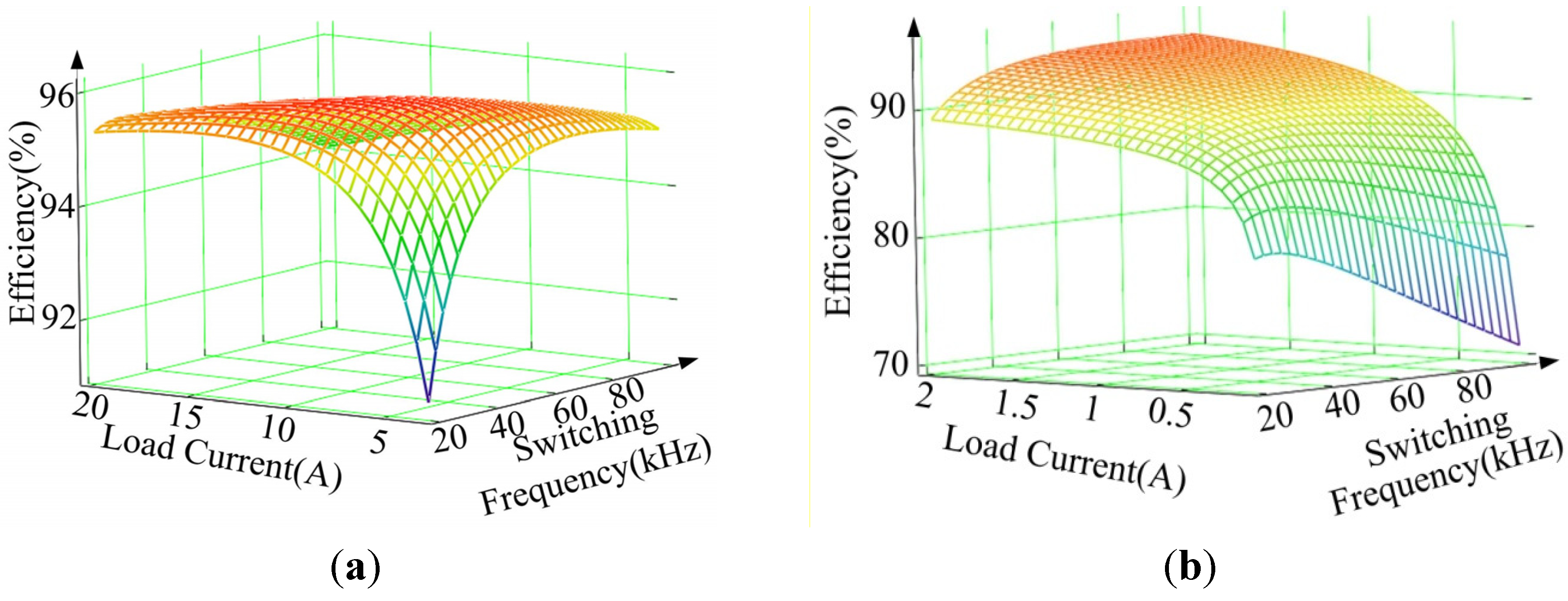
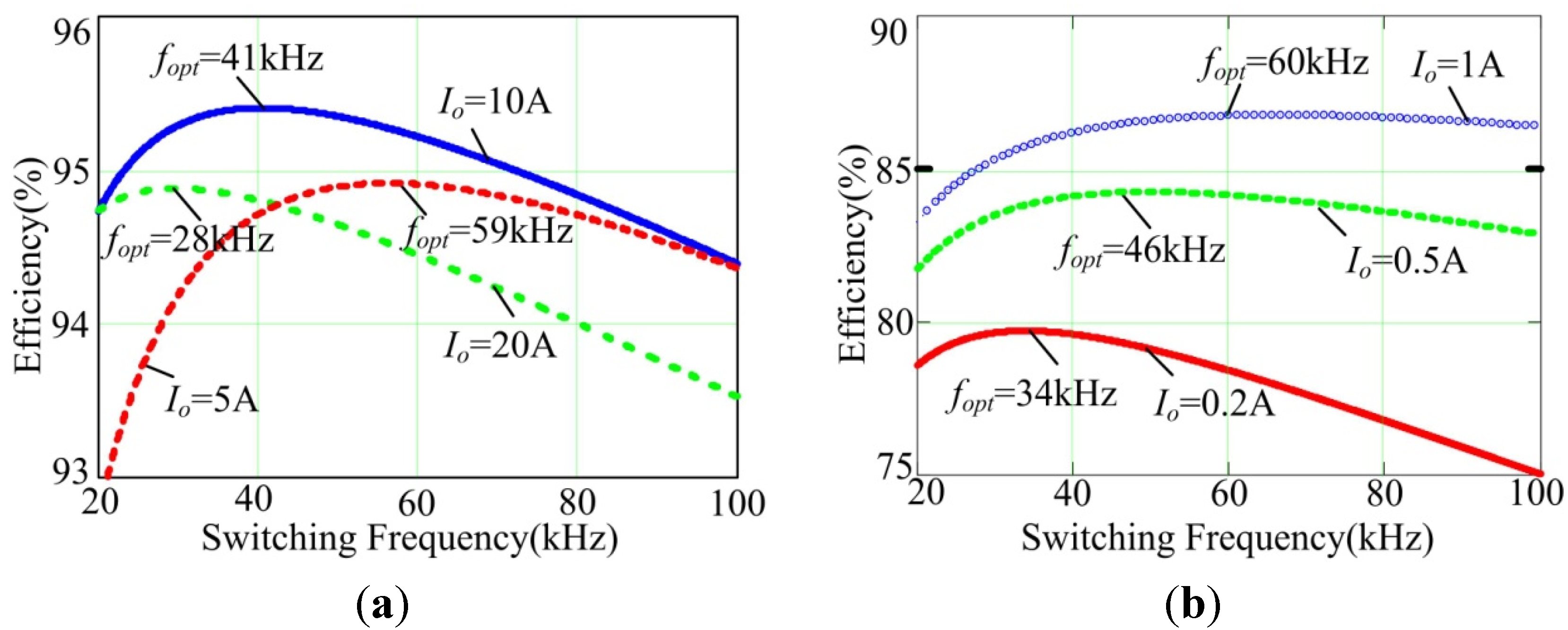
3. Switching Frequency Effect on Efficiency

Based on the analysis above, the power loss is a function of the switching frequency. The switching losses increase with the frequency while the magnetic core losses and conduction losses decrease since higher switching frequency leads to lower flux swing and less ripple current and rms current. The minimum total power loss means the maximum efficiency.

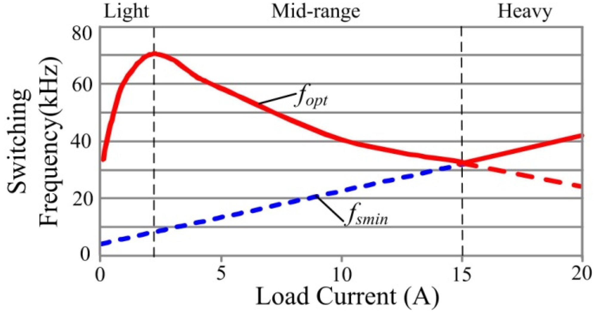
3.1. Optimum Switching Frequency

Based on Equation (37), Figure 9 shows 3-D surface plots of efficiency versus frequency versus load current in CCM operation and DCM operation. As shown in Figure 9, there is an optimum switching frequency which results in maximum efficiency for any specific load current. However, the optimum switching frequency varies with the load current.
Figure 9. 3-D plots of efficiency versus frequency versus load current; (a) CCM; (b) DCM.
Energies 08 02647 g009
For simpler visualization, one can observe Figure 10 which shows efficiency versus frequency at different load currents. These curves show clearly that the optimum switching frequency varies with the load current.
Figure 10. Efficiency versus frequency at different load currents (a) CCM; (b) DCM.
Energies 08 02647 g010

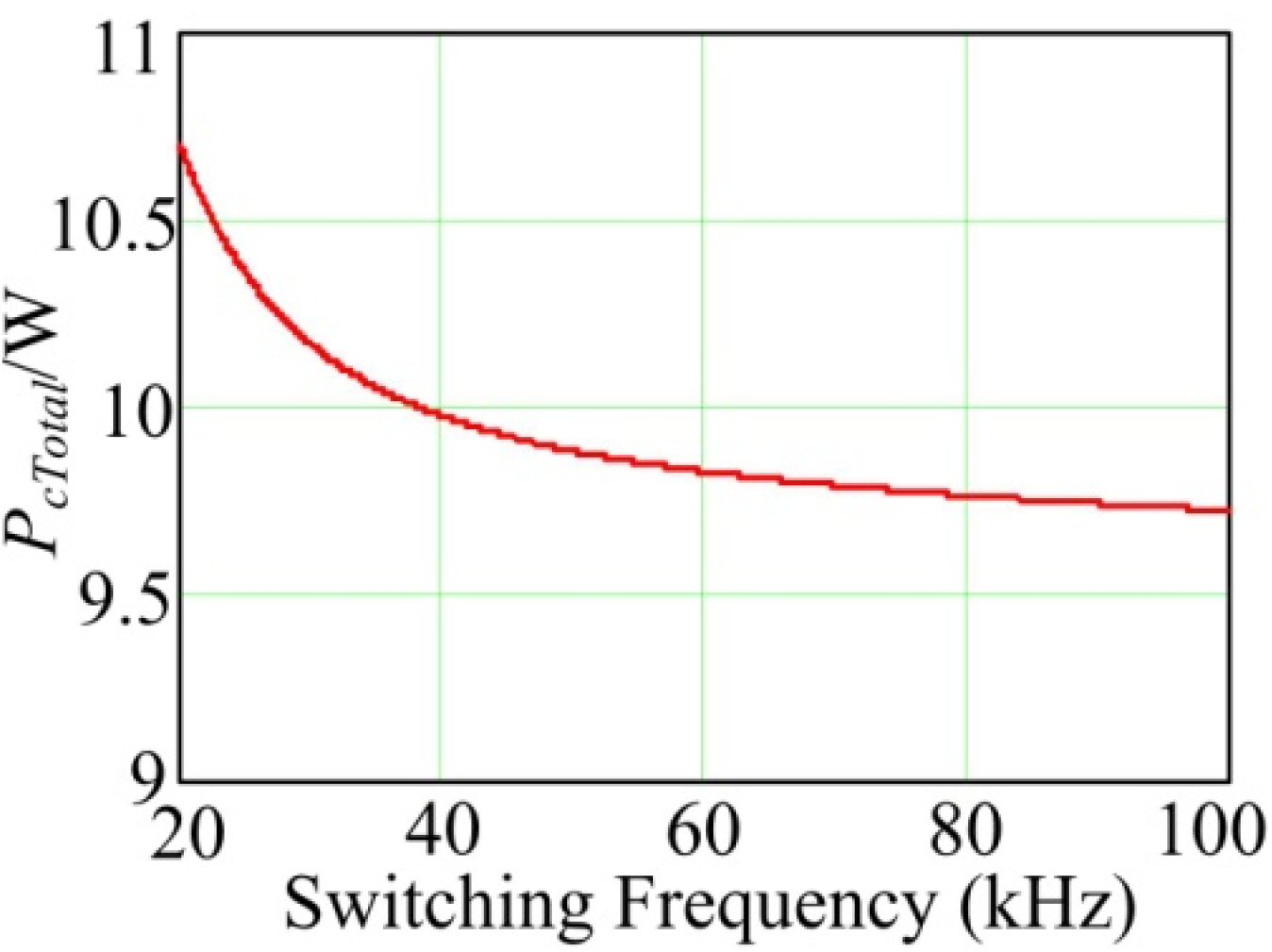
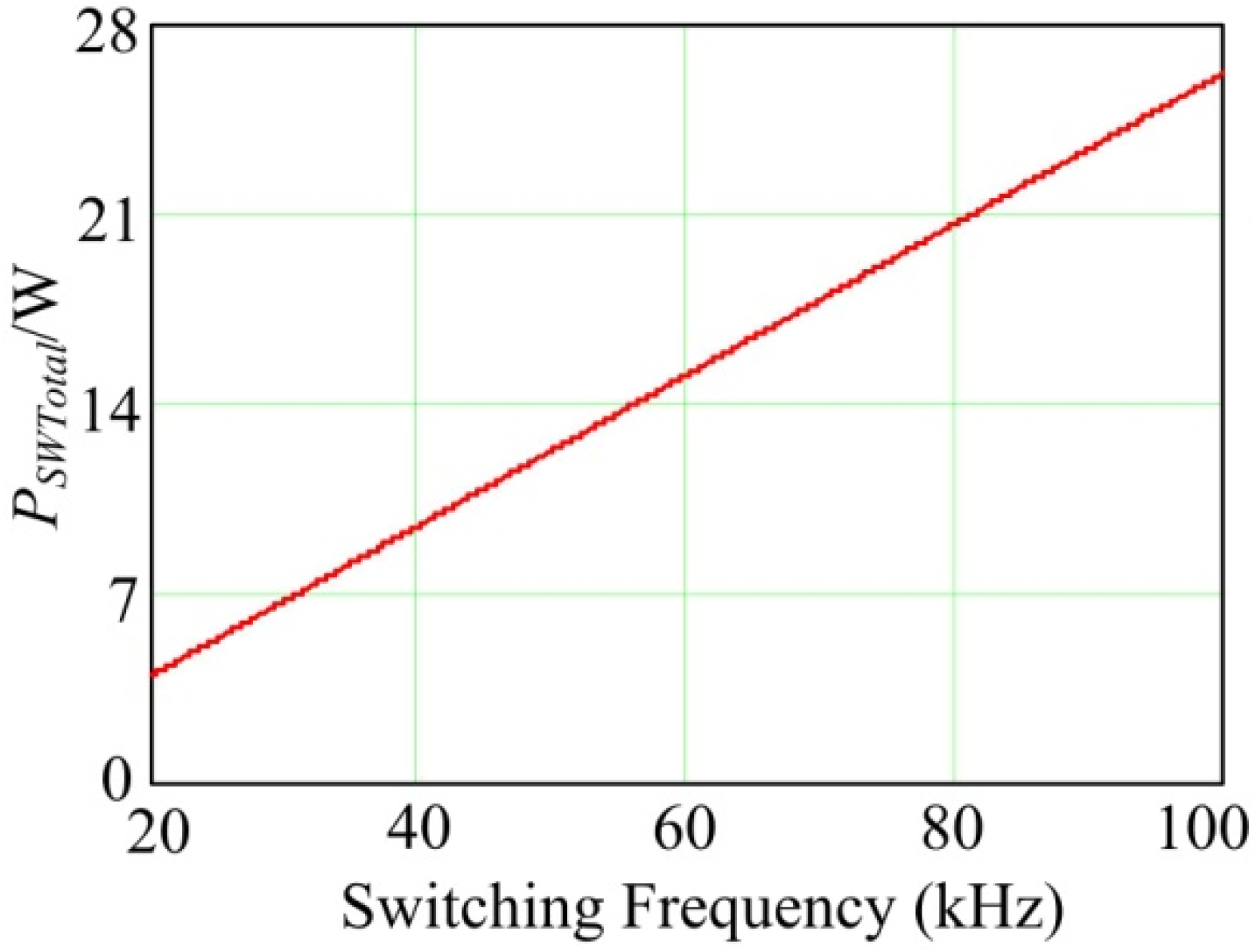
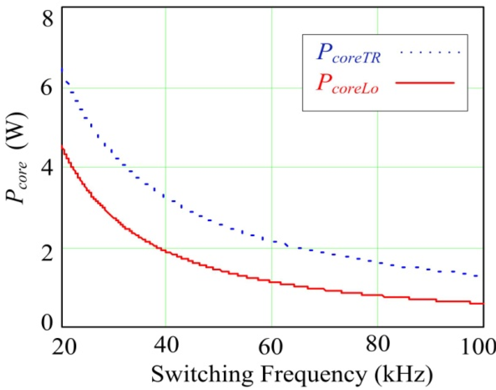
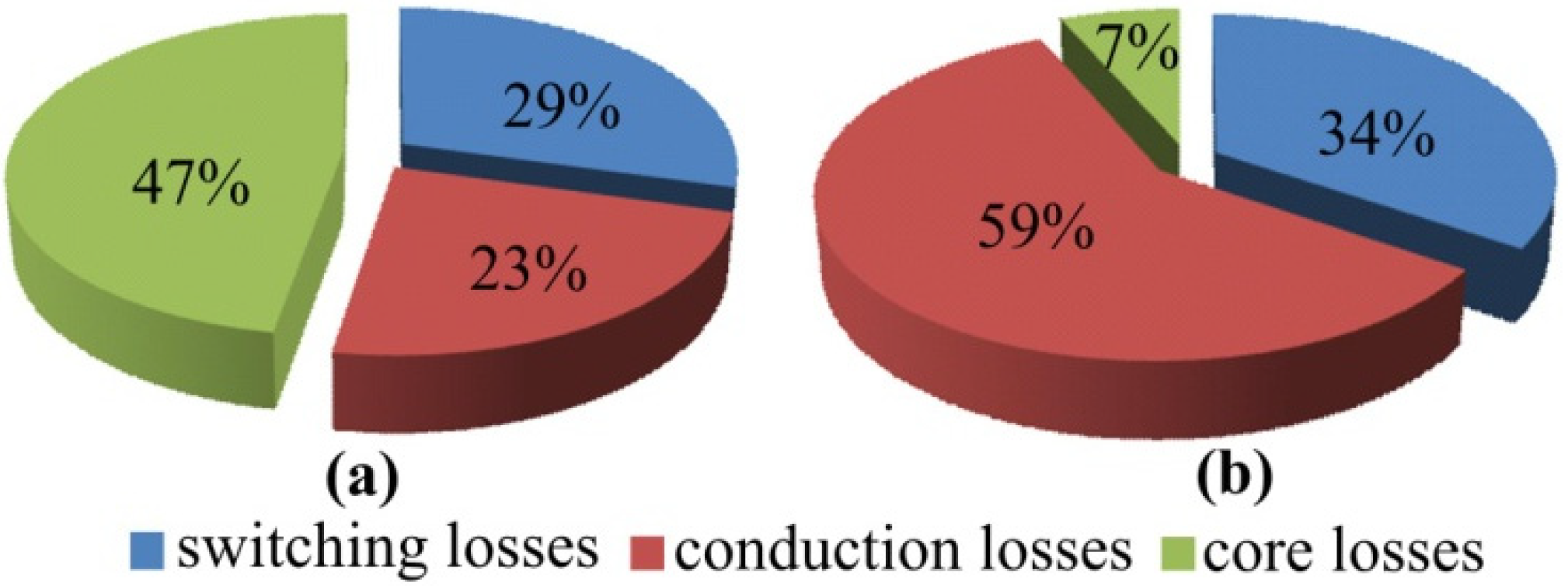
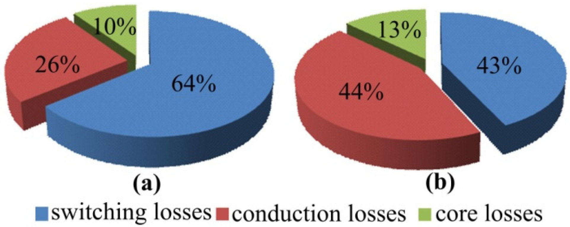
3.2. Losses Distributions Based on the Loss Analysis Model

The percentages of the three types of power loss are different, and they are functions of the load current. It is helpful to improve the efficiency of the PSFB converter by analyzing the loss distributions. The loss distributions for different currents can be obtained based on the loss analysis above, as shown in Figure 11 and Figure 12. Figure 11a shows the loss distribution under light load in CCM operation. It shows that the magnetic core losses make up almost half of the total losses. Figure 11b shows that the conduction losses are dominant under heavy load. Figure 12a,b show the loss distributions for different load conditions in DCM operation. Both of them show that the switching losses are dominant in DCM operation. The operating duty ratio reduces in DCM operation, resulting in the decrease of core losses because of lower flux swing.
Figure 11. Loss distribution in CCM operation (a) at 20% of full load; (b) at full load.
Energies 08 02647 g011
Figure 12. Losses distribution in DCM operation (a) at 1% of full load; (b) at 5% of full load.
Energies 08 02647 g012

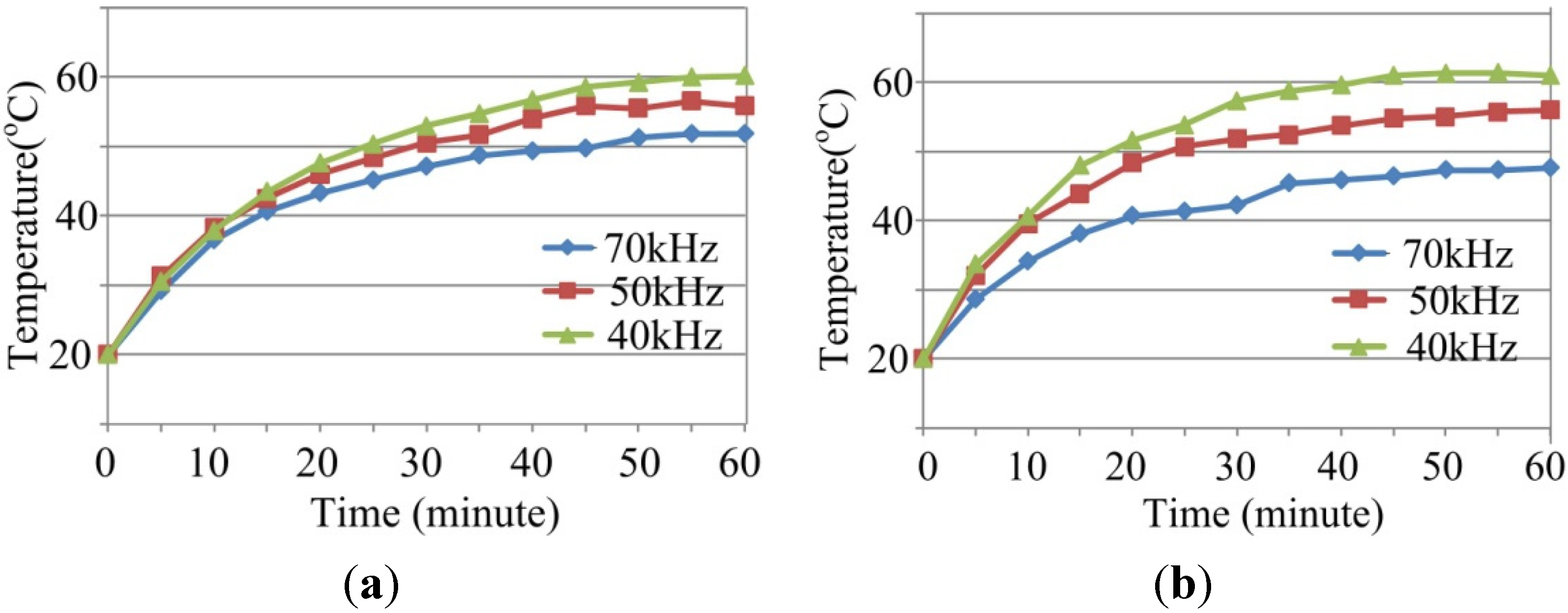
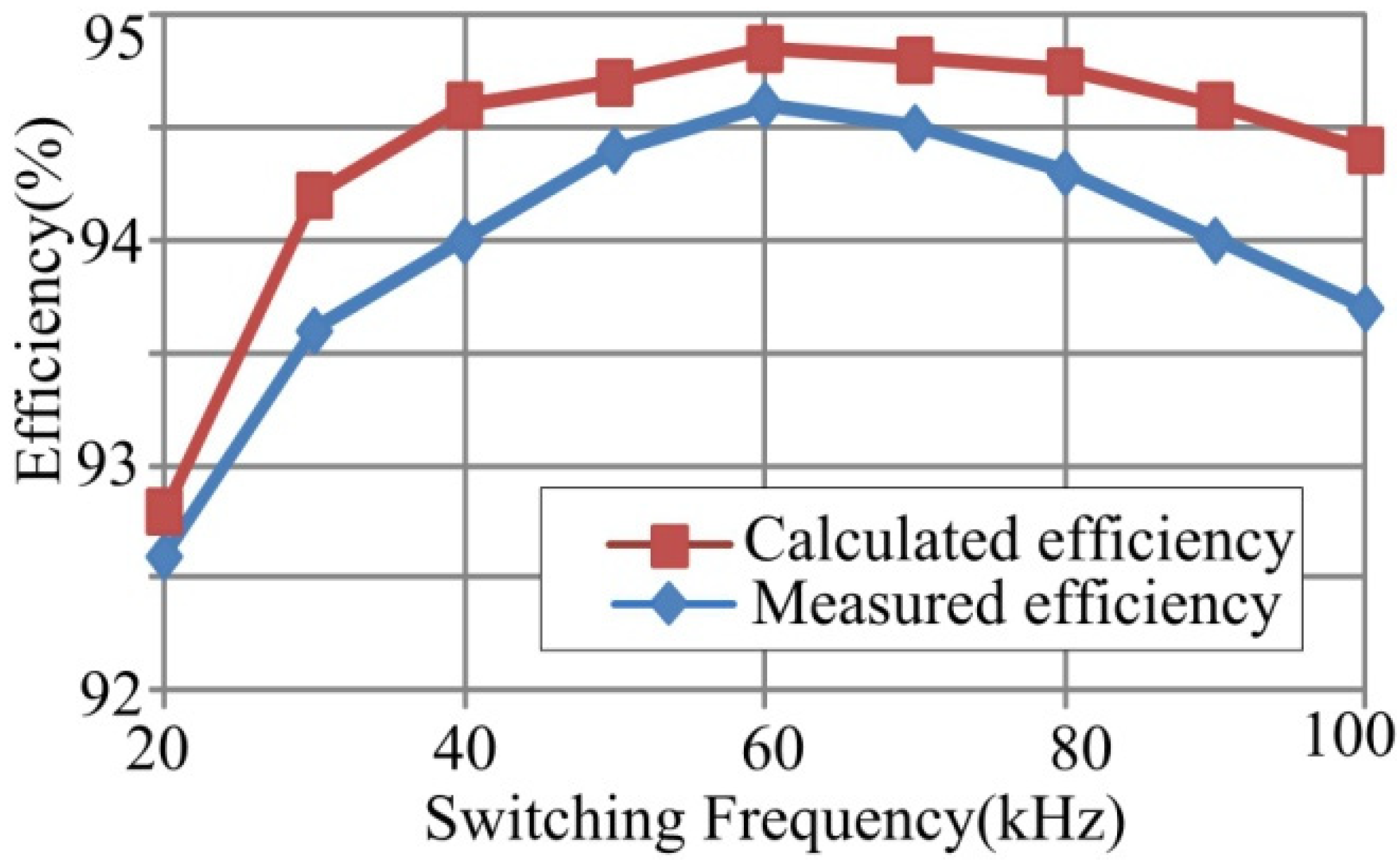
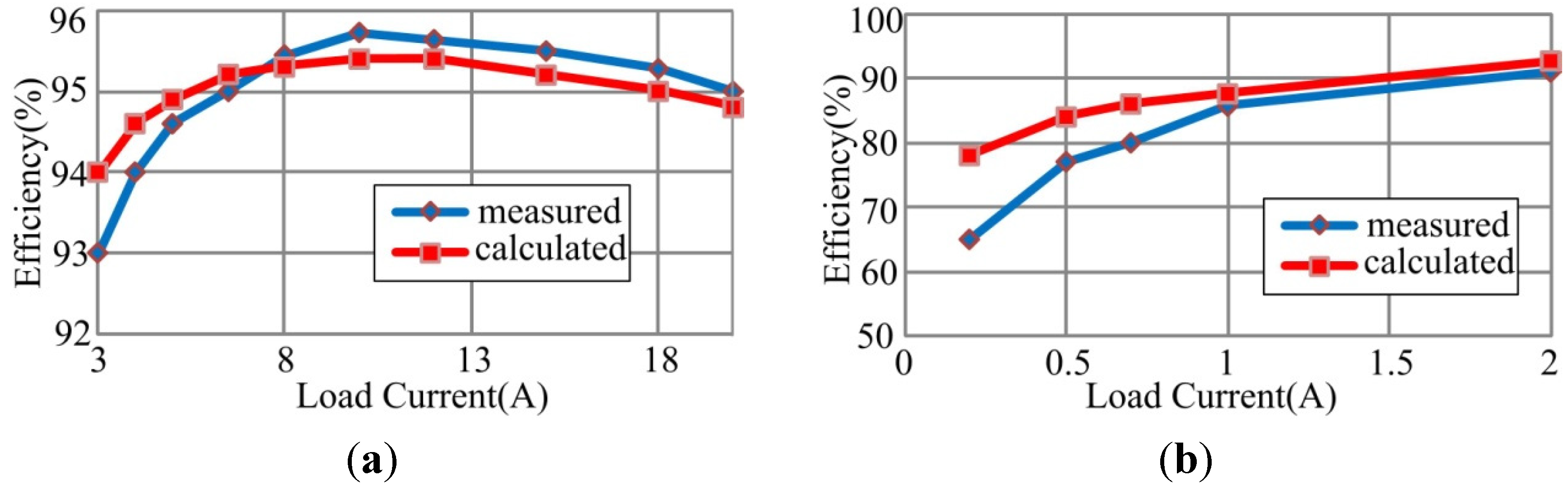
3.3. Experimental Efficiency Characterization

A prototype is implemented to validate the loss model. The specifications of the experimental system are shown in Table 1. The DSP TMS320F28027 is adopted for the digital control of PSFB converter. The minimum switching frequency is selected as 20 kHz, since the transformer will produce audio noise if the frequency is lower than 20 kHz. The maximum switching frequency is selected as 100 kHz in order to reduce the influence of limit cycle. The switching frequency is swept from 20 to 100 kHz with a 10 kHz step in order to obtain the efficiency data. Figure 13 shows the effect of switching frequency on the efficiency at Io = 5 A. The efficiency calculated based on the loss model coincides with the measured efficiency.
Table 1. Specifications of the converter.
ItemSymbolValue
Input VoltageVin400 V
Output VoltageVo48 V
Output CurrentIo20 A
Turns RatioNtr4
Filter InductorLo40 μH
MOSFETsQ1~Q4ST26NM60
Rectifier DiodesD1-D2STTH6002
Figure 13. Effect of switching frequency on the efficiency at Io = 5 A. Comparison of results based on the loss model and experiment.
Energies 08 02647 g013

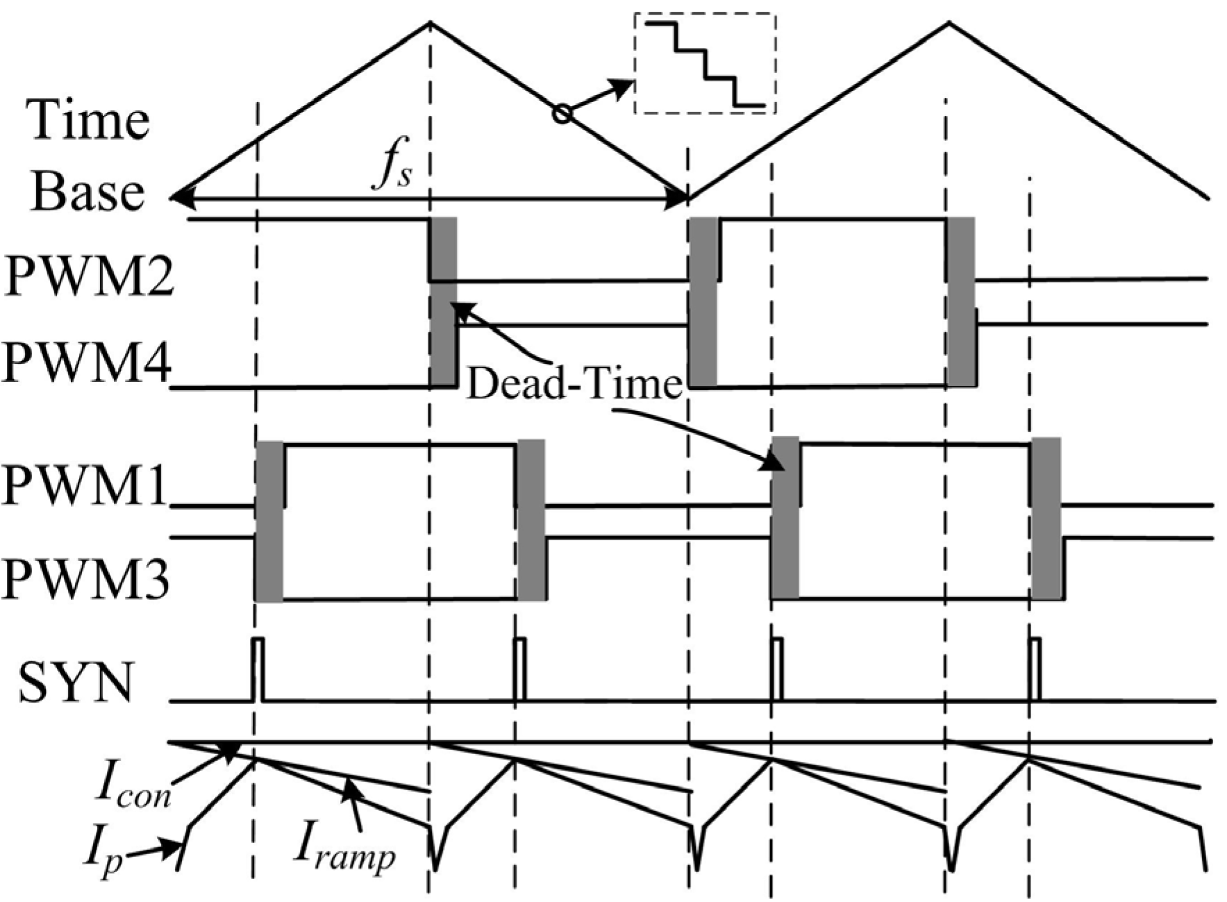
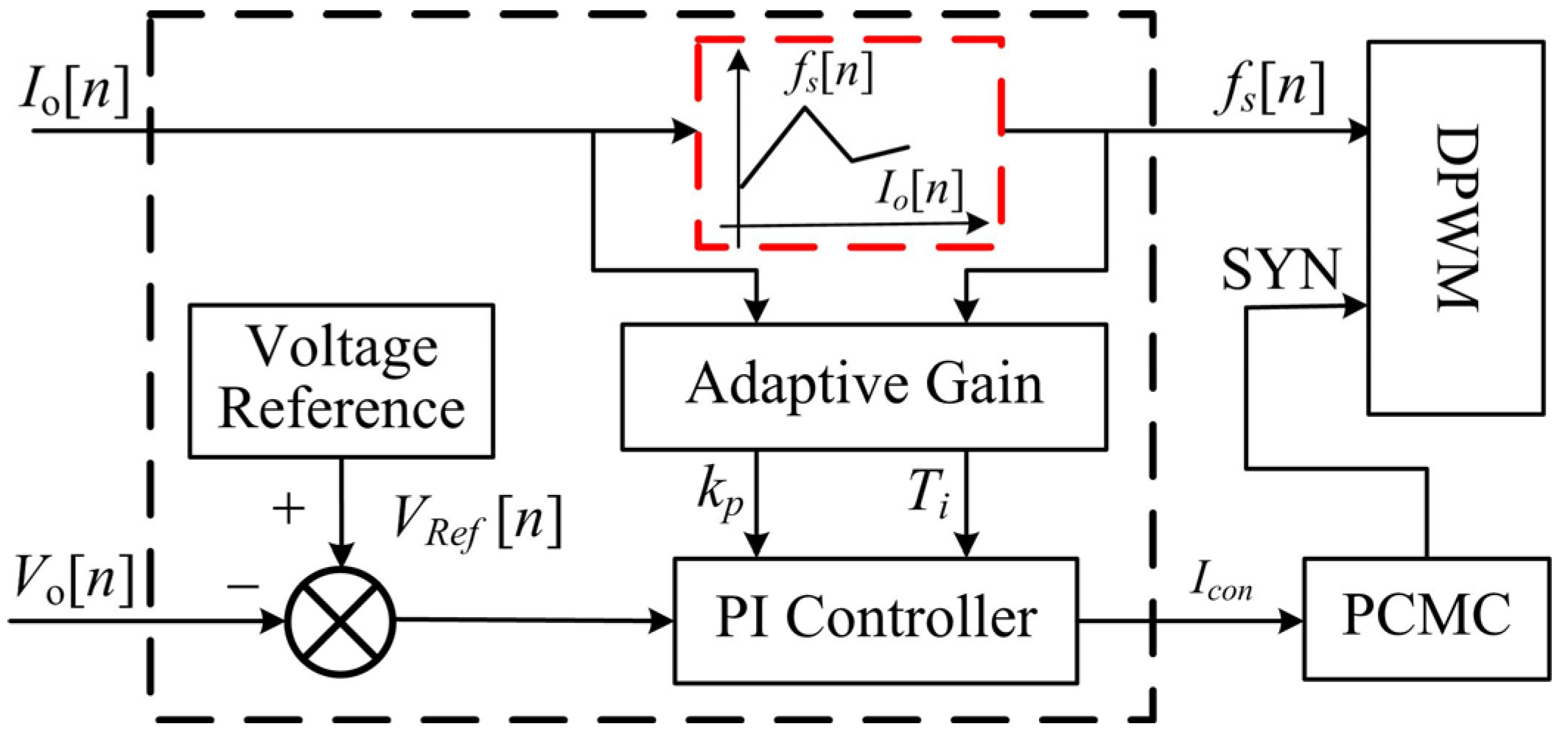
4. Control System with Load Adaptive Method

Lower switching frequency results in lower switching losses, but also results in higher conduction and magnetic core losses. Higher switching frequency leads to the opposite result. As the switching frequency is varied, one kind of loss increases and others decrease. For any specific load current, there is an optimum switching frequency which results in minimum total losses, as shown in Figure 9.

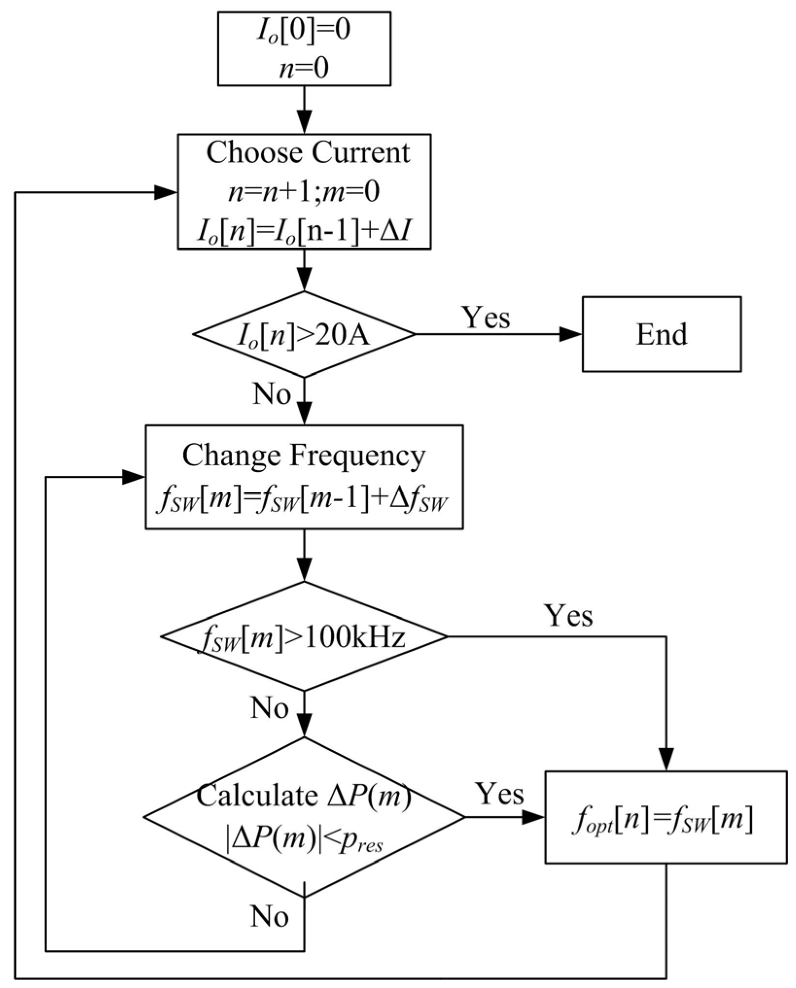
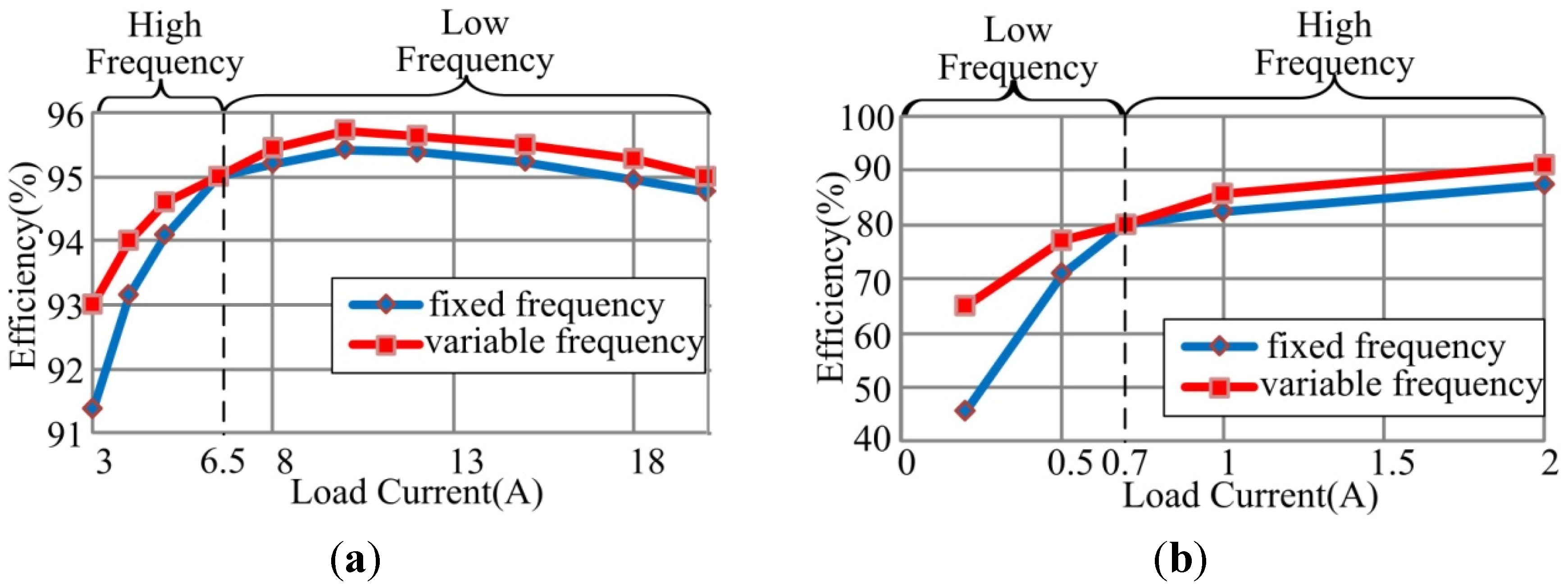
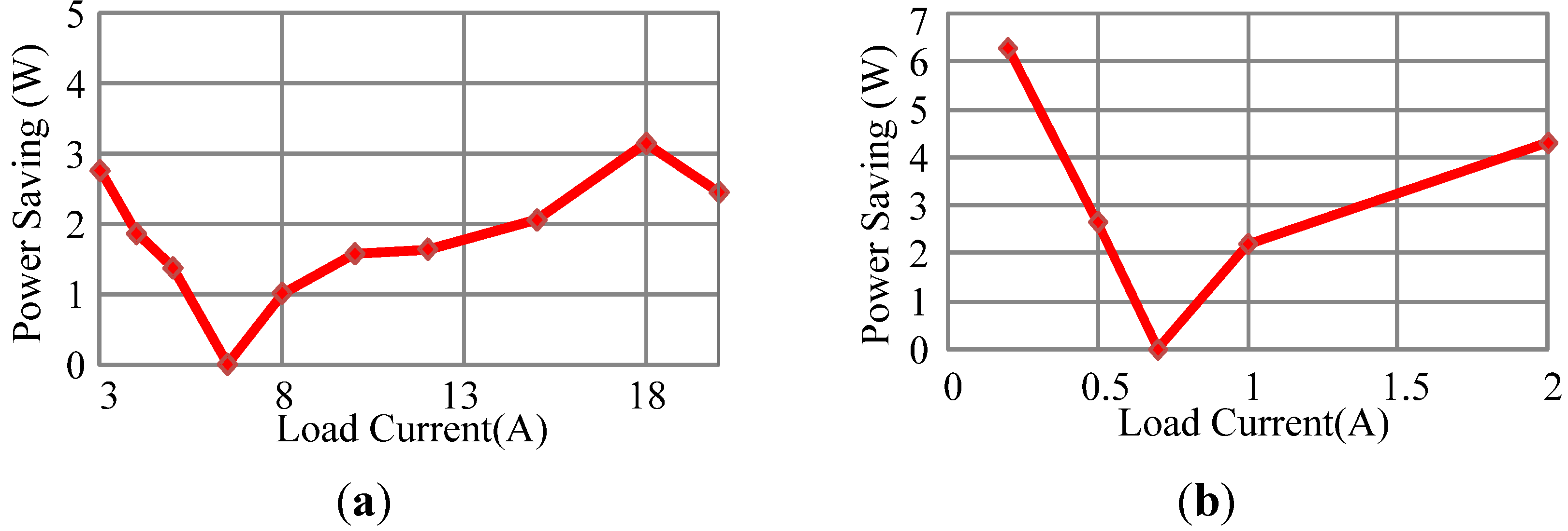
4.1. The Switching Frequency Optimization Procedure

By setting dη/df = 0, the optimum switching frequency can be obtained at different load currents. However, the efficiency model is very complex and it is difficult to obtain the solution. The following iteration equations can be used to obtain the optimum switching frequencies at different load currents:
I o ( n ) = I o ( n 1 ) + Δ I o
f S W ( n ) = f S W ( n 1 ) + Δ f S W
Δ P ( n ) = P T o t a l [ I o ( n ) , f S W ( n ) ] P T o t a l [ I o ( n ) , f S W ( n 1 ) ]
where the increment current step size ΔIo is 0.05 A; the increment switching frequency step size ΔfSW is 100 Hz.
The maximum and minimum value of the load current Io[n] is 20 A and 0.1 A, respectively. The maximum and minimum value of the switching frequency fSW[n] is 100 kHz and 20 kHz, respectively. The resolution of power loss pres is 0.2 W. If ΔP(n) is less than –pres, fSW should be incremented by ΔfSW to move toward the minimum power loss. If ΔP(n) is greater than pres, fSW should be decreased by ΔfSW. When ΔP(n) is between –pres and pres, this indicates the effect of switching frequency on total power loss can be neglected and fSW[n] can be regard as the optimum switching frequency under Io[n] load conditions. Figure 14 shows the flowchart of the switching frequency optimization procedure.
Figure 14. Block diagram of the switching frequency optimization procedure.
Energies 08 02647 g014
Figure 15 shows the optimum switching frequency fopt[n] at different load currents. It shows that fopt[n] increases with load current under light loads. Core losses make up almost half of the total losses under light loads since they are almost independent of the load. Higher switching frequency results in lower conduction losses, lower magnetic core losses and higher efficiency. At mid-range loads, fopt[n] decreases while load current increases. When the load current increases, the percent of the magnetic core losses decreases. The switching losses decrease with the switching frequency while the conduction losses increase because of higher ripple and rms current. However, the ripple current is very small compared with the load current under mid-range and heavy loads. The increase of rms current caused by the decrease of switching frequency can be ignored, so the efficiency increases while switching frequency decreases under mid-range loads.
Figure 15. Optimum switching frequency at different load currents.
Energies 08 02647 g015
However, a lower switching frequency means a lower power density when the converter transfers the same power. The following formula provides a crude indication of the area product required [16]:
A P = ( P o K Δ B f s ) 4 / 3
where AP is a constant value determined by the size of the magnetic core; Po means output power, K = 0.17 for the PSFB converter. Based on Equation (45), the minimum switching frequency fsmin can be obtained for different load currents, just as shown in Figure 15. Therefore, under heavy loads, fopt[n] is set by fsmin which is decided by the output power. The red dashed curve means the optimum switching frequency without the constraint of the minimum switching frequency when the load current is greater than 15 A.

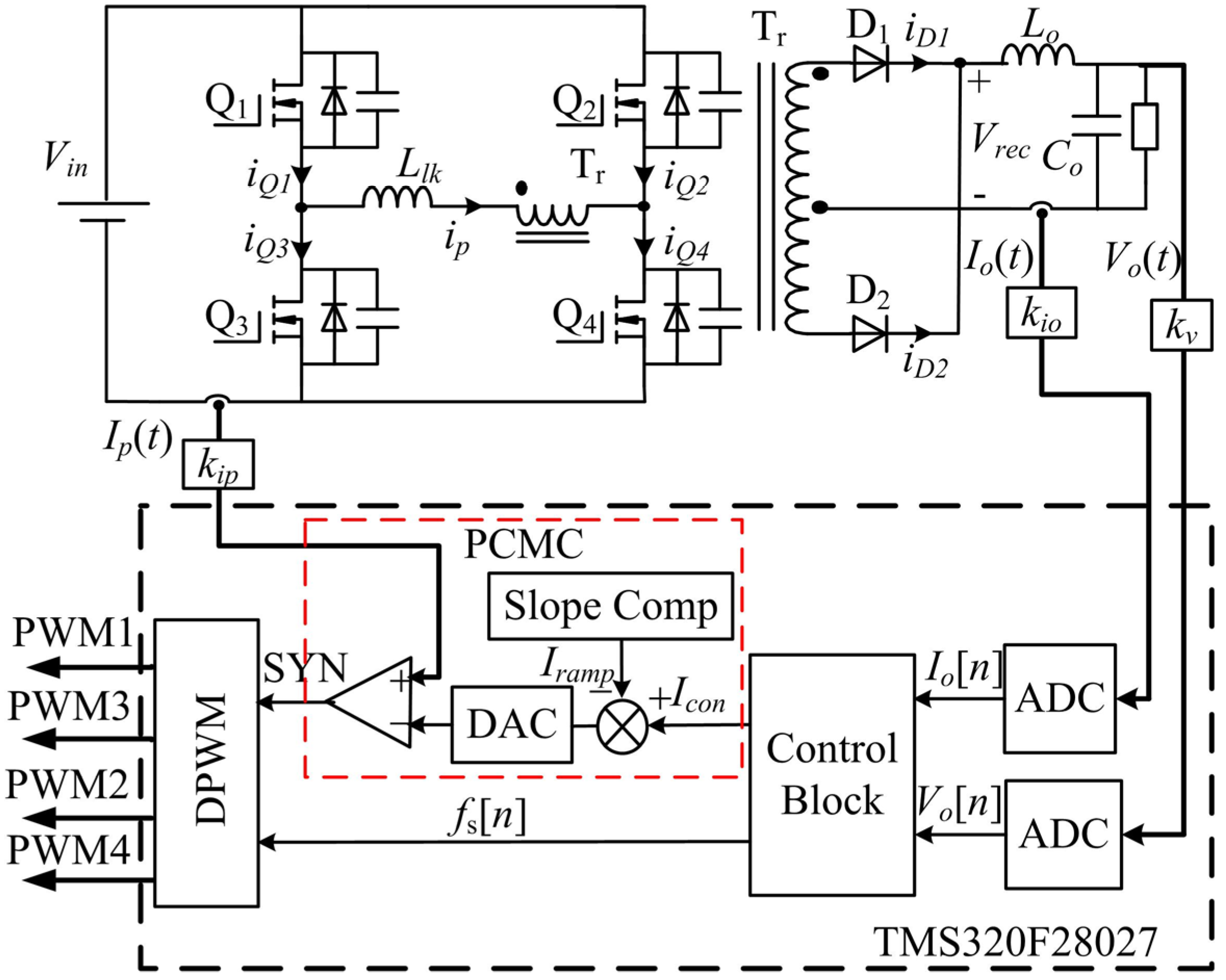
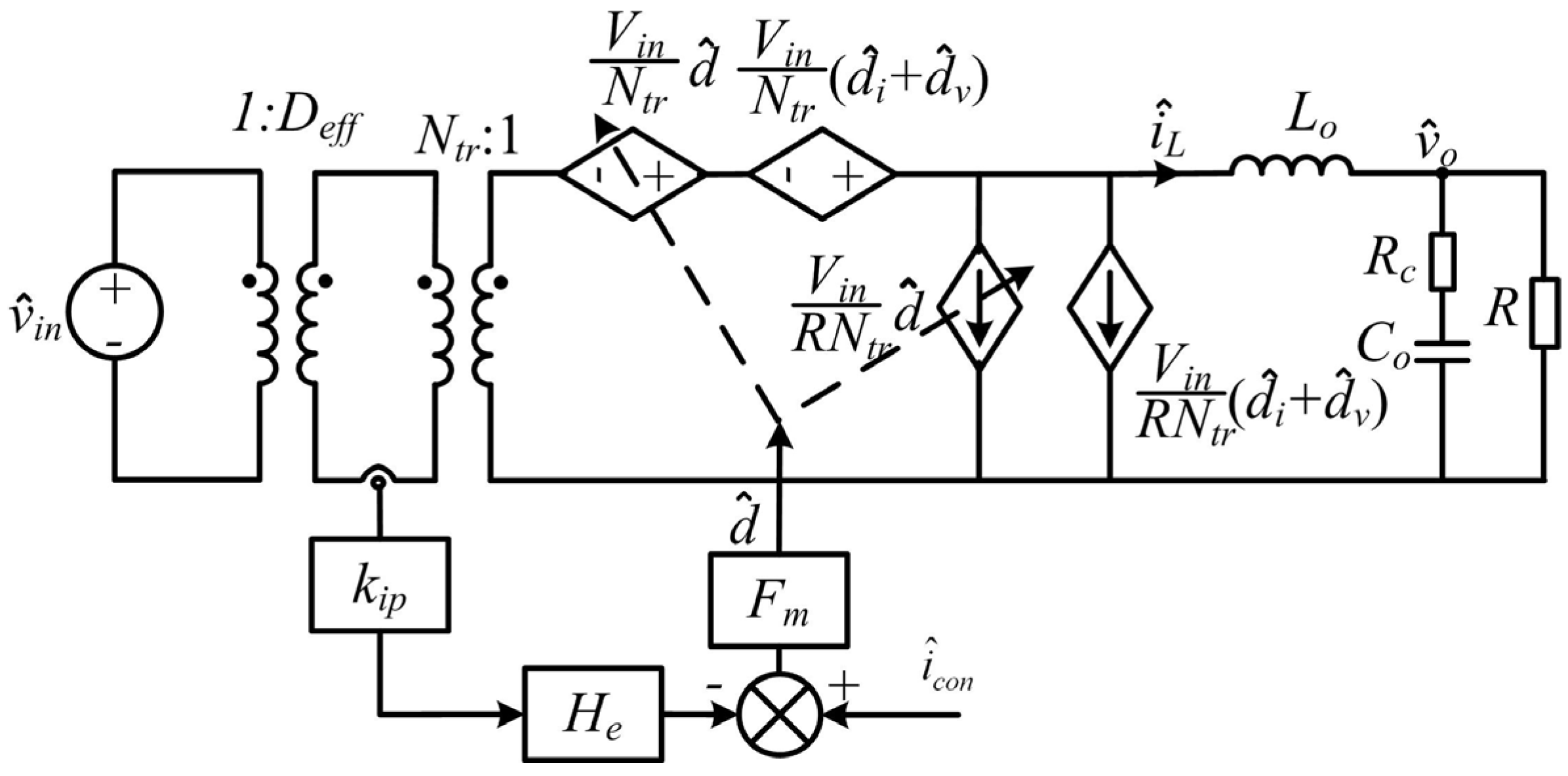
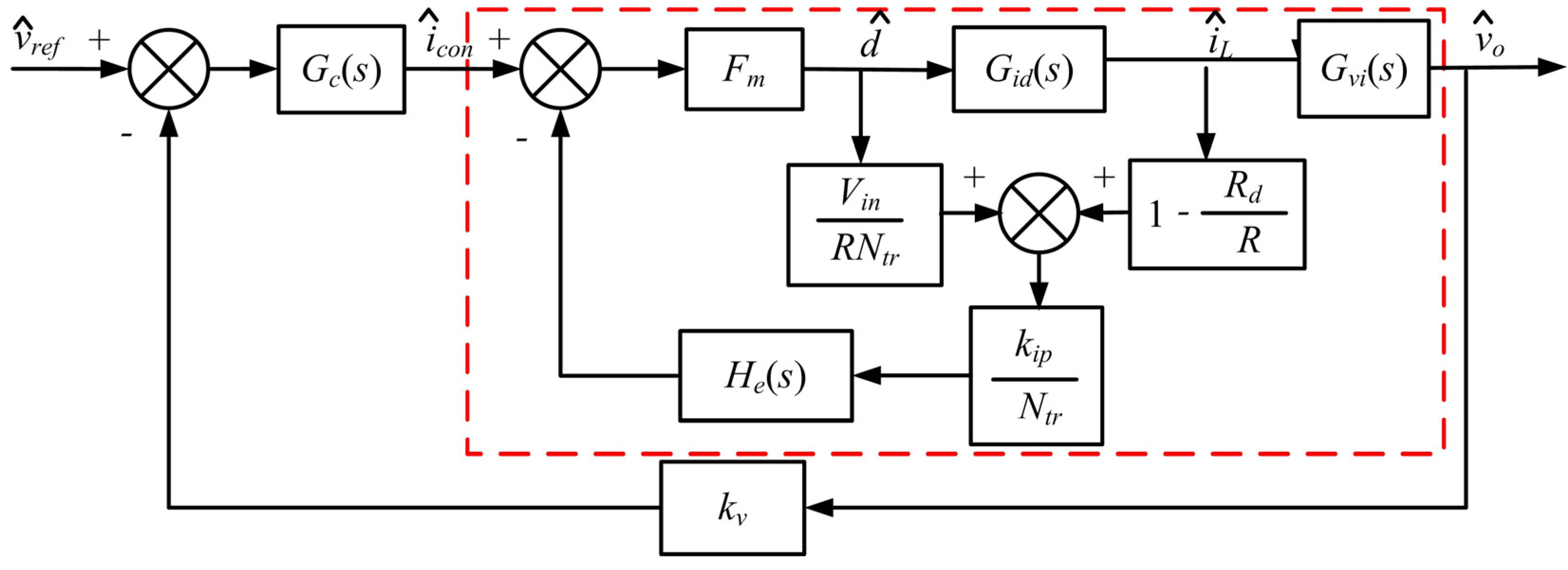
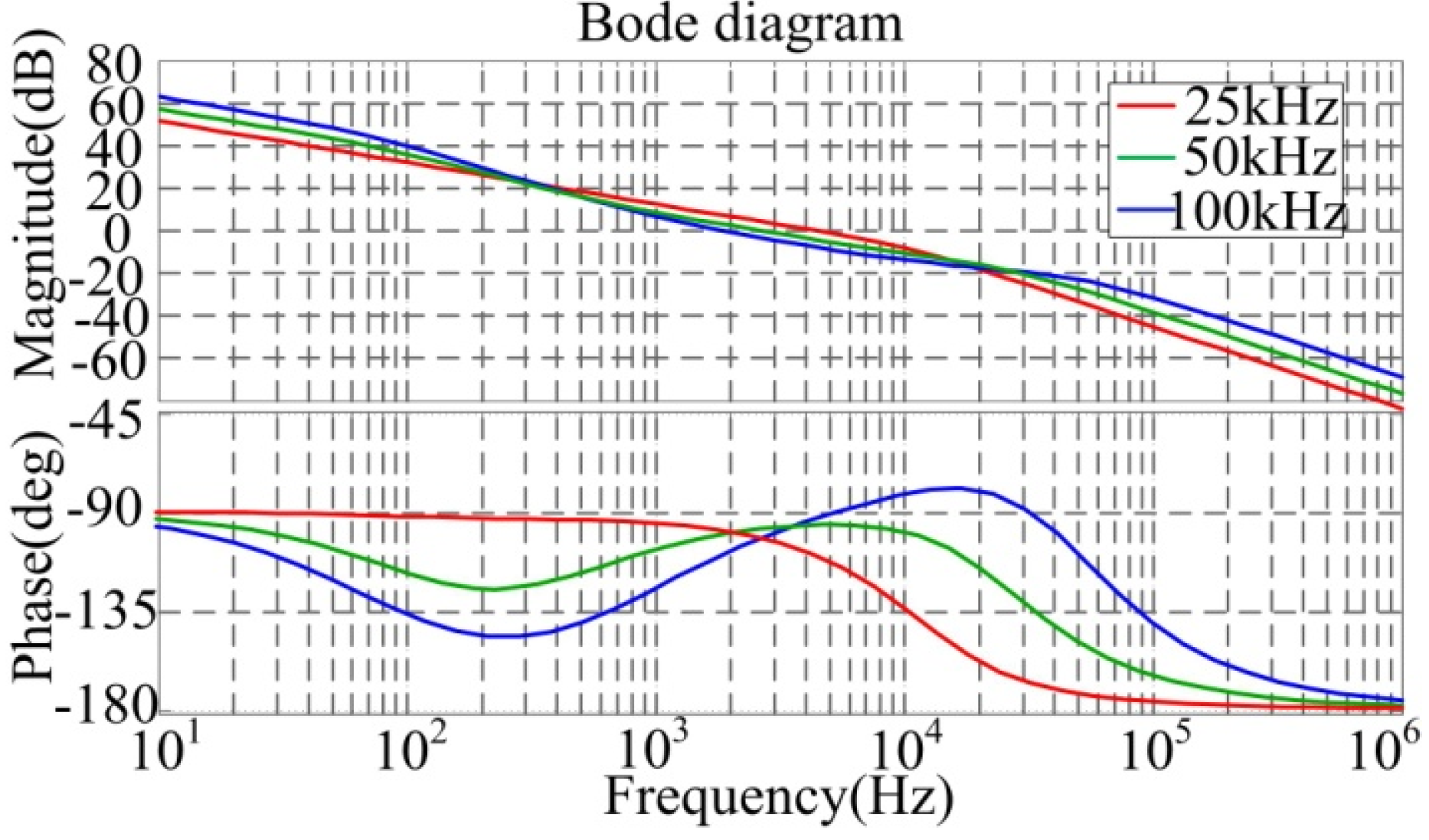
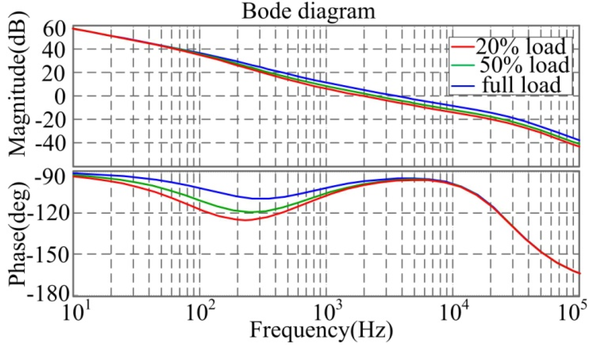
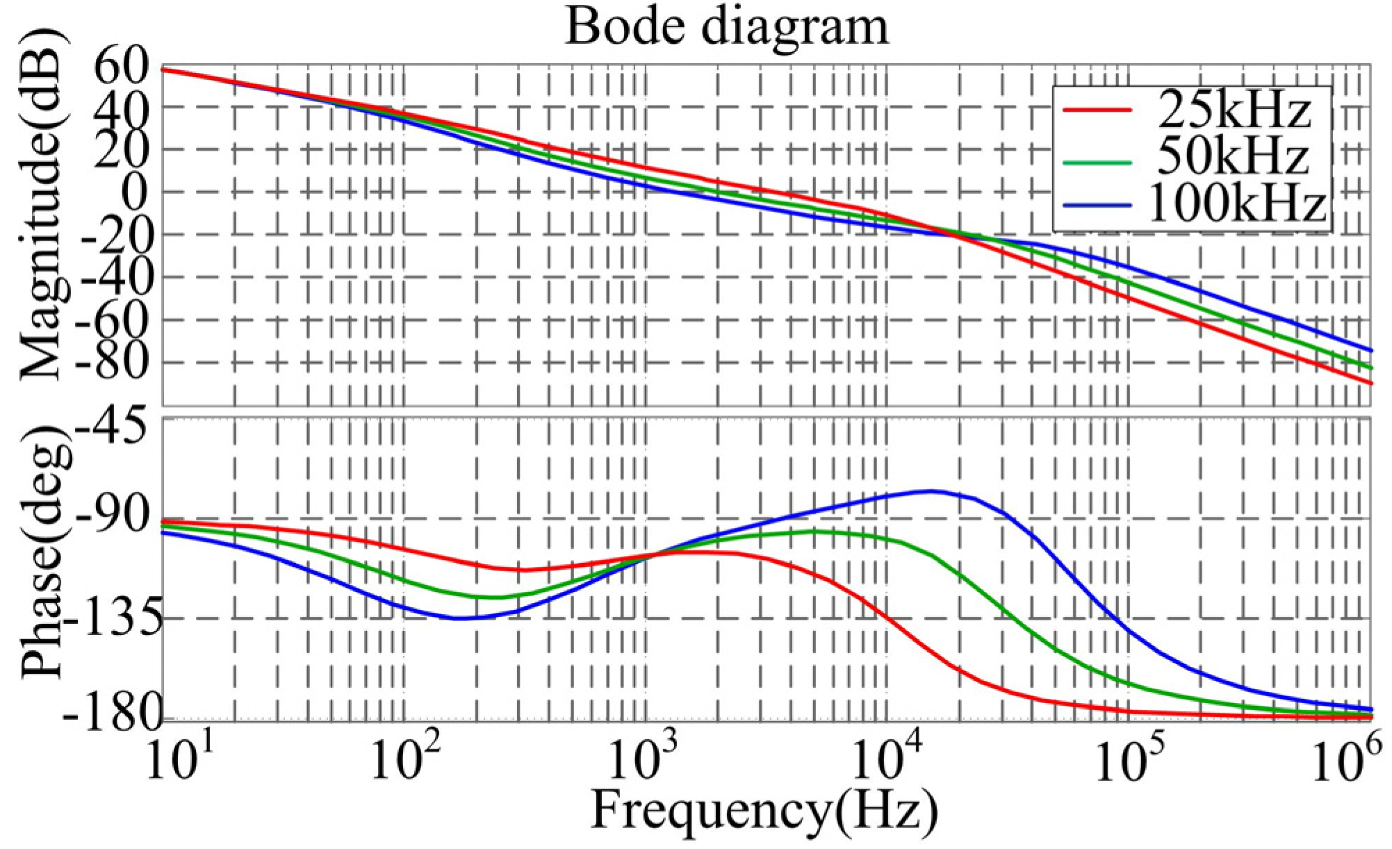
4.2. The Proposed Closed Loop Control System

In the PSFB converter, flux bias in the transformer is generated because of the differences between the devices [24]. This problem affects the proper operation of the converter. Peak current mode control (PCMC) is an effective way to solve this problem. This approach can balance the transformer flux in an isolated converter, improve the dynamic response and simplify the controller design [24,25,26]. PCMC has been widely adopted in switch mode power supplies.
Figure 16 shows the proposed closed-loop control system. The control system is implemented in the DSP TMS320F28027 manufactured by Texas Instruments (Dallas, TX, USA) It consists of A/D conversions, control block which will be described in detail below (see Figure 24), PCMC control block and digital PWM module. PCMC is unstable and undesirable sub-harmonic oscillations occur whenever the steady-state duty cycle is greater than 0.5. To ensure the converter stability, slope compensation is added. As shown in Figure 16, the PCMC control block includes an on-chip analog comparator, digital to analog converter and slope compensation. Slope compensation adds a ramp signal Iramp with a negative slope to the peak current reference signal Icon which is calculated by the control block. Primary current is compared with the slope compensated peak current reference using the on-chip analog comparator. In Figure 16, kip, kio and kv are the linear gains of the sensor network.
Figure 16. Closed-loop system block diagram.
Energies 08 02647 g016
Figure 17 shows the PWM signal generation with PCMC. When the time-base counter equals the period, PWM2 is at low level and PWM4 is at high level after a dead-time window. PWM4 is at low level and PWM2 is at high level after a dead-time window while the time-base counter is equal to the zero. When the primary current reaches Icon in every half of the switching cycle, and one of the PWM waveforms driving the switches (Q1/Q3) changes to low level immediately. The PWM waveform driving the other switch in the same leg changes to high level after a dead-time window.
Figure 17. PWM signal generation with PCMC.
Energies 08 02647 g017

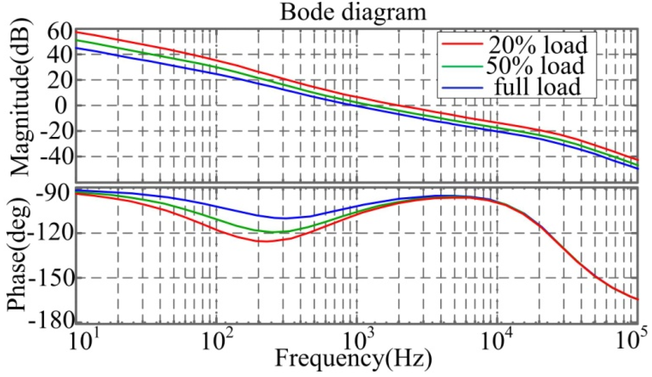
4.3. Design of the Adaptive Gain Adjustment Controller

According to Equations (2)–(4), the effective duty cycle Deff depends not only on the duty cycle D of the primary voltage, but also on the input voltage Vin, the output inductor current IL, the leakage inductance Llk, and the switching frequency fs. Therefore the small-signal transfer function of the PSFB converter will depend on Llk, fs; and the perturbations of duty cycle of primary voltage d ^ ; input voltage v ^ i n ; and output inductor current i ^ L . The small-signal circuit model of the PSFB converter with PCMC is shown in Figure 18 [18,25]. The variables in Figure 18 are defined as follows:
  • d ^ i : the perturbation of duty cycle caused by i ^ L ;
  • d ^ v : the perturbation of duty cycle caused by v ^ i n ;
  • i ^ c o n : the perturbation of peak current reference;
Four dependent sources represent the contributions of d ^ i , d ^ v and d ^ . Additionally, d ^ i and d ^ v are expressed by the following formulas:
d ^ i = N t r R d V i n i ^ L , d ^ v = N t r R d I L V i n 2 v ^ i n , R d = 4 L l k f s N t r 2
He is used to model the sampling action of PCMC and the transfer function can be represented as [26]:
H e ( s ) 1 1 2 f s s + ( 1 π f s ) 2 s 2
The red outline in Figure 16 shows the PCMC modulation scheme. The modulator gain can be expressed as:
F m = f s ( S n + S e ) = f s m c S n , m c = 1 + S e S n
where Sn is the slope of the input current-sense waveform when energy is being delivered to the secondary side and Se is the compensation slope.
Figure 18. Small-signal circuit model of the converter with PCMC.
Energies 08 02647 g018
Figure 19 shows the block diagram of the control closed-loop. In Figure 19, Gid(s) and Gvi(s) can be derived based on the small-signal circuit model shown in Figure 18. Gc(s) is the PI voltage controller:
G c ( s ) = k p ( 1 + 1 T i s ) = k p T i T i s + 1 s
According to Figure 19, the approximate control-to-output transfer function for the PSFB converter with PCMC is given by [27]:
G v c ( s ) = v ^ o i ^ c o n = N t r V o k i p I o F p ( s ) F h ( s )
where F p ( s ) = 1 + s C o R c 1 + s / ω p ; ω p = 1 C o R + 1 L o C o f s ( m c D 0.5 ) ; D = 1 D ; F h ( s ) = 1 1 + s ω n Q + s 2 ω n 2 ; ω n = π f s ; Q = 1 π ( m c D 0.5 ) .
Figure 19. Block diagram of the control closed-loop. The block diagram in the red outline represents control-to-output transfer function.
Energies 08 02647 g019
The open-loop control transfer T(s) can be expressed as follows:
T ( s ) = k v G c ( s ) G v c ( s )
The desired crossover frequency and phase margin of the compensated open-loop transfer function T(s) can be achieved by adjusting PI controller parameters kp and Ti. The crossover frequency of T(s) is selected as 2 kHz with a phase margin of 80 degree at output current Io = 4 A. The switching frequency f0 is 50 kHz under this specific operation condition. The PI controller is expressed as follows:
G c ( s ) = k p 0 ( 1 + 1 T i 0 s ) = 4.43 ( 1 + 1 3.6 e 4 s )
The digital controller is designed using a digital redesign approach. First, the PI controller is devised in the continuous s-domain, as Equation (53). Second, by using a Backward-Euler transformation (a discretization method) [28,29], the controller in the discrete z-domain can be calculated as:
G z c ( z ) = k p T S a m p l e T i T S a m p l e / T i ( 1 z 1 ) + 1 1 z 1
where TSamp is the sampling period. Switching transitions for switches may cause some disturbance on the sampled signals. To avoid this disturbance, the signals are sampled at the midpoint of the PWM signal, i.e., as far away from the switching transitions as possible, so the sampling period is set the same as switching period.
According to Equations (50)–(52), the gain of the open-loop transfer function T(s) can be calculated as:
| T ( s ) | = k p k v N t r V o k i p I o T i
Based on Equations (54) and (55), the gains of the PI digital controller Gzc(z) and open-loop transfer function T(s) are different when the load current or switching frequency vary. Figure 20 and Figure 21 show the frequency responses of T(s) with different currents and switching frequencies, respectively.
It can be noted that the magnitude of T(s) in the low frequency zone varies with the load current and switching frequency. This problem results in degradation in the dynamic performance of the converter control. As shown in Figure 20 and Figure 21, the fixed controller parameters are not suitable for different operation conditions. The controller parameters need to be adjusted according to the particular load conditions. To address a wide range of load conditions, an adaptive gain adjustment technology is adopted in this paper. In order to obtain the same magnitude of T(s) in the low frequency zone when the load current or switching frequency vary, the gains of Gzc(z) and T(s) should be constant. The modified parameters of the PI controller can be calculated based on Equations (54) and (55):
T i = T i 0 f 0 f s , k p = k p 0 I o T i I o T i 0
Figure 22 and Figure 23 are the frequency responses of the open-loop transfer with adaptive gain adjustment. The proposed controller adjusts Ti and kp based on Equation (56). As shown in Figure 22 and Figure 23, the frequency responses of T(s) have approximately the same magnitude in the low frequency zone although the load current or switching frequency vary.
Figure 20. Frequency response of T(s) under different load conditions.
Energies 08 02647 g020
Figure 21. Frequency response of T(s) under different switching frequencies.
Energies 08 02647 g021
Figure 22. Frequency response of T(s) under different load currents with the adaptive controller.
Energies 08 02647 g022
Figure 23. Frequency response of T(s) under different frequencies with the adaptive controller.
Energies 08 02647 g023

4.4. Control Block Diagram of the Proposed Method

To obtain high efficiency over a wide range of load conditions, the switching frequency must be adaptively adjusted according to the load current. The fixed controller parameters do not satisfy the set specifications in the frequency domain while the load current or switching frequency vary widely. This problem results in degradation of the dynamic performance of the converter control. The controller parameters need to be adjusted adaptively. In this paper, a load adaptive control method is presented to adjust the switching frequency and controller parameters according to the load conditions. Figure 24 shows the control block diagram of the proposed approach. As shown in Figure 16, the control block is a part of the closed-loop system block. There are two control loops according to Figure 24. The first control loop determines the peak current reference Icon to regulate the output voltage. The second control loop adjusts the switching frequency according to the load current. A lookup table is employed to realize the optimum switching frequency. This table is built based on Figure 15. The adaptive-gain block determines the PI controller parameters. The parameters are calculated based on Equation (56).
Figure 24. Control block diagram of the proposed method.
Energies 08 02647 g024

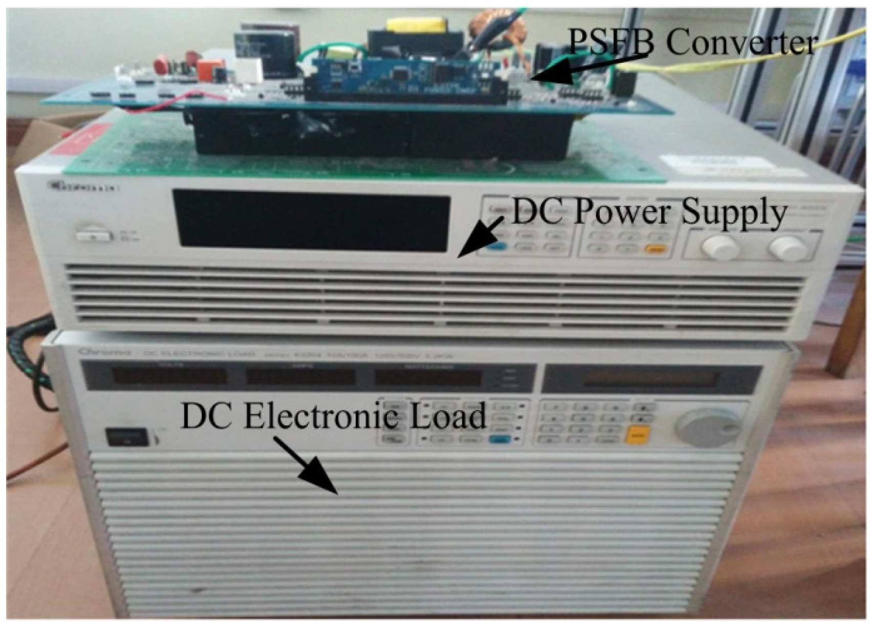
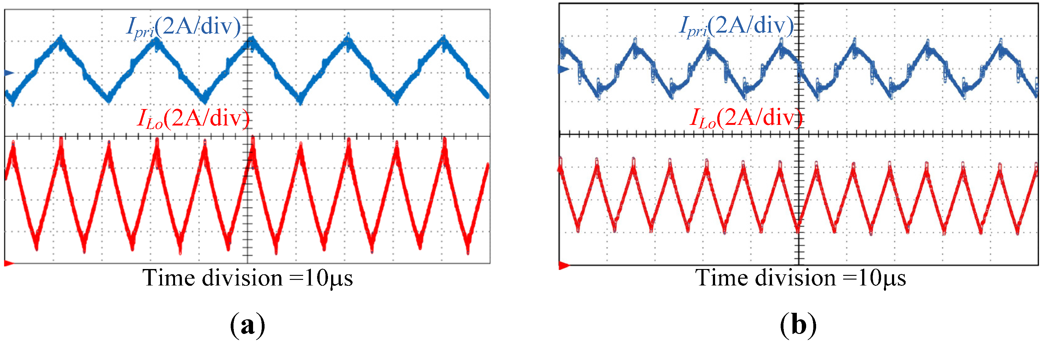
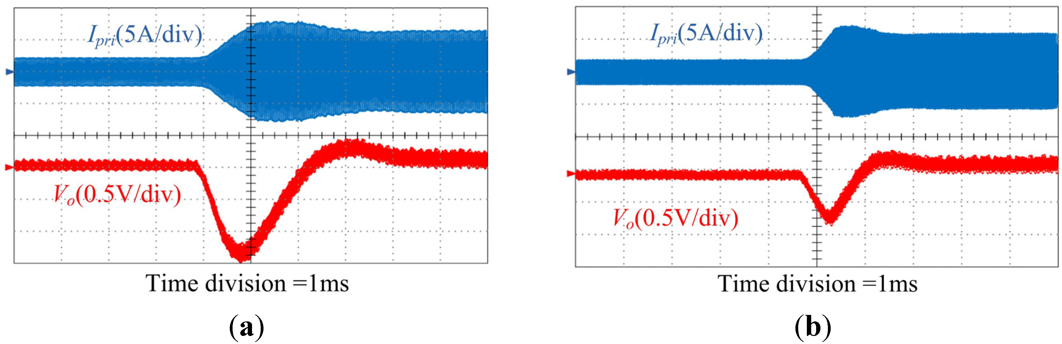
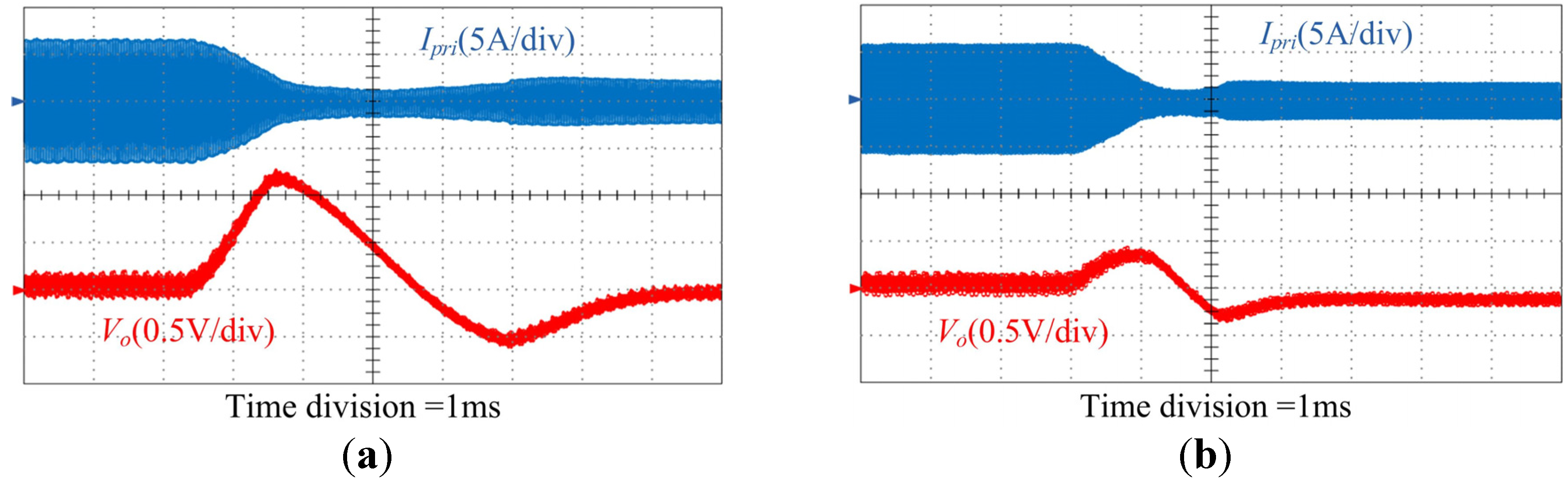
5. Experimental Results

A prototype is implemented to verify the proposed control method. The specifications of experimental system are shown in Table 1. The switching frequency of conventional fixed-frequency converter is constant 50 kHz. In order to obtain high efficiency under a wide range of load conditions, the switching frequency of the proposed converter varies with the load current according to the optimum switching frequency curve fopt in Figure 15. The proposed method is suitable for the converter which has been designed based on the fixed frequency design procedure, so the proposed method can improve conventional converters without any additional components. A picture of the laboratory setup is shown in Figure 25. The input power is evaluated through a 62150H DC Power Supply and the output power is measured through a DC Electronic Load 63204. Both of the devices are manufactured by the Chroma Company (Bellows Falls, VT, USA).
Figure 25. Picture of the laboratory setup.
Energies 08 02647 g025
Figure 26 shows the experimental waveforms of magnetic components currents with the conventional control method and proposed control method at Io = 4 A. The switching frequency of the conventional converter is 50 kHz while it is 65 kHz for the proposed converter. By comparing Figure 26a with Figure 26b, it can be noted that the peak-to-peak value of primary current Ipri and output filter inductor current ILo with the proposed method are lower than those obtained with the conventional method. A lower peak-to-peak value results in a lower flux swing and core losses. Core losses of magnetic components are almost independent of the load, and make up almost half of the total losses under light loads, so the proposed converter with higher switching frequency can achieve higher efficiency. The measured efficiency with variable frequency is 94% while that with fixes frequency is 93.1%. The experimental result coincides with the analysis result.
Figure 26. Current waveforms of magnetic components currents under 20% of full load (a) Conventional converter at fs = 50 kHz; (b) Proposed converter at fs = 65 kHz.
Energies 08 02647 g026
Figure 27 shows the dynamic responses of the converter for a load step transient before and after applying the adaptive PI controller when the load changes from 20% (4 A) to 100% (20 A) of the rated load. It can be noted that the adaptive PI controller results in lower output voltage undershoot and faster dynamic response. Figure 28 presents waveforms for a load step down transient (20 A–4 A) before and after applying the adaptive PI controller. Comparison between Figure 28a,b indicates that the dynamic responses of Vo are much improved with the proposed adaptive PI controller.
Figure 27. Dynamic responses of the converter for load step transient (4 A–20 A). (a) Using conventional PI controller; (b) Using adaptive PI controller.
Energies 08 02647 g027
Figure 28. Dynamic responses of the converter for load step transient (20 A–4 A). (a) Using conventional PI controller; (b) Using adaptive PI controller.
Energies 08 02647 g028
Figure 29 shows the calculated maximum efficiency and the measured efficiency of the converter with the proposed variable frequency control method. Because of the wide range of load conditions, Figure 29a shows the efficiency curves under mid-range and heavy loads and the efficiency curves under light loads are shown in Figure 29b. The calculated efficiency based on the loss analysis model almost coincides with the measured efficiency under a wide range of load conditions.
Figure 29. Calculated efficiency versus measured efficiency at different loads. (a) Efficiency curves under mid and heavy loads; (b) Efficiency curves under light loads.
Energies 08 02647 g029
Figure 30 shows a comparison of the efficiency between the fixed-frequency control method and the proposed variable-frequency control method. Figure 31 shows the energy savings achieved by adopting the proposed control method. The proposed method indeed achieves higher efficiency over a wide range of load currents compared to the fixed-frequency control method due to the fact that the switching frequency varies according to the load current. The light-load efficiency improvement can be up to 20% since switching losses are dominant under light loads and it can be greatly reduced by adopting variable frequency modulation.
Figure 30. Efficiency comparison between the fixed frequency control and variable frequency control (a) at mid and heavy loads; (b) at light loads.
Energies 08 02647 g030
Figure 31. Energy saving by adopting the proposed control method (a) at mid and heavy loads; (b) at light loads.
Energies 08 02647 g031
The optimum switching frequency is lower than the fixed-frequency when the load current is lower than 0.7 A. The efficiency is primarily determined by switching losses when the load current is below 5% of the full load, as illustrated in Figure 12. When the load current is between 0.7 A to 6.5 A (about 5% to 30% of the full load), magnetic component losses make up almost half of the total losses. The optimum switching frequency is higher than the fixed-frequency. Higher switching frequency results in lower conduction losses and lower magnetic core losses. Furthermore, as the output power of the converter increases, the optimum switching frequency is lower than the fixed-frequency. Lower switching frequency results in lower switching losses, but results in higher conduction losses and core losses. However, the ripple current is very small compared with load current and magnetic core losses are almost independent of the load under CCM operation. The increased core losses and conduction losses caused by the decease of the switching frequency can be ignored under mid-range and heavy load conditions.

6. Conclusions

In this paper, three types of power loss for the PSFB converter are discussed in detail and the loss analysis model is presented. In addition to introducing the effect of the switching frequency on efficiency, the efficiencies for different switching frequencies are also measured experimentally. The measured efficiencies coincide with the efficiencies calculated based on the loss model.
By analyzing the loss model, the optimum switching frequency which results in minimum total losses varies with the load current. The proposed iteration equations can be used to obtain the optimum switching frequency for different load currents. Based on the relationship between the optimum switching frequency and load current, the converter can achieve the optimum switching frequency over a wide range of load currents, and the experimental results show that the efficiency can be improved under a wide range load conditions and the maximum improvement can be up to 20%.
Moreover, the magnitude of the open-loop transfer function at low frequency zone varies with load current and switching frequency. This problem results in degradation in the dynamic performance of the converter control. By adjusting the controller parameters, the gain of the open loop transfer function can have approximately the same magnitude at low frequency zone which makes the converter achieve a faster dynamic response. The theoretical analysis and experimental results show that the efficiency and dynamic performance are improved with the proposed control method.

Acknowledgments

This work was supported by National Natural Science Foundation (Grant No. 51074056) and Delta Environmental & Educational Foundation (Grant No. DREG2011006).

Author Contributions

Lei Zhao was responsible for the theoretical derivation and paper writing. Haoyu Li proposed the main idea and analysis method. Yuan Liu and Zhenwei Li carried out the simulation and verification.

Conflicts of Interest

The authors declare no conflict of interest.

References

  1. Kim, Y.D.; Cho, K.M.; Kim, D.-Y.; Moon, G.-W. Wide-range ZVS phase-shift full-bridge converter with reduced conduction loss caused by circulating current. IEEE Trans. Power Electron. 2013, 28, 3308–3316. [Google Scholar] [CrossRef]
  2. Shi, X.; Jiang, J.; Guo, X. An efficiency-optimized isolated bidirectional DC-DC converter with extended power range for energy storage systems in microgrids. Energies 2013, 6, 27–44. [Google Scholar] [CrossRef]
  3. Zhang, S.; Zhang, C.; Xiong, R.; Zhou, W. Study on the optimal charging strategy for lithium-ion batteries used in electric vehicles. Energies 2014, 7, 6783–6797. [Google Scholar] [CrossRef]
  4. Shiau, J.-K.; Ma, C.-W. Li-ion battery charging with a buck-boost power converter for a solar powered battery management system. Energies 2013, 6, 1669–1699. [Google Scholar] [CrossRef]
  5. Lai, C.-M.; Yang, M.-J.; Liang, S.-K. A zero input current ripple ZVS/ZCS boost converter with boundary-mode control. Energies 2014, 7, 6765–6782. [Google Scholar] [CrossRef]
  6. Chen, Z.; Liu, S.; Shi, L. A soft switching full bridge converter with reduced parasitic oscillation in a wide load range. IEEE Trans. Power Electron. 2014, 29, 801–811. [Google Scholar] [CrossRef]
  7. Yang, B.J.; Duarte, L.; Li, W.; Yin, K.X.; Deng, Y. Phase-shifted full bridge converter featuring ZVS over the full load range. In Proceedings of the IECON 2010—36th Annual Conference on IEEE Industrial Electronics Society, Glendale, AZ, USA, 7–10 November 2010; pp. 644–649.
  8. Chen, B.Y.; Lai, Y.S. Switching control technique of phase-shift-controlled full-bridge converter to improve efficiency under light-load and standby conditions without additional auxiliary components. IEEE Trans. Power Electron. 2010, 25, 1001–1012. [Google Scholar] [CrossRef]
  9. Kim, J.W.; Kim, D.Y.; Kim, C.E.; Moon, G.W. A simple switching control technique for improving light load efficiency in a phase-shifted full-bridge converter with a server power system. IEEE. Power Electron. Lett. 2014, 29, 1562–1566. [Google Scholar] [CrossRef]
  10. Kim, D.Y.; Kim, C.E.; Moon, G.W. Variable delay time method in the phase-shifted full-bridge converter for reduced power consumption under light load conditions. IEEE Trans. Power Electron. 2013, 28, 5120–5127. [Google Scholar] [CrossRef]
  11. Abu-Qahouq, J.A.; Al-Hoor, W.; Mikhael, W.; Huang, L.; Batarseh, I. Analysis and design of an adaptive-step-size digital controller for switching frequency autotuning. IEEE Trans Circuits Syst. I Reg. Pap. 2009, 56, 2749–2759. [Google Scholar] [CrossRef]
  12. Al-Hoor, W.; Abu-Qahouq, J.A.; Huang, L.; Mikhael, W.B.; Batarseh, I. Adaptive digital controller and design considerations for a variable switching frequency voltage regulator. IEEE Trans. Power Electron. 2009, 24, 2589–2602. [Google Scholar] [CrossRef]
  13. Arbetter, B.; Erickson, R.; Maksimovid, D. DC-DC converter design for battery-operated systems. In Proceedings of the 26th Annual IEEE Power Electronics Specialists Conference, Atlanta, GA, USA, 18–22 June 1995; pp. 103–109.
  14. Abu-Qahouq, J.A.; Abdel-Rahman, O.; Huang, L.; Batarseh, I. On load adaptive control of voltage regulators for power managed loads: Control schemes to improve converter efficiency and performance. IEEE Trans. Power Electron. 2007, 22, 1806–1819. [Google Scholar] [CrossRef]
  15. Chen, Z.; Liu, S.; Shi, L.; Ji, F. A power loss comparison of two full bridge converters with auxiliary networks. In Proceedings of the 7th International Power Electronics and Motion Control Conference (IPEMC), Harbin, China, 2–5 June 2012; pp. 1888–1893.
  16. Petkov, R. Optimum design of a high-power, high-frequency transformer. IEEE Trans. Power Electron. 1996, 11, 33–42. [Google Scholar] [CrossRef]
  17. Cho, B.H.; Sabate, J.A.; Vlatkovic, V.; Ridely, R.B.; Lee, F.C. Design considerations for high-voltage high-power full-bridge zero-voltage-switched PWM converter. In Proceedings of the Fifth Annual Applied Power Electronics Conference and Exposition, Los Angeles, CA, USA, 11–16 March 1990; pp. 275–284.
  18. Vlatkovic, V.; Sabate, J.A.; Ridley, R.B.; Lee, F.C.; Cho, B.H. Small-signal analysis of the phase-shifted PWM converter. IEEE Trans. Power Electron. 1992, 7, 128–135. [Google Scholar] [CrossRef]
  19. Peterchev, A.V.; Sanders, S.R. Quantization resolution and limit cycling in digitally controlled PWM converters. IEEE Trans. Power Electron. 2003, 18, 301–308. [Google Scholar] [CrossRef]
  20. Erickson, R.W.; Maksimovic, D. Fundamentals of Power Electronics; Springer: New York, NY, USA, 2001. [Google Scholar]
  21. Emami, Z.; Nikpendar, M.; Shafiei, N.; Motahari, S.R. Leading and lagging legs power loss analysis in ZVS phase-shift full bridge converter. In Proceedings of the 2nd Power Electronics, Drive Systems and Technologies Conference (PEDSTC), Tehran, Iran, 16–17 February 2011; pp. 632–637.
  22. Burkel, R.; Schneider, T. Characteristics and Applications of Fast Recovery Epitaxial Diodes; IXYS Corporation: Milpitas, CA, USA, 1999. [Google Scholar]
  23. Chen, Z.; Liu, S.; Ji, F. Power loss analysis and comparison of two full-bridge converters with auxiliary networks. IET Power Electron. 2012, 5, 1934–1943. [Google Scholar] [CrossRef]
  24. Yan, Y.; Lee, F.C.; Mattavelli, P. Comparison of small signal characteristics in current mode control schemes for point-of-load buck converter applications. IEEE Trans. Power Electron. 2013, 28, 3405–3414. [Google Scholar] [CrossRef]
  25. Xu, X. Small-signal model for current mode control full-bridge phase-shifted ZVS converter. In Proceedings of the Third International Power Electronics and Motion Control Conference, Beijing, China, 15–18 August 2000; pp. 514–518.
  26. Suntio, T. Analysis and modeling of peak-current-mode-controlled buck converter in DICM. IEEE Trans. Ind. Electron. 2001, 48, 127–135. [Google Scholar] [CrossRef]
  27. Ridley, R.B. A new, continuous-time model for current-mode control. IEEE Trans. Power Electron. 1991, 6, 271–280. [Google Scholar] [CrossRef]
  28. Zhang, J.; Zou, Y.; Zhang, Y.; Tang, J. DSP Implementation of digitally controlled SMPS. In Proceedings of the 33rd Annual Conference of the IEEE Industrial Electronics Society, Taipei, Taiwan, 5–8 November 2007; pp. 1484–1488.
  29. Liu, Y.F.; Meyer, E.; Liu, X. Recent developments in digital control strategies for DC/DC switching power converters. IEEE Trans. Power Electron. 2009, 24, 2567–2577. [Google Scholar] [CrossRef]

