1. Introduction
Progress in the development of high-efficiency CdTe-based solar cells has been very slow over the past two decades. The record efficiency has barely moved from 15.8% in 1993 [
1] to 16.5% in 2001 [
2], showing an improvement of less than 1% for such a long time. However, as reported in 2014 General Electric (GE) recently broke this stagnation by achieving the highest recorded efficiency of 21% [
3]. Following the slow growth [
1,
2], a number of suggestions and ideas have been put forward to break this trend and consequently improve the efficiency of these devices more rapidly. Such ideas include reduction of the thickness of the CdS window layer to as low as 10–50 nm [
4], application of new window materials [
5,
6,
7,
8], use of buffer layers [
2,
9], use of new back contact materials [
8], implementation of new device structures such as the multi-layer graded-bandgap structure [
6], combination of n-n hetero-junction and Schottky contact [
10] as well as the use of p-i-n structures [
11].
Reducing the thickness of the CdS window layer has been proposed as a step towards increasing the efficiency of CdS/CdTe solar cells due to the high absorption coefficient of CdS [
6,
12]. A substantial amount of light in the visible region of the solar spectrum is absorbed in the bulk of thick CdS layers without reaching the CdTe absorber material. As a result the charge carriers generated near the FTO/CdS interface do not reach the depletion region for effective separation and collection in the external circuit. This portion of the solar spectrum is therefore lost, resulting in a reduction in the short-circuit current density. Reducing the thickness of CdS therefore reduces the absorption of photons from the visible region of the solar spectrum near the FTO/CdS interface, thus allowing more photons from this region to reach the absorber material for generation and collection of more charge carriers so as to improve the short-circuit current density of the cell. The problem associated with this idea however, is the complete intermixing of the very thin CdS layer with CdTe during post-deposition CdCl
2 heat-treatment of the CdS/CdTe structure which results in the presence of pinholes and eventually causing the CdTe layer to come into direct contact with the transparent conducting oxide (TCO) front contact. This leads to short-circuiting between CdTe and the TCO resulting in low fill factors and open-circuit voltages [
12]. It also leads to loss of the active junction between the CdS and CdTe layers assuming a p-n junction structure.
One way of preventing the shunting effect due to a very thin CdS layer is by using a buffer layer. This is a relatively wider bandgap and resistive layer deposited on the TCO front contact layer before CdS to solve this pinhole and shunting problem. The use of buffer layers such as ZnO [
13], aluminium-doped ZnO (Al-ZnO) [
14], SnO
2 [
15] and zinc stannate (ZTO) [
2] have all been reported in the literature. This approach helps to improve the fill factor and open-circuit voltage of the solar cell to some extent, but in return can limit the short-circuit current density due to the additional series resistance introduced by the resistive buffer layer and again if it is not transparent enough. In addition, the surface morphology of the TCO front contact is of great importance. A very rough TCO surface provides a non-uniform and spikey substrate for the deposition of CdS or the buffer layer (especially in techniques like electrodeposition which involve an electric field) and this can add to the shunting problem when the thickness of the CdS or buffer layer is thinned down to very low values.
Wu
et al. have used cadmium stannate as a TCO with reduced roughness and resistivity as well as improved transparency instead of the conventional tin oxide to achieve a high efficiency of 16.5% [
2]. Alternative window materials have also been applied in the effort to minimize the window absorption loss. Materials like ZnS [
7], ZnO
1−xS
x [
7], Cd
1−xZn
xS [
6,
8] and Zn
xCd
1−xO [
5] are among the alternative window layers that have been used in the place of CdS. Few papers can also be found where the graded-bandgap approach has been applied. This includes the implementation of glass/TCO/Cd
1−xZn
xS/CdS/CdTe/metal structures [
6].
We hereby report the application of a multi-layer graded-bandgap approach [
16] in fabricating a CdTe-based solar cell to improve device performance using all-electrodeposited ZnS, CdS and CdTe layers. The major highlights of the device structures described in this work include the use of an n-type CdTe absorber layer instead of the conventional p-type CdTe as well as n-type CdS and ZnS layers in addition to the use of electrodeposition in growing all the semiconductor layers. In doing this, we expect to see an improvement in all the solar cell parameters, especially the short-circuit current density of the solar cell produced, unlike in the case with p-type CdTe. Consequently, the resulting CdS/CdTe interface is an n-n hetero-junction instead of the conventional n-p hetero-junction. The ZnS/CdS interface is also an n-n hetero-junction making all the interfaces to support the creation of a healthy internal electric field within the entire thickness of the device when the device fabrication is completed. In order to complete the device structure, a large Schottky barrier is fabricated at the n-CdTe/metal interface giving rise to two n-n hetero-junctions + large Schottky barrier devices. Some work on CdTe-based Schottky barrier solar cells has been reported in the literature [
10,
17,
18] but glass/FTO/n-ZnS/n-CdS/n-CdTe/Au Schottky barrier-type solar cells have not been reported.
All three semiconductors used in this device were grown using electrodeposition in a simple two-electrode system as mentioned earlier. The decision to use the two-electrode system in the authors’ research group, instead of the conventional three-electrode system, ensues principally from the experimentally proven fact that ions like Ag
+ and Na
+ drastically reduce the conversion efficiency of CdS/CdTe solar cells [
19], therefore when reference electrodes are used, Ag
+ and K
+ (like Na
+) contained in the reference electrodes could leak into the CdTe deposition electrolyte and cause detrimental effects in the CdTe-based solar cells produced [
19,
20,
21,
22]. This is because these ions, and in general, ions of groups 1A and 1B elements, are known to be p-type dopants of CdTe and usually cause degradation in n-CdTe-based solar cells through self-compensation [
19]. Quite recently, a group from NREL has achieved efficiencies of 10.9% and 11.7% for electrodeposited CIGS solar cells using a two-electrode system [
23,
24] and the authors of this present paper have also recently produced up to 12% efficient solar cells using this technique [
25]. Results of the electrodeposition process, materials characterization, as well as device fabrication and assessment of the CdTe-based multi-layer graded-bandgap solar cells are presented in this paper.
2. Experimental Details
ZnS layers were electrodeposited from an aqueous electrolyte containing 0.3 M ZnCl
2 and 0.03 M (NH
4)
2S
2O
3 in 800 mL of de-ionized water. Both chemicals were analytical reagent grade purchased from Sigma Aldrich (Dorset, UK). Electropurification of the ZnCl
2 was carried out for 48 h prior to the addition of (NH
4)
2S
2O
3 in order to remove any possible impurity ions present in the solution. Finally, the pH of the electrolyte containing both precursors was adjusted to 3.00 ± 0.02. The temperature of the electrolyte was 30.0 ± 2.0 °C. Uniform and transparent ZnS layers were cathodically deposited on cleaned glass/FTO substrates using a simple two-electrode deposition system at a cathodic potential of 1550 mV established using a cyclic voltammogram recorded with a computerized Gill AC potentiostat (ACM instruments, Cumbria, UK). The same potentiostat was used in all electrodeposition processes reported in this paper. The glass/FTO working electrode (substrate) was cleaned successively with soap solution in an ultrasonic bath, then with acetone, and methanol. De-ionized water was used to rinse the substrate in-between the chemicals mentioned. The anode was a high-purity graphite rod. The deposited layers using an average deposition current density of ~65 μA·cm
−2 and deposition time of 60 min have thickness of ~290 nm. These were then annealed in air at 350 °C for 10 min. Further details of the bath preparation, substrate preparation, electrodeposition and characterisation of the ZnS layers are reported in a recent publication [
22].
The electrolyte for CdS deposition contained 0.3 M CdCl
2 (99.999%) and 0.03 M Na
2S
2O
3 (analytical grade) in 800 mL of deionized water. Both chemicals were purchased from Sigma Aldrich. Electropurification of CdCl
2 was not carried out in this case as a result of its high purity. The pH of the electrolyte was adjusted to 1.80 ± 0.02 and the deposition temperature was 85.0 ± 2.0 °C. CdS layers were electrodeposited on cleaned glass/FTO and on glass/FTO/ZnS substrates. The deposition times were 45 min and 15 min respectively for deposition on glass/FTO and glass/FTO/ZnS with an average deposition current density of ~200 μA·cm
−2 in both cases. Prior to the deposition of CdS, the glass/FTO/ZnS substrates were cleaned with methanol and deionised water. The deposition of CdS layers was also done using a two-electrode system at a cathodic deposition potential of 1450 mV also established using a cyclic voltammogram recorded for this electrolyte as reported elsewhere [
21]. The working electrode for the cyclic voltammetry process was cleaned glass/FTO while the anode was a high-purity graphite rod. Full details of the electrodeposition and characterisation of CdS thin films using the two-electrode system in the authors’ group, is reported elsewhere [
21]. The deposited CdS layers were annealed in air atmosphere at 400 °C for 20 min after CdCl
2 treatment. The CdCl
2 treatment was done by dipping the glass/FTO/CdS and glass/FTO/ZnS/CdS layers in a saturated aqueous solution of CdCl
2 and allowing them to dry in warm air. The CdS deposited on glass/FTO had a thickness ~600 nm while that deposited on glass/FTO/ZnS had a thickness ~300 nm. This therefore brings the total thickness of the ZnS/CdS bi-layer to ~590 nm comparable to the ~600 nm of CdS grown on glass/FTO. All thicknesses were estimated using Faraday’s equation as reported elsewhere [
22].
The CdTe deposition electrolyte contained 1 M CdSO
4 (99.0%) and 1 mM TeO
2 (99.999%) in 800 mL of de-ionized water. In addition to these were 1mM CdCl
2 and 1 mM CdF
2 both with 99.999% purity for n-type doping of CdTe layers. All chemicals were purchased from Sigma Aldrich. Prior to the addition of TeO
2 and the dopants, the aqueous solution containing only CdSO
4 was electro-purified for 48 h using a two-electrode system and at a cathodic potential slightly lower than the reduction potential of Cd
2+. To do this, a cyclic voltammogram was recorded using the two-electrode system, to determine the reduction potential of Cd
2+. The working electrode (cathode) for this was also a cleaned glass/FTO substrate while the anode this time, was a high-purity platinum plate. The TeO
2 was first dissolved in H
2SO
4 and then added into the bath after the electro-purification of CdSO
4, and the pH of the electrolyte adjusted to 2.00 ± 0.02. Another voltammogram was recorded to determine the approximate cathodic deposition potential range for CdTe. Finally, 1 mM CdCl
2 and 1 mM CdF
2 were added to the bath, the pH adjusted again to 2.00 ± 0.02 and another voltammogram recorded. From the set of voltammograms obtained, the approximate cathodic deposition potential range for CdTe was obtained. All the cyclic voltammetry and CdTe deposition were carried out at a temperature of 85.0 ± 2.0 °C. The cyclic voltammogram of the final deposition electrolyte for CdTe is shown in
Figure 1 and was obtained in the cathodic potential range from 0 mV to 2300 mV.
Figure 1.
Two-electrode cyclic voltammogram of CdTe deposition aqueous electrolyte containing 1.0 M CdSO4, 1 mM TeO2, 1 mM CdCl2 and 1 mM CdF2.
Figure 1.
Two-electrode cyclic voltammogram of CdTe deposition aqueous electrolyte containing 1.0 M CdSO4, 1 mM TeO2, 1 mM CdCl2 and 1 mM CdF2.
In the forward sweep (expanded in the inset),
Figure 1 shows that Te begins to deposit first on the cathode at a cathodic voltage of ~220 mV (since Te has a more positive standard reduction potential of E° = +0.593 V, than Cd with E° = −0.403 [
26]). The deposition current density increases as the applied cathodic voltage increases. At point A (cathodic voltage of ~1600 mV with respect to platinum anode), the co-deposition of Cd begins to take place. Current density again continues to increase with applied cathodic potential. Around point B (~2020 mV), more stoichiometric CdTe is formed with maximum current density of ~0.27 mA·cm
−2 (270 μ·Acm
−2). Beyond this point, Cd-rich CdTe begins to form, and far away from this point, electrolysis of water in the electrolyte begins to take place with evolution of hydrogen at the cathode. The fact that Te with more positive E° value deposits before Cd with more negative E° value, follows the normal trend in cathodic electrodeposition [
27].
In the reverse sweep, the stripping off of Cd begins to take place first around a cathodic voltage of 1840 mV as indicated by the crossing of the current density-voltage curve into the negative current density axis. In the cathodic voltage range from around 960 mV to 670 mV, the stripping of Cd would have been completed with deposition rate and stripping rate balancing each other out. From the cathodic voltage of 670 mV downwards, the stripping of Te from the substrate takes place even more rapidly than that of Cd as shown by the increasing stripping current density. The implication of the reverse sweep is that, below the cathodic voltage of ~1840 mV, the resulting CdTe layer is deficient in Cd (
i.e., highly Te-rich). In the authors’ research group, electrodepostion of CdTe layers is carefully done with Cd-richness, as this encourages n-type conductivity of CdTe and helps in obtaining large Schottky barrier heights [
28] as well as better solar cells [
29,
30]. Further details of the two-electrode cyclic voltammetry of CdTe deposition electrolyte can be found elsewhere [
31]. After depositing and characterizing few CdTe samples on glass/FTO substrates, the final cathodic deposition potential for CdTe was taken as 2038 mV. CdTe thin layers with thickness of ~1.70 μm were then deposited on annealed glass/FTO/CdS and glass/FTO/ZnS/CdS substrates previously cleaned with methanol and de-ionised water. Typical deposition time for the CdTe used in this work was 4 h, with an average deposition current density of ~176 μA·cm
−2. These two parameters have been set from experience and the deposition current density is largely dependent on the concentration of Te ion in the electrolyte and on the stirring rate which was kept moderate. The resulting glass/FTO/CdS/CdTe and glass/FTO/ZnS/CdS/CdTe structures were afterwards dipped in a saturated aqueous solution containing high-purity CdCl
2 and CdF
2, dried in warm air and then annealed at 450 °C for 15 min in air atmosphere.
To complete the solar cell fabrication, the annealed glass/FTO/n-CdS/n-CdTe 2-layer structure and glass/FTO/n-ZnS/n-CdS/n-CdTe 3-layer structure were etched for 5 s in aqueous solution of 1.0 g of K
2Cr
2O
7 acidified with 10 mL of dilute H
2SO
4 in 10 mL of deionised water, rinsed in deionized water and then etched in a warm solution containing 0.5 g each of NaOH and Na
2S
2O
3 in 50 mL of deionised water for 2 min. This was followed by rinsing with deionized water again and drying in a stream of nitrogen gas. High-purity gold metal was then vacuum-evaporated at a pressure of 10
−4 Pa onto the etched CdTe surfaces to form a Schottky barrier at the n-CdTe/Au interfaces. The thickness of the gold contacts was ~100 nm each with a diameter of 2 mm. The etching procedure used here helps to pin the Fermi level of the CdTe very close to the valence band to ensure the fabrication of large Schottky barriers [
28].
Photoelctrochemical cell (PEC) measurements were used to confirm the electrical conductivity type of all the semiconductor layers prior to and after post-deposition annealing before device fabrication. Details of the PEC measurements can be found elsewhere [
32]. Optical absorption and transmittance measurements on the various deposited thin film layers were carried out using a Carry 50 Scan UV-VIS spectrophotometer (Varian, Melbourne, Australia) in order to determine their energy bandgaps. X-Ray diffraction measurements were carried out using an X’Pert Pro diffractometer (Philips Analytical, Almelo, The Netherlands) with CuKα excitation wavelength of 1.5406 Å. Scanning electron microscopy (SEM) images of the various semiconductor layers were obtained using FEI-SEM NOVA NANO (Eindhoven, The Netherlands) equipment. A computerized 619 Electrometer/Multimeter (Keithley Instruments Inc., OH, USA) was used to measure the current-voltage (I-V) characteristics of the resulting solar cells using a solar simulator with light intensity corrected to a power density of 100 mW·cm
−2 (AM1.5). The results of the materials characterisation and device assessment are presented and discussed in the next section.
3. Results and Discussion
The results of the PEC measurements show that all the three semiconductor layers have n-type electrical conductivity before and after post-deposition heat-treatment prior to device fabrication. Determination of the conductivity types of semiconductors is a very crucial step in device fabrication in order to know and understand the actual device structure and the resulting energy band diagram of the devices fabricated. This helps to avoid confusion in interpreting and analysing the results of such devices.
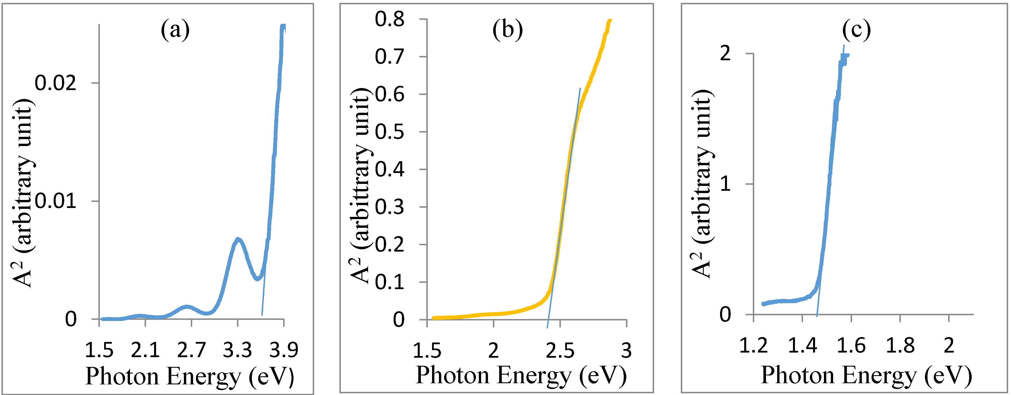
The results of optical absorption measurements for the electrodeposited ZnS, CdS and CdTe layers are presented in
Figure 2a–c, respectively. The figures show that the electrodeposited ZnS, CdS and CdTe layers have energy bandgaps of 3.70 eV, 2.42 eV and 1.45 eV, respectively. The ZnS optical response displays interference fringes as reported previously [
22] with very low absorbance compared to CdS layer for approximately equal thicknesses. This makes ZnS a suitable candidate for use as effective buffer/window layer in CdTe-based multilayer graded bandgap solar cells.
Figure 2.
Square of absorbance (A2) vs. photon energy for annealed layers of (a) ZnS, (b) CdS and (c) CdTe.
Figure 2.
Square of absorbance (A2) vs. photon energy for annealed layers of (a) ZnS, (b) CdS and (c) CdTe.
It is important to note what happens to the ZnS/CdS/CdTe structure in the annealing process. This structure was annealed at a temperature of 450 °C for 15 min in air after CdCl
2 + CdF
2 treatment. Interdiffusion of S and Te due to this annealing results in the formation of CdS
xTe
1−x intermediate material at the CdS/CdTe interface. This intermediate material is expected to have a bandgap between those of CdS and CdTe, thus causing a grading in bandgap between CdS and CdTe. Also interdiffusion of Zn and Cd between ZnS and CdS results in the formation of the intermediate material, Zn
xCd
1−xS at the ZnS/CdS interface. The overall result is a grading, closer to the hetero-junctions, in the energy bandgap of the ZnS/CdS/CdTe structure.
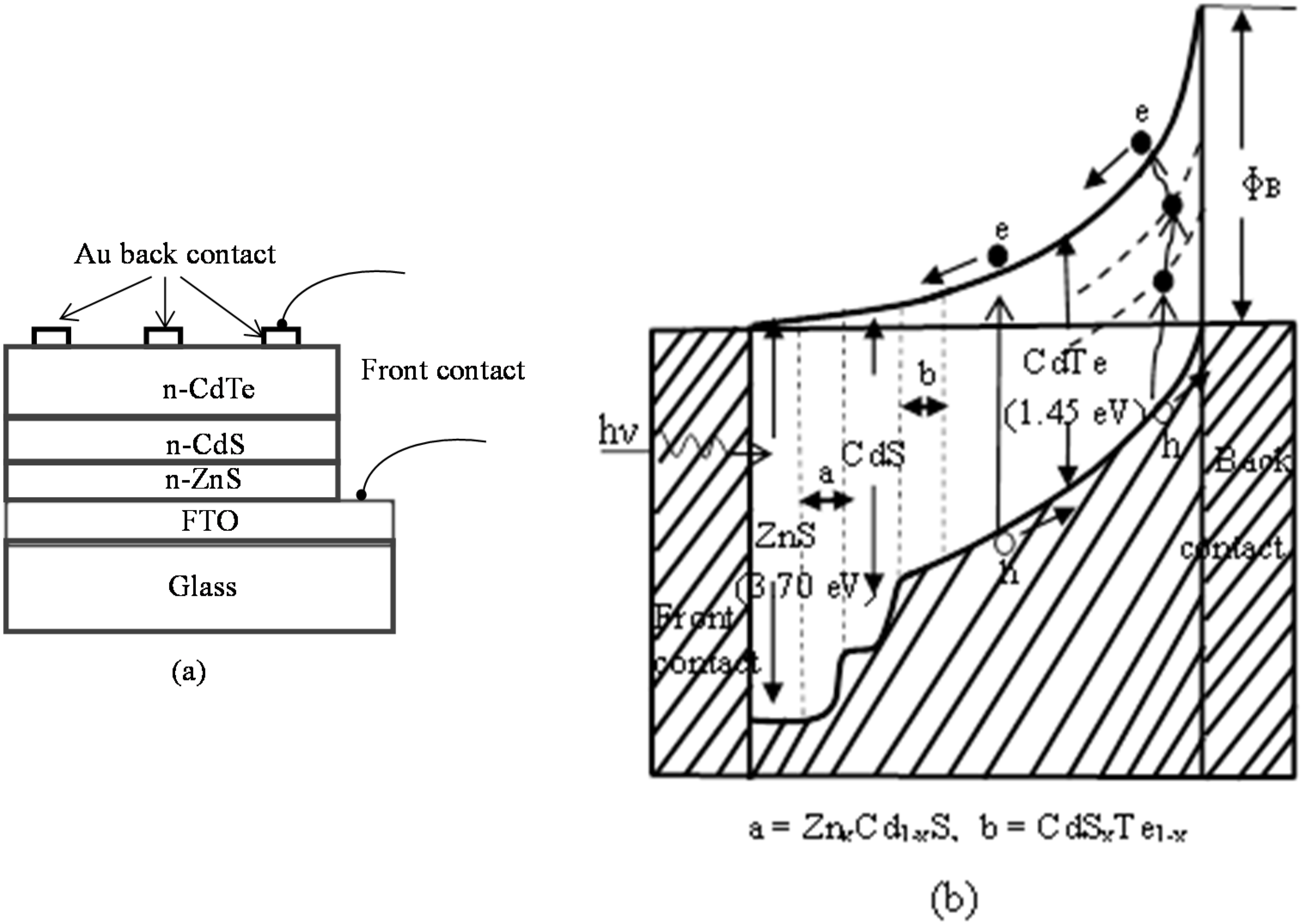
Figure 3a,b, respectively, show a schematic of the device structure and the resulting energy band diagram of the glass/FTO/n-ZnS/n-CdS/n-CdTe/Au solar cell. The large Schottky barrier height (φ
B) at the n-CdTe/metal junction creates the major required band bending (depletion region) that provides strong electric field for separation of photo-generated electron-hole pairs as soon as they are created in the device. The strong electric field and a healthy depletion region help to impose high velocity on the photo-generated charge carriers resulting in high current density. Due to the prevalent Fermi level pinning phenomenon in CdTe, these devices are processed so as to have the Fermi level pinned very close to the top of the valence band [
25,
28].
The n-n hetero-junctions at n-ZnS/n-CdS and n-CdS/n-CdTe interfaces may or may not form rectifying junctions depending on the manner in which they are formed and the degree of inter-diffusion between the elements of the two semiconductors involved in each case [
33] especially during the post-deposition heat treatment. However, the difference in the bandgaps of the materials contributes to improvement in the slope of the energy band diagram, which represents the built-in electric field. If these interfaces become rectifying eventually, the depletion regions formed rather become complementary to the main depletion region at the n-CdTe/Au interface. This gives rise to a fully depleted device with electric field throughout the entire thickness of the device for effective separation and collection of photo-generated charge carriers.
Figure 3.
(a) Schematic of the glass/FTO/n-ZnS/n-CdS/n-CdTe/Au graded bandgap device and (b) Energy band diagram of the glass/FTO/n-ZnS/n-CdS/n-CdTe/Au graded bandgap solar cell structure showing impurity PV effect through defect levels in the bandgap of CdTe (not drawn to scale).
Figure 3.
(a) Schematic of the glass/FTO/n-ZnS/n-CdS/n-CdTe/Au graded bandgap device and (b) Energy band diagram of the glass/FTO/n-ZnS/n-CdS/n-CdTe/Au graded bandgap solar cell structure showing impurity PV effect through defect levels in the bandgap of CdTe (not drawn to scale).
With this situation in place therefore, charge carriers generated in CdS and ZnS by high-energy photons are not lost but are rather collected and they therefore contribute to the photo-generated current density in the solar cell. The intermixing at the n-n hetero-interfaces in addition helps to provide a graded hetero-junction instead of an abrupt one. This in turn, helps to create a smooth potential gradient based on the difference in the energy bandgaps of the two adjacent semiconductors involved in each case, for the acceleration of photo-generated charge carriers towards the electrical contacts. As a result, this device structure is regarded as a graded bandgap structure in this work. The device is therefore capable of absorbing photons from the ultraviolet to the near infrared region of the solar spectrum, improving photo-generated carrier collection, minimising thermalisation and therefore introducing a cooling effect to the device. This is because, the shape of the band diagram helps to provide fairly continuous slope of the bandgap of the device and a wide depletion region throughout the device. All this has the advantage of enhancing the acceleration of photo-generated charge carriers towards the metal contacts for collection into an external circuit. The device therefore forms a combination of two n-n hetero-junctions and a large Schottky barrier structure with a resultant healthy depletion region. It should be noted that these graded-type Schottky barrier structures are capable of producing potential barrier heights (~1.20 eV) greater than or comparable to p-n junction devices. By constructing metal-insulator-semiconductor (MIS) type contacts, barrier heights greater than the bandgap of CdTe can be produced. The glass/FTO/n-CdS/n-CdTe/Au 2-layer solar cell is also similar to the glass/FTO/n-ZnS/n-CdS/n-CdTe/Au 3-layer counterpart in structure and is used as a control experiment in this work to compare the advantages of the graded bandgap architecture with ZnS as wide bandgap buffer/window layer.
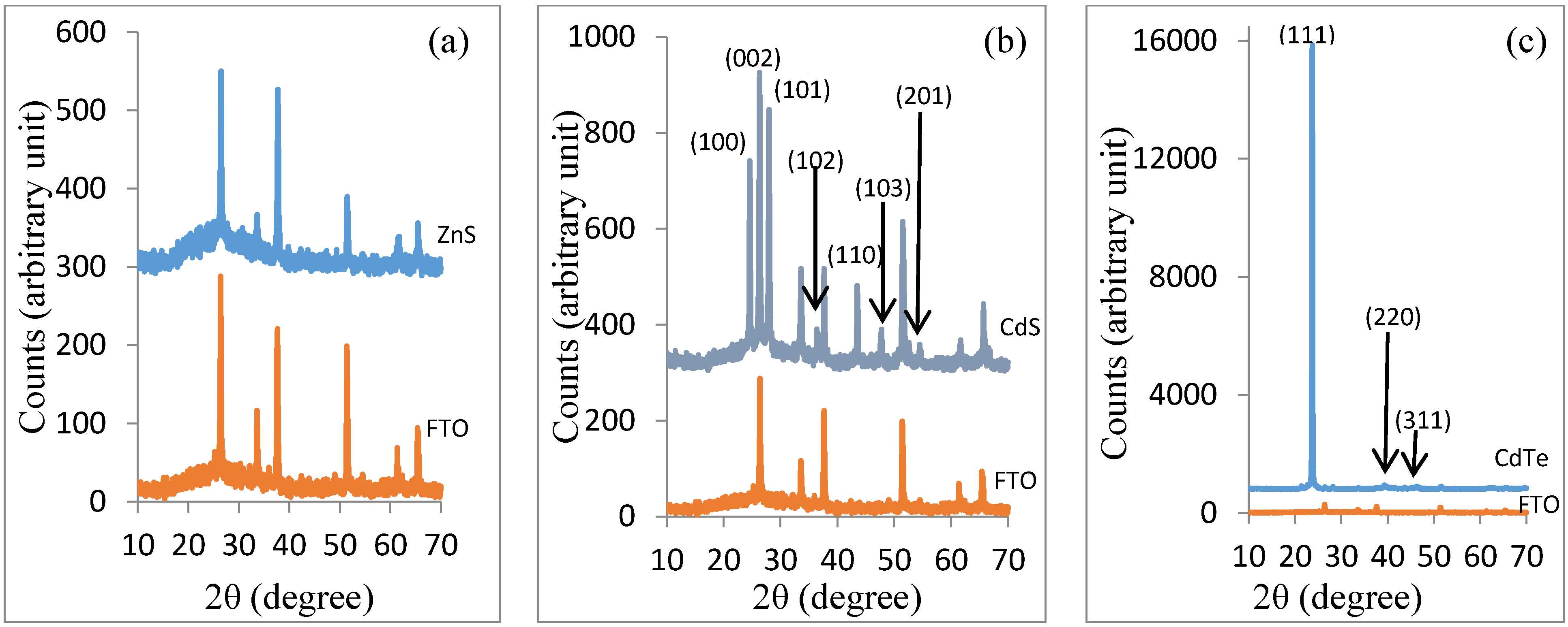
Figure 4a–c shows the X-ray diffraction patterns of the electrodeposited ZnS, CdS and CdTe thin layers, respectively. The ZnS layers were armophous and therefore did not show any relevant diffraction peaks. All the peaks present in the diffraction pattern belong to the underlying polycrystalline FTO substrate. This amorphous nature of ZnS is viewed as an advantage in the sense that it provides a more uniform coverage of the FTO substrate by ZnS without gaps between the grains so that the next layer (polycrystalline CdS) will not come into direct contact with the FTO front contact through any possible gaps between ZnS grains. This issue is an important one since the electrodeposition process is electric field-driven. In line with the laws of electrostatics, these fields will naturally tend to concentrate on sharp spikey points on the substrate and encourage preferential nucleation and columnar growth of grains, especially when compared to the case of electroless techniques. As mentioned earlier, one major problem encountered in solar cell fabrication is that of the presence of these rough and spikey surfaces on the transparent conducting oxide substrate usually used as front electrical contact. This often causes uneven coverage of this substrate by the thin window material such as CdS, leaving uncovered spikey portions of the substrate. This eventually creates shunting paths in the solar cell when CdTe is deposited on the window layer, resulting to loss of fill factor. For this reason therefore, the armophous ZnS layer, whose small grains spread out lateraly and closed-up together (as shown later in the SEM image), also acts as a buffer layer in addition to its function as a window material since it can effectively prevent CdS grains from coming into direct contact with the FTO front contact.
Figure 4.
X-ray diffraction patterns of electrodeposited (a) amorphous ZnS; (b) polycrystalline CdS and (c) highly oriented CdTe thin layers on glass/FTO substrates.
Figure 4.
X-ray diffraction patterns of electrodeposited (a) amorphous ZnS; (b) polycrystalline CdS and (c) highly oriented CdTe thin layers on glass/FTO substrates.
The electrodeposited CdS layers are polycrystalline in nature with hexagonal structure as shown in
Figure 4b. This stucture matches the reference JCPDS file no. 01-075-1545. The prefered orientation of the structure is in the <002> direction with the corresponding XRD peak at 2θ = 26.3°. However, the (002) peak was not used for estimating the crystallite size since it coincides with an FTO peak. As a result, the next higher peak which is the (101) peak at 2θ ~ 28.1° was used for this purpose. The estimated crystallite sizes using Scherrer equation were ~21 nm and 63 nm before and after annealing respectively. The d-spacing obtained for the annealed sample was 3.186 Å. The corresponding 2θ and d-spacing for the reference file are 28.2° and 3.164 Å respectively. The increase in crystallite size after annealing with CdCl
2 treatment shows the improvement of the crystalline quality of the layer by this annealing process.
Figure 4c shows that the electrodeposited CdTe is highly oriented in the <111> direction with a cubic structure. The (111) peak appears at an angle of 2θ = 23.6° and with d-spacing of 3.758 Å, matching the reference file no 00-015-0770 with 2θ = 23.8° and d = 3.742 Å. The estimated crystallite size for this layer was 55.4 nm both before and after annealing with CdCl
2 + CdF
2 treatment. The lack of crystallite size increase after annealing is suprising. However, it can be attributed to either saturation in the crystallite size due to the large thickness reached (~1.70 μm) or due to limitation of the Scherrer equation in addition to limitation of the software used for the diffraction peak analysis on the XRD system. In any case, the highly oriented (111) diffraction peak of this material is very impressive and is indicative of the structural quality of this electrodeposited semiconductor.
Figure 5a–c shows the optical absorption of glass/FTO/ZnS/CdS bi-layer, its transmittance after annealing and the transmittance of glass/FTO/CdS, respectively. The glass/FTO/ZnS/CdS structure was annealed at 400 °C for 20 min after CdCl
2 treatment. The underlying glass/FTO/ZnS was previously annealed at 350 °C for 10 min as mentioned earlier. This second annealing causes the interdifussion of Zn and Cd across the ZnS/CdS hetero-junction as was mentioned earlier.
Figure 5.
(a) Optical absorption of annealed glass/FTO/ZnS/CdS bi-layer; (b) transmittance of annealed glass/FTO/ZnS/CdS bi-layer and (c) transmittance of glass/FTO/CdS layer.
Figure 5.
(a) Optical absorption of annealed glass/FTO/ZnS/CdS bi-layer; (b) transmittance of annealed glass/FTO/ZnS/CdS bi-layer and (c) transmittance of glass/FTO/CdS layer.
A blue shift corresponding to an enhancement in the transmission of higher energy photons in the wavelength range 312–500 nm is obvious in
Figure 5b when compared with
Figure 5c. This will have the overall effect of allowing more higher energy photons into the CdTe absorber layer for creation of more charge carriers and therefore improving the photocurrent and overall performance of the resulting solar cell. Overall, the different material layers can absorb photons from different regions of the solar spectrum to create photo-generated charge carriers and these will collectively combine to improve the photocurrent produced by the solar cell. This result has been observed in the solar cell fabricated using the ZnS/CdS/CdTe structure in comparison with that using only CdS/CdTe structure, which is the main focus of this paper in addition to the succesful application of electrodeposition technique in fabricating these device structures.
Figure 6a–c shows the scanning electron micrographs of the electrodeposited ZnS, CdS and CdTe layers, respectively.
Figure 6a shows ZnS with uniform coverage of the glass/FTO substrate without any visible pinholes at the magnification of 60,000× used. This is a good sign as mentioned earlier for the growth of CdS. The estimated sizes of the grains are in the range 208–417 nm. In
Figure 6b, the nature of CdS growth is revealed. The crystallites and therefore the grains tend to grow in an upward direction perpendicular to the substrate, leaving some gaps between them [
34]. This can pose serious problems in solar cell fabrication when CdS is deposited directly on the FTO. The estimated grain sizes are in the 167–375 nm range. These observed CdS grains actually consist of groups of crystallites that agglomerated together. CdTe crystallites can go through these gaps between the grains and tend to deposit on the uncovered (exposed) portions of FTO when there is no buffer layer, since this is the path of least resistance. This in turn causes short-circuits in the device resulting mainly in loss of fill factor and low open-circuit voltage.
Figure 6.
Scanning electron micrographs of electrodeposited (a) amorphous ZnS; (b) polycrystalline CdS and (c) highly oriented CdTe thin layers.
Figure 6.
Scanning electron micrographs of electrodeposited (a) amorphous ZnS; (b) polycrystalline CdS and (c) highly oriented CdTe thin layers.
A possible way of preventing this is using a buffer layer (such as ZnS in this case) or by making the CdS crystallites and grains grow laterally and fatter instead of growing as vertically oriented rods, so that they can close up the gaps when they touch each other. Growing thick CdS layers helps to achieve this but at the same time this increases the light absorption near the surface of CdS and drastically reduces the amount of photons that reach the depletion region for creation of electron-hole pairs due to the position of the depletion region. CdTe tends to grow also in upward direction as columns. However, due to the large thickness grown compared to CdS, the grains touch each other towards the surface of the layer and tend to close up the gaps between them so that the micrograph shows no visible pinholes or gaps between the grains as shown in
Figure 6c. What is seen therefore are clusters of tightly-packed grains with these clusters of grains touching each other. The grains are also made up of tightly-packed smaller crystallites. The estimated grain sizes (or clusters) in
Figure 6c are in the 217–870 nm range.
Figure 7a,b shows the LogI
vs. V graphs under dark conditions for the glass/FTO/ZnS/CdS/CdTe/Au 3-layer graded-bandgap solar cell and glass/FTO/CdS/CdTe/Au 2-layer solar cell, respectively.
Figure 7.
LogI vs. voltage under dark conditions for (a) glass/FTO/ZnS/CdS/CdTe/Au 3-layer solar cell and (b) glass/FTO/CdS/CdTe/Au 2-layer solar cell.
Figure 7.
LogI vs. voltage under dark conditions for (a) glass/FTO/ZnS/CdS/CdTe/Au 3-layer solar cell and (b) glass/FTO/CdS/CdTe/Au 2-layer solar cell.
Each of the figures is a combination of LogI-V for both forward and reverse bias conditions. The diode parameters under dark condition (such as barrier height, ϕ
B, ideality factor,
n, rectification factor,
R.F., and reverse saturation current density,
J0) are obtained from these graphs. The Schottky barrier heights estimated for the two device structures were >1.13 eV and >1.10 eV for glass/FTO/ZnS/CdS/CdTe/Au and glass/FTO/CdS/CdTe/Au devices, respectively. These values most likely represent the average values of all the barrier junctions present in the devices. The diode ideality factors obtained were respectively 2.37 and 2.54. The large ideality factor values in excess of 2.00 indicate the possible presence of high series resistance, a contribution from tunnelling and the presence of high concentration of recombination and generation centres in the device structures and these underestimate the potential barrier heights of the devices. The diode rectification factor [
R.F. = (
IF/
IR)
V=1] of each solar cell was obtained as the ratio of the forward current,
IF, to the reverse current,
IR, at the maximum bias voltage of 1.0 V. The rectification factors obtained for the two solar cells were 10
4.4 and 10
4.1, respectively, for glass/FTO/ZnS/CdS/CdTe/Au and glass/FTO/CdS/CdTe/Au solar cells. The intercept of the straightline portion of the forward current on the LogI axis is used to calculate the reverse saturation current density of the solar cells using the cell active area of ~0.031 cm
2. The large Schottky barrier heights ϕ
B >1.10 eV and the high rectification factors,
R.F. >10
4 obtained for both solar cell structures indicate how strong the electric field in the depletion region is for effective separation of photo-generated charge carriers. This high field actually imposes high drift velocity on the photo-generated charge carriers, and due to the high quality of the electrodeposited materials (columnar nature of CdS and CdTe grains), this leads to high short-circuit current densities observed for the devices.
Table 1 summarises the device parameters of the two solar cell structures both under dark and illumination conditions. These results represent those of the best devices for each device structure among several attempts. The rest of the devices generally have efficiencies less than 8.0% and are therefore not presented here for brevity. Low efficiencies could arise due to existence of shunting paths through pinholes and detrimental defects via recombination.
Figure 8a,b also shows the linear-linear dark current density-voltage (J-V) curves for the glass/FTO/ZnS/CdS/CdTe/Au 3-layer solar cell and glass/FTO/CdS/CdTe/Au 2-layer solar cell structures, respectively. From these graphs, the dark series and shunt resistances of the devices can be obtained. The graphs also show the good diode rectifying property of the cells under dark condition as a compliment to
Figure 7. The shapes of the forward curves show that the glass/FTO/CdS/CdTe/Au 2-layer solar cell (
Figure 8b) suffers from high dark series resistance compared to the glass/FTO/ZnS/CdS/CdTe/Au 3-layer solar cell.
Figure 8.
Linear-linear dark current density-voltage graph for (a) glass/FTO/ZnS/CdS/CdTe/Au 3-layer solar cell and (b) glass/FTO/CdS/CdTe/Au 2-layer solar cell, under forward and reverse bias conditions.
Figure 8.
Linear-linear dark current density-voltage graph for (a) glass/FTO/ZnS/CdS/CdTe/Au 3-layer solar cell and (b) glass/FTO/CdS/CdTe/Au 2-layer solar cell, under forward and reverse bias conditions.
Table 1.
Summary of device parameters for the two solar cell structures for comparison.
Table 1.
Summary of device parameters for the two solar cell structures for comparison.
| Measurement Condition | Device Parameter | Glass/FTO/ZnS/CdS/CdTe/Au 3-Layer Solar Cell | Glass/FTO/CdS/CdTe/Au 2-Layer Solar Cell |
|---|
| Dark | R.F. ≈ (IF/IR)V = 1 | 104.4 | 104.1 |
| n | 2.37 | 2.54 |
| J0 (A·cm−2) | 8.0 × 10⁻⁸ | 1.0 × 10⁻⁷ |
| ϕB (eV) | >1.13 | >1.10 |
| Dark C-V | Nd-Na (cm−3) | 8.1 × 10¹⁴ | 2.5 × 10¹⁵ |
| Illuminated (AM 1.5) | Rs (Ω) | 175 | 316 |
| Rsh (Ω) | 3825 | 4574 |
| Voc (mV) | 640 | 630 |
| Jsc (mA·cm−2) | 40.8 | 38.5 |
| FF | 0.40 | 0.33 |
| η (%) | 10.4 | 8.0 |
For comparison
Figure 9a,b shows the linear-linear I-V characteristics of the best glass/FTO/ZnS/CdS/CdTe/Au 3-layer graded-bandgap solar cell and glass/FTO/CdS/CdTe/Au 2-layer solar cell under AM 1.5 illumination conditions at room temperature, respectively. The result of using ZnS as the buffer/window layer is directly reflected in the improved high short-circuit current density (
Jsc) as well as improved open-circuit voltage (
Voc), fill factor (
FF) and ultimately, the conversion efficiency (η) of the 3-layer graded-bandgap device, compared to the glass/FTO/CdS/CdTe/Au 2-layer device as shown in
Figure 9a,b. The device parameters under AM1.5 illumination conditions are also summarised in
Table 1.
The measured Voc values of 640 mV and 630 mV are not as large as expected and are indicative of the presence of leakage paths which is also evident in the low fill factor values obtained. The low Voc values can also arise due to low-purity chemicals used to deposit some semiconductors in this work.
A major weakness of these solar cells is the very low fill factor values, and their improvement is a major challenge. Again, the observed remarkable high short-circuit current densities are not consistently observed and the devices tend to degrade after few weeks and even days in some cases. This raises stability and reproducibility issues and poses great challenges to the research at present. However, to ensure that the observed high Jsc values are genuine, the diodes producing them were isolated by carefully removing the CdTe material around them and repeating the I-V measurements. The high short-circuit current remains indicating that these observations are not due to collections from the periphery of the device. Work is in progress to optimise the materials growth and device fabrication steps in order to improve the stability and reproducibility, as well as the efficiencies of these devices by improving the fill factors and the open-circuit voltages further.
Figure 9.
I-V characteristics of (a) glass/FTO/ZnS/CdS/CdTe/Au 3-layer graded bandgap solar cell and (b) glass/FTO/CdS/CdTe/Au 2-layer solar cell under AM 1.5 illumination conditions at room temperature.
Figure 9.
I-V characteristics of (a) glass/FTO/ZnS/CdS/CdTe/Au 3-layer graded bandgap solar cell and (b) glass/FTO/CdS/CdTe/Au 2-layer solar cell under AM 1.5 illumination conditions at room temperature.
It is important at this point to comment on the unusual high J
sc values observed for these devices as shown in
Table 1 and
Figure 9. To do this, we recall the existence of several native defect/impurity levels within the energy bandgap of CdTe which are known to cause Fermi level pinning phenomenon at CdTe/metal interfaces [
28,
32,
35]. Two of such impurity levels have been shown in the energy band diagram in
Figure 3b for illustration. The presence of these defect levels coupled with the position of the depletion region and the overall shape of the energy band diagram of these devices (see
Figure 3b) work together to make room for these observed high
Jsc values. It is therefore possible in these solar cells for photons with energy lower than the energy bandgap of CdTe to create useful electron-hole pairs that contribute to photo-generated current. These infrared photons which can come both from the incident solar radiation and the heat energy in the surroundings of the solar cell, can promote electrons from the valence band to the nearest impurity/defect level near the CdTe/metal junction of the device. As soon as this happens, the hole created in the valence band quickly drifts towards the Au back metal contact by the strong electric field in this region due to the existence of the depletion region in this area of the device. As a result, the electron promoted to the defect level has no room for relaxing back into the valence band to recombine with the hole. It can then be successively promoted to the conduction band by other infrared photons through the “ladder” of defect levels to contribute to photo-generated current. This is impurity photovoltaic effect taking place in PV devices with the right conditions. Alternatively, this electron can be “knocked out” from the defect level directly into the conduction band by another electron accelerating down the band structure towards the front contact, from the high Schottky barrier height (ф
B ~1.20 eV) existing at the n-CdTe/Au interface in a form of impact ionisation. In other words these two phenomena (impurity photovoltaic effect and impact ionisation) can combine in one device to give rise to high short-circuit current density as is observed in the devices presented in this paper. This is possible due to the position of the major depletion region in the device (near the n-CdTe/Au interface) and the overall shape of the band diagram of the devices. Full description of next generation solar cells based on graded bandgap devices, and the reasons for observing high current densities are reported in [
36].
These effects may not be as easy in a p-n junction-type device structure, primarily due to the position of the depletion region. In this case, electrons can equally be promoted to available defect levels near the p-CdTe/metal ohmic contact. However, due to the existence of “flat band condition” in this region (since the depletion region is at the n-CdS/p-CdTe junction), the hole created in the valence band cannot easily drift towards the back metal contact since there is no electric field in this region. As a result, both this hole and the electron promoted to the defect level are within each other’s reach for easy recombination. Also the type of impact ionisation described above (within the CdTe material) is difficult to happen in the p-n junction-type solar cell for the same reason. If however the p-n junction device is fully depleted with its depletion region extending throughout the entire thickness of the CdTe, these effects may also be observed. The design of the device structures used in the solar cells described in this paper and in [
36] are therefore of significant importance.
Although the authors have not been able to carry out measurements such as quantum efficiency (QE) and responsivity as a means of confirming the experimental evidence of impurity photovoltaic effect and impact ionisation in these solar cells, these effects have been experimentally confirmed in a recent work on GaAs/AlGaAs graded bandgap solar cells published by the authors’ group [
32,
36,
37,
38]. These publications also highlighted a major technical deficiency of QE measurement [
37]. Whereas responsivity measurements revealed the photocurrent generation by photons with energy lower than the bandgap of GaAs, QE measurements could not reveal this effect. Also a recent unpublished work on the GaAs/AlGaAs graded bandgap solar cells by the authors’ group has produced solar cells with internal photon-to-current conversion efficiency (IPCE) as high as 140% [
36], showing experimental evidence of impact ionisation. In the present work reported in this paper, the device structures have been designed to incorporate these two effects as described earlier. However, the reason for not having carried out responsivity measurements (preferably) on these devices has to do with the issue of poor stability and reproducibility of these devices at present. Once these issues are resolved, the authors anticipate carrying out these measurements in laboratories where the two techniques are available. Since this could take some time, the authors are reporting their observations on these devices at present.
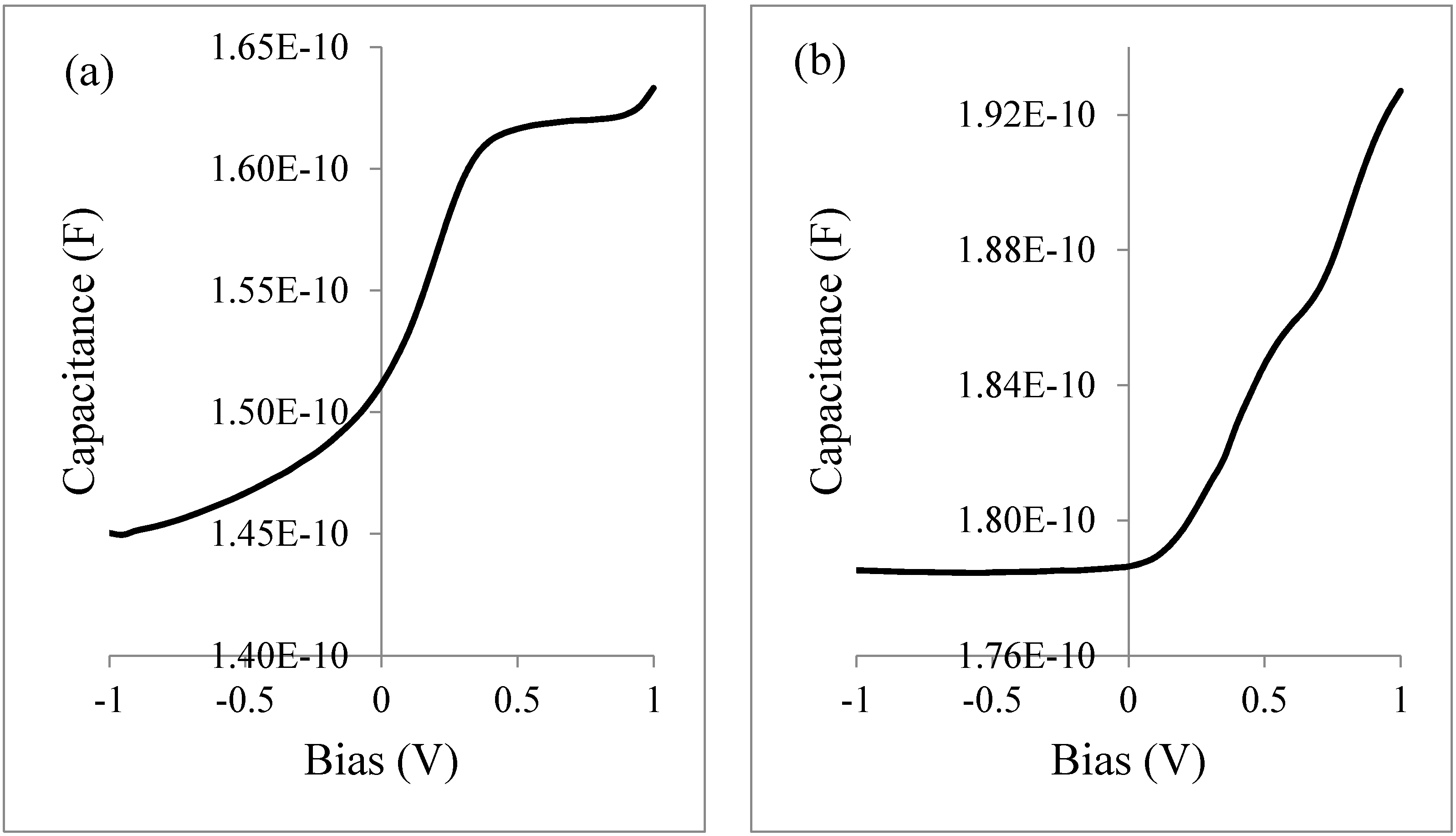
The capacitance-voltage (C-V) relationship of the glass/FTO/ZnS/CdS/CdTe/Au 3-layer and glass/FTO/CdS/CdTe/Au 2-layer devices at a frequency of 1 MHz are shown in
Figure 10a,b, respectively, and the corresponding Mott-Schottky plots of these devices are shown in
Figure 11a,b. For the glass/FTO/ZnS/CdS/CdTe/Au structure,
Figure 10a shows that the depletion capacitance gradually increases from reverse bias of −1.0 V to forward bias. The depletion capacitance measured for this device at zero applied bias was
Co~151 pF. For the glass/FTO/CdS/CdTe/Au device, the capacitance remains constant under reverse bias condition and begins to increase with forward bias as shown in
Figure 10b. The rate of increase in capacitance in the forward bias for the two devices under study in
Figure 10 is essentially the same. The depletion capacitance obtained for the glass/FTO/CdS/CdTe/Au device was
Co~179 pF. These capacitance values suggest that the glass/FTO/ZnS/CdS/CdTe/Au 3-layer graded-bandgap solar cell has a wider depletion region compared to the glass/FTO/CdS/CdTe/Au 2-layer solar cell. However,
Figure 10b shows that the 2-layer device is fully depleted even at zero bias and the depletion region width becomes smaller than the thickness of the device at forward bias. This seeming contradiction can be due to interface states especially in the case of the 3-layer device with more interfaces as well as due to the differences of doping concentrations in the absorber material layers. In addition, the unusual complex device architecture (n-n heterojunction + Schottky junction) can give rise to this situation, making the J-V and C-V characteristics deviate significantly from those of usual simple p-n junction or Schottky junction devices.
Figure 10.
Capacitance-Voltage plot at a frequency of 1 MHz for (a) glass/FTO/ZnS/CdS/CdTe/Au 3-layer device and (b) glass/FTO/CdS/CdTe/Au 2-layer device.
Figure 10.
Capacitance-Voltage plot at a frequency of 1 MHz for (a) glass/FTO/ZnS/CdS/CdTe/Au 3-layer device and (b) glass/FTO/CdS/CdTe/Au 2-layer device.
In
Figure 11a,b the Mott-Schottky plots for the two device structures are presented. Both figures display a slow response of 1/C
2 with applied reverse bias voltage. For the glass/FTO/ZnS/CdS/ CdTe/Au device in
Figure 11a, there is a more rapid drop in the value of 1/
C2 as forward bias increases from 0 V to ~0.35 V than in the reverse bias. Beyond 0.35 V forward bias, 1/
C2 remains fairly constant. The doping concentration of electrons estimated from
Figure 11a for this device structure was
Nd-
Na ~8.1 × 10
14 cm
−3. In the glass/FTO/CdS/CdTe/Au device structure in
Figure 11b, there is constant drop in 1/
C2 with forward bias and the doping concentration of electrons estimated for this device structure was
Nd-
Na ~2.5 × 10
15 cm
−3. As reported in the literature, solar cells with efficiencies greater than 10% show doping concentrations in the region of 5 × 10
14–1 × 10
15 [
32]. Our estimated values are in this region. Mott-Schottky plots are however, affected by other factors such as naturally existing insulating layers and various interface states, and therefore cannot be used to accurately estimate diffusion voltage and hence potential barrier height. More so, the complex nature of the device structures reported in this paper can result in significant deviation of the C-V and 1/
C2-V responses from those of simple structures. This may account for the observed large built-in potentials of the two devices as seen in
Figure 11 and perhaps the instability observed in the devices at present.
Figure 11.
Dark 1/C2 vs. V plots at 1 MHz for (a) glass/FTO/ZnS/CdS/CdTe/Au 3-layer device and (b) glass/FTO/CdS/CdTe/Au 2-layer device as a function of DC bias voltage.
Figure 11.
Dark 1/C2 vs. V plots at 1 MHz for (a) glass/FTO/ZnS/CdS/CdTe/Au 3-layer device and (b) glass/FTO/CdS/CdTe/Au 2-layer device as a function of DC bias voltage.


