
S-Rich CdS1−yTey Thin Films Produced by the Spray Pyrolysis Technique


Faculty of Science, Department of Physics, Al Isra University, Amman 11622, Jordan
Energies 2016, 9(4), 234; https://doi.org/10.3390/en9040234
Submission received: 12 January 2016
/
Revised: 12 March 2016
/
Accepted: 16 March 2016
/
Published: 24 March 2016
(This article belongs to the Special Issue Key Developments in Thin Film Solar Cells)
Abstract
:Understanding the properties of CdSTe ternary alloys is important because they always form at the interface between the CdS window layer and CdTe absorber layer in CdS/CdTe solar cells due to the intermixing. This interdiffusion is necessary because it improves the device performance. Experimental work has been devoted to studying Te rich p-type CdSxTe1−x alloys, but there is a lack of studies on S-rich n-type CdS1−yTey solid solutions. In this work, a review of the structure, morphology, and optical properties of the S-rich n-type CdS1−yTey thin films produced by the spray pyrolysis technique on glass substrates is presented.
1. Introduction
Commercial development of photovoltaic systems requires a technology which is efficient, reliable, and low cost. CdTe/CdS thin film solar cells satisfy all the aforementioned requirements [1]. Progress has been made in improving the efficiency of CdTe/CdS research devices, where a final recorded efficiency of 21.5% has been obtained [2] in the laboratory. Light absorption and charge separation in thin-film polycrystalline cadmium telluride (CdTe) photovoltaic (PV) solar cells largely occur in the vicinity of the CdS/CdTe interface [3]. Interdiffusion between CdS and CdTe at the interface occurs during the deposition of the CdTe layer, especially when using a high temperature deposition technique, and/or during CdCl2 heat treatment. This interdiffusion is bidirectional, but there is more sulfur diffusing into the CdTe than Te diffusing into the CdS [4]. The solid solution formed in the CdTe side of the junction is CdSxTe1−x where x refers to the concentration of S and it is Te-rich with p-type conductivity, while that formed in the CdS side of the junction is CdS1−yTey, where y refers to the concentration of Te and it is S-rich with n-type conductivity. A schematic of the superstrate CdS/CdTe thin film solar cell is illustrated in Figure 1, where the solid solutions on both sides of the CdS/CdTe heterojunction are shown.
Light reaches the CdTe absorber layer through the glass substrate, transparent conductive oxide (SnO2), and the window (CdS layer) passing through these solid solutions. The formation of the Te-rich CdSxTe1−x at the CdS/CdTe interface is important for efficient PV devices. That is, it modifies the spectral response of the solar cell [5], reduces the lattice mismatch at the CdS/CdTe junction [6] which is about 9% [7], and reduces the number of interfacial states and recombination centers [8,9]. The n-type CdS1−yTey could be beneficial to the diminishment of the carrier recombination rate around the CdS/CdTe junction by shifting the electrical junction away from the high recombination hetero-interface between the CdS and the interdiffusion layer [10], and it can reduce the CdS film thickness, which can be beneficial for window transmission, but also it can reduce the short wavelength optical transmission of the window layer resulting in a poor spectral response in this wavelength region [11,12]; this could lead to reduced performance of the solar cell. It can also result in lateral junction discontinuities, and non-uniform consumption of the CdS window layer. Another influence of alloying at the CdS/CdTe junction is that the lattice parameters will change due to the formation of CdTe1−xSx and CdS1−yTey solid solutions in the absorber and window layers.
The non-uniform consumption of CdS can be mitigated by CdCl2 heat treatment of the CdS layer prior to CdTe deposition to increase the density and size of CdS grains, to reduce grain boundary diffusion, and to sharpen the CdS optical transmission edge. Forming oxides on the CdS layer suppresses the Te interdiffusion from CdTe to the CdS film and the formation of a CdS1−yTey alloy [13]. That is, oxides reside on grain surfaces and penetrate grain boundaries.
Polycrystalline CdSxTe1−x and CdS1−yTey thin films can be produced by several methods such as: thermal evaporation [14,15,16,17,18], RF magnetron sputtering [16], brush plating [17], pulse plating [19], pulsed laser deposition [20], closed space sublimation (CSS) [21,22,23,24], metal organic chemical vapor deposition MOCVD [25], chemical bath deposition (CBD) [26], and spray pyrolysis (SP) [27,28] by first producing CdS films then annealing them in nitrogen atmosphere in the presence of tellurium vapor. This last method was used in this work to produce the S-rich CdS1−yTey thin films on glass substrates. The films were doped with indium because the CdS window layer in our solar cells was doped with indium to improve its electrical conductivity. Hence the S-rich solid solution in the solar cell contains indium.
From the above it is apparent that a complete understanding of the compositional, structural, electrical, and optical properties of the intermixed layers CdSxTe1−x (Te-rich) and CdS1−yTey (S-rich) that usually constitute the interfacial region in the CdS/CdTe solar cell is essential. Several authors [4,15,19,21,29,30,31] produced and characterized Te rich CdSxTe1−x thin films. For example, Marymathelane et al. [29] produced nanocrystalline CdSxTe1−x at different temperatures and studied their optical properties. Pal et al. [31] studied the electrical conductivity, thermoelectric and optical properties along with microstructural properties of CdSxTe1−x films. According to our knowledge there is little information about the production and characterization of S-rich CdS1−yTey thin films [21,27,28], so there is a need for extensive studies about the production, and properties of S-rich CdS1−yTey solid solutions to understand their influence on solar cell performance. The aim of this work is to review the production and properties of this material in the form of thin films when produced by the spray pyrolysis method on glass substrates.
2. Production of S-Rich CdS1−yTey Thin Films and CdS/CdTe Solar Cells
Polycrystalline indium doped cadmium sulfide (CdS:In) thin films were first deposited onto glass substrates by the spray pyrolysis technique at a substrate temperature of 490 °C using a home-made spraying system. This system consists of a sprayer, a heating system, and a carrier gas system. The sprayer and the heating systems are placed in a fume-hood which was locally made. Figure 2 shows a schematic of the whole system. The precursor solution of CdS thin films was prepared by dissolving 2.06 × 10⁻² moles of extra pure CdCl2∙H2O (Art. 2011, Merck, Darmstadt, Germany) and 2.24 × 10⁻² moles of thiourea (NH2)2CS (>97% S) in 350 mL of distilled water. Indium chloride (InCl3, Art.12,471, Merck) was used as a doping compound. Thus, 2.27 × 10⁻³ mole of InCl3 was added to 1000 mL of distilled water, and used for the doping process. For example, to get different doping ratios, different amounts of this solution could be used, where the ratio of indium ions to cadmium ions in the solution is defined as the doping ratio. Three doping ratios were used; 1.5%, 0.01%, and 0.0055%. Uniform and highly transparent CdS:In thin films with thickness in the range 250–720 nm were produced. The films were annealed in nitrogen atmosphere in the presence of elemental tellurium at T = 400 °C. Different ratios of tellurium in the films were obtained by changing the period of annealing. After the annealing process the films were found to change color as a function of Te concentration in the annealing atmosphere; yellow-red to dark red.
The CdS/CdTe devices were prepared in a superstrate configuration as shown in Figure 1. The different layers were prepared as described in [32,33,34,35], where the SnO2:F and CdS:In layers were deposited by the spray pyrolysis technique at substrate temperatures of 480 and 490 °C, respectively, and the CdTe layer was deposited by thermal evaporation at ambient temperature. The SnO2:F layer was etched by HNO3 and then annealed in nitrogen atmosphere at 400 °C, while the CdS:In layer was as deposited. The thicknesses of the subsequent layers SnO2 and CdS are about 0.2 and 0.5 μm, respectively, and that of CdTe is in the range of 1–1.5 μm. The thickness of the CdTe layer was restricted in this range because it is well-known that the optical absorption coefficient in CdTe is high enough so that nearly full absorption of light below ~800 nm should occur for thicknesses above 1 μm. The devices were heat treated with CdCl2 in methanol. Annealing was done in nitrogen atmosphere at 350 °C for 30 min using the annealing system described in [32]. The hot probe was used to check if the CdTe layer is p-type. Stainless steel was used to make the back contact of the CdS/CdTe solar cells.
3. Characterization Methods
The structure and phase of the films were explored by X-ray diffraction (XRD). The measurements were made with a PW1840 Compact X-ray diffractometer system (Philips, Eindhoven, The Netherlands) with Cu Kα (λ = 1.5405 Å) in the 2θ mode in the range 2°–60°. The morphology of the films was determined by scanning electron microscopy (SEM), and the composition was determined by energy dispersive X-ray spectroscopy (EDS). SEM observations and EDS analysis were performed with a scanning electron microscope (Inspect F 50, FEI, Hillsboro, OR, USA) which is supported by X-ray energy dispersive spectroscopy. The limited accuracy of the EDS system was reflected on the results and considerable uncertainties in the composition were found as seen in Table 1 and Table 2.
A double beam UV 1601 (PC) spectrophotometer (Shimadzu, Kyoto, Japan) was used to measure the transmittance of the films with respect to a piece of glass similar to the substrates. Transmittance was recorded at room temperature in the spectral range from 400 to 1100 nm. The PL spectra were recorded at T = −213 °C by a system which consists of a DISPLEX DE-202 He cryostat (Air Products, Allentown, PA, USA) capable of cooling down to −263 °C, where the Ar ion laser of wavelength 488 nm was used as an excitation source. The laser power for CdS1−yTey thin films was 30 mW, but for the CdS/CdTe thin film solar cells it was 20 mW. The diameter of the laser beam on the sample was about 2 mm. The PL signal was collected by a multi-channel optical spectrometer (an AVS-S2000 Fiberoptic Spectrometer, Avantes, Broomfield, CO, USA) which hosts two gratings. The first grating has a range: 640–1280 nm and the second grating has a range: 190–860 nm. The spectrometer resolution (FWHM) ranges from 0.3 to 10 nm depending on the recorded region and the grating.
4. Structure, Composition, and Morphology
The CdS-CdTe solid solutions can grow in the cubic (zinc blende) phase, the hexagonal (wurtzite) phase or the mixed (cubic and hexagonal) phase [14]. CdTe1−xSx has the crystallographic form of the zinc blende (ZB) structure with space group (F-43m), and CdS1−yTey the wurtzite (WZ) with space group (P63mc) structure. The mixed phase of the CdS-CdTe system shows a large miscibility gap that depends on temperature in which both phases (cubic and hexagonal) are present.
To determine the structure of the films, XRD diffractograms for three films with different Te content and hence different colors (Figure 3a–c) were recorded at room temperature and shown. In addition, the X-ray diffractogram of a film of pure CdS:In is shown (Figure 3d).
Figure 3a has the greatest Te content (darkest red color), and Figure 3c has the smallest Te content (lightest yellow-red color). As the Figure shows, the CdS:In film displays the mixed (cubic and hexagonal structure). The CdS1−yTey displays all reflection peaks of CdS:In present in diffractogram Figure 3d, but with a shift in the positions of all peaks towards smaller angles with the increase in Te content. This indicates that the lattice spacing d, and hence lattice parameters increase with the increase of Te content in the films. In addition, a satellite peak located at 2θ = 40.8° appeared in the diffraction patterns of films (Figure 3c) and (Figure 3b) which is related to the CdS1−yTey alloy. This result is opposite to that for the Te rich CdSxTe1−x solid solution, where d decreases with the increase in S content. This is shown by different authors such as; Pal et al. [31] who found a shift in the position of the (002) peak in the XRD diffractograms of CdSxTe1−x films from 2θ = 24.3° to 25.3° with change in composition (0.1 < x < 0.8). Birkmire et al. [5] who studied the diffusion of S in CdTe films reported a shift in the position of the C(111) peak of CdTe towards larger 2θ values and found a decrease in the lattice parameters of the CdTe/CdS cells after CdCl2 heat treatment. They attributed these changes to the formation of a CdTe1−xSx solid solution. Nakayama et al. [17], who studied sulfur diffusion within CdTe, found that the positions of CdTe peaks are slightly shifted and observed satellites. Murali et al. [19] showed that the variation of lattice spacing and lattice parameters with composition is linear and obeys Vegard’s law [16]. For another set of films, EDS was used to determine the composition. The concentrations of tellurium [Te], sulfur [S], and indium [In] in the films were obtained from the EDS reports, and used to find the molar ratio y, where y = [Te]/([S] + [Te]), and the percentage ratio of the concentration of indium to that of cadmium ([In]/[Cd])% in the films. The values of y are inserted in Table 1 besides the thickness of the films and the percentage ratio of indium to cadmium in the solution.
Figure 4 displays the scanning electron microscope observations for a CdS:In film (Figure 4a), and another two CdS1−yTey films with comparable thickness but different Te concentration (t = 720 and 620 nm with y = 4.51 × 10⁻² and 28.45 × 10⁻², respectively) (Figure 4b,c)). The three films are polycrystalline, but the difference between the morphologies of the CdS:In film and the CdS1−yTey films is apparent.
The grains of the CdS:In film are large (100–200 nm) and obvious, and the film appears to be compact and uniformly covered with material. On the other hand, the surface of the CdS1−yTey film in Figure 4b appears to consist of smaller grains and aggregates of smaller grains, while the CdS1−yTey film in Figure 4c appears with morphology close to that of the CdS:In film, but it shows larger grains with wider size distribution (135–625 nm). Both CdS1−yTey films contain pores, but the film in Figure 4c is more compact than that in Figure 4b, where the ImageJ software was used to find the circularity ratio as a measure of compactness of both CdS1−yTey films. It is found to be 0.563 for the image in Figure 4b, and 0.614 for the image in Figure 4c, indicating that the film in Figure 4c has higher Te concentration and it is thinner.
5. Transmittance, Absorbance and Optical Parameters
Figure 5 displays the transmittance T% of CdS1−yTey thin films of different composition and comparable thickness besides that of a CdS:In film, which was recorded at room temperature in the 290–1100 nm wavelength range. As the figure shows, the CdS:In film shows the highest transmittance, and T% of all CdS1−yTey films decreases with the increase of y, so the increase of Te content in the films results in the increase of the absorbance, and the decrease of transmittance. In addition, it is obvious from the figure that, with the increase of y, the absorption edge shifts towards longer wavelengths, and its sharpness decreases. That is, with the increase of Te in the films the absorption edge shifts from the absorption edge of CdS (2.5 eV) to that of CdTe (1.5 eV) [36].
Figure 6 displays the absorbance of the CdS1−yTey thin films and that of the CdS:In film. Comparing the absorbance of the films on the small wavelength side, it is noticed that the largest absorbance is that of the film of y = 8.52 × 10⁻², where it has a thickness of 465 nm, and [In]/[Cd]% of 3.84 ± 0.63, then that of the film with y = 3.49 × 10⁻², thickness 490 nm, and [In]/[Cd]% of 2.98 ± 0.20. The smallest absorbance is that of the film with y = 9.97 × 10⁻² that has a thickness of 420 nm and [In]/[Cd]% of 2.75 ± 1.88. The explanation of these results is that the increase of thickness, Te content and In content increase the absorbance. The net absorbance depends on the combined influence of these three factors. The film of largest absorbance has the largest indium content and comparable thickness with that of y = 3.49 × 10⁻², which has a smaller indium content. The film of smallest absorbance has the largest Te content, but the smallest thickness and the smallest indium content in the set. The absorption edges for the films are not sharp, but each curve contains two absorption edges. This means that two bandgaps are present in each case (the one of the hexagonal phase and that of the cubic phase). The sharpest absorption edge is that of the CdS:In film. Dense oscillations before the cutoff wavelength of CdS:In (≈514 nm for pure CdS) are observed, which are evidences on the presence of quantum dots [37]. Tailing is obvious in the bandgaps of the films, and it is not possible to find a monotonic relation between absorbance and composition due to the differences in film thickness and indium content of the films. In the following paragraphs, the bandgap energy and tailing in the bandgap will be estimated and discussed.
To determine the bandgap energy of the produced CdS1−yTey solid solution, the second derivative of the absorbance was deduced from the transmittance and displayed in Figure 7. The minima in the second derivative refer to the maxima in the absorbance and they indicate the values of the bandgap energies present in the solid solution. For comparison, a similar graph for a pure CdS:In thin film was displayed in Figure 7a. Two minima at λ = 500 and 485 nm are observed for the pure CdS:In beside a shoulder at λ = 480.5 nm. These are the same three minima observed by Nĕmec et al. [38] for CdS films prepared by chemical bath deposition, but the positions of these minima in their work are shifted towards shorter wavelengths. The shift is due to the size effect, where their films are nanocrystalline with radii in the range 2.6 to more than 10 nm.
According to Nĕmec et al. [38], these minima are in good agreement with the splitting of the valence band (A, B, C) at the centre of the Brillouin zone which is typical of the bulk CdS in hexagonal structure. This confirms that the CdS:In films under study in this work also contain the hexagonal phase, which is consistent with the XRD diffractograms. This result is expected, because the films were prepared at high substrate temperature (490 °C). By comparing the second derivative curves of CdS1−yTey thin films with that of the CdS:In thin film in Figure 7a, it is found that the films showed the hexagonal phase alone for y ≤ 8.52 × 10⁻², and a mixed (cubic and hexagonal phase for 9.97 × 10⁻² ≤ y ≤ 28.45 × 10⁻²). Hence two bandgaps were deduced from the second derivative curves; one for the hexagonal and the other for the cubic phase. The positions of the minima deduced from Figure 7 and the estimated values of the optical bandgap energies are inserted in Table 2, besides the values of film thickness for the whole set of films. From the table it can be noticed that the hexagonal bandgap decrease with increasing y from 2.48 eV for y = 0 (pure CdS:In) to a minimum of 2.443 eV at y = 9.97 × 10⁻² then increases with y and reaches 2.528 eV at y = 28.45 × 10⁻². Also from the Table it can be noticed that the cubic bandgap energy increases with y from 2.259 eV at y = 9.97 × 10⁻² to 2.331 eV at y = 28.45 × 10⁻², so graded bandgaps are obtained by varying the composition of the CdS1−yTey solid solution, in a way similar to the intermixing at the CdS/CdTe junction, which results with a graded region in which the bandgap depends on composition.
The explanation of these results is complicated, because the values of y obtained by the EDS analysis are not trustworthy, and because of the differences in indium content of the films. The effect of increasing indium content is to increase the bandgap, or in other words, to shift the minima to lower wavelengths, but qualitatively these results have a trend that is consistent with the model used by Ohata et al. [30] and Pal et al. [31], which they obtained for the bandgap of the Te-rich CdSxTe1−x alloy. In this model, the bandgap of the alloy can be predicted using a simple quadratic equation:
Hence the bandgap of the S-rich CdS1−yTey alloy will be given by:
where is the bowing parameter and its theoretical value is 2 [31].
Several experimental results are consistent with Equation (1) for CdSxTe1−x [16,19,39], but according to our knowledge, there are no experimental or theoretical results for CdS1−yTey. For CdSxTe1−x alloy, Duenow et al. [16] found that the bandgap decreases below the CdTe bandgap value of Eg(CdTe) = 1.5 eV, to as low as 1.41 eV at x ≅0.3, before increasing at higher x values. Ohata et al. [39] have shown that the bandgap of CdSxTe1-x alloy decreases with addition of S in the Te-rich region for values of x up to 0.25. In addition, Murali et al. [19] observed that the bandgap shifts towards CdS side as the concentration of CdS in the films increases, and got a bandgap that varies from 1.44 to 2.41 eV as the percentage of CdS increased. On the other hand, for CdSxTe1−x nanocrystalline thin films, Marymathelane et al. [29] got Eg values in the range of 1.54–2.32 eV for films of different composition and observed that the bandgap shifts towards CdS side as the concentration of CdS in the films increases, which may mean that they did not got quadratic relation between Eg and x.
In the low photon energy range it is assumed that the spectral dependence of the absorption edge follows the empirical Urbach rule given by [40,41]:
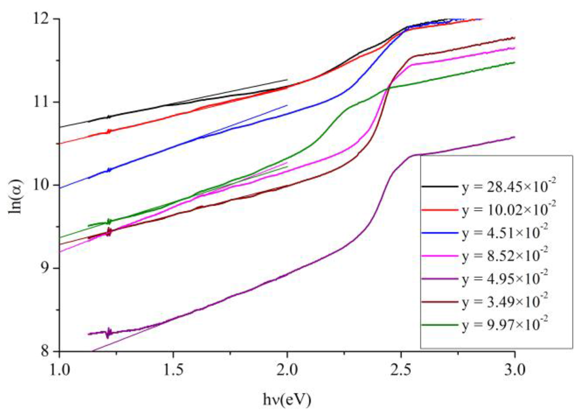
where α0 is a constant, Ee denotes an energy which is constant or weakly dependent on temperature and is often interpreted as the width of the tail of localized states in the bandgap. Therefore, to investigate this tailing, the absorption coefficient α was estimated from the transmittance measurements for the whole set of films, and the relation between the natural logarithm of the absorption coefficient ln(α) and photon’s energy hν was plotted and shown in Figure 8. A linear fit was performed in the low energy region, from which the values of Ee were estimated for all values of y and the results are inserted in Table 2. As the Table shows the values of Ee are large. The explanation of this is that low Te concentrations are known to create midgap levels in CdS [4]. In studying photoconductive lifetime of CdS used in thin film solar cells, Ahrenkiel et al. [7] found that the amplitude of the photoconductive signal is reduced by about an order of magnitude for Te doped CdS in comparison to pure CdS and the initial lifetime of the Te doped CdS is shorter than that of the pure CdS. They explained this result by saying that the effect of Te is to trap holes and act as either deep traps or recombination centers. This interpretation supports the results of this work in that it is a main reason for the large values of Ee. We did not find in the literature experimental or theoretical values of Ee for CdS1−yTey or CdSxTe1−x to compare these results with them. So these results will be used as a reference. Pal et al. [31] plotted ln(α) against photon’s energy from which they estimated the bandgap of the alloy, but they did not discuss tailing in the bandgap. By comparing Figure 8 with their graph, it is noticed that they have sharper band edges. This confirms that they have just one bandgap and hence one phase for each value of x.
α(ν) = α0 exp(hν/Ee)
Reflectance is related with transmittance by the relation T + R =1. The reflectance was deduced from the transmittance data, and used to find the refractive index n and the extinction coefficient k by using the following relation [18]:
where this definition is for the reflectance of a film for a light wave incident normally from air, with refractive index , on a medium of complex refractive index . Knowing the value of the absorption coefficient which can be deduced from the transmittance, the extinction coefficient can be calculated using the relation:
where is the wavelength in free space. Solving Equation (4) for the refractive index n gives:
The extinction coefficient k calculated from Equation (5) is plotted against the photon’s energy and displayed in Figure 9. The non-zero value of k in the region before 2.5 eV (the fundamental absorption edge of CdS) can be interpreted by the extra absorption of light that occurs at the grain boundaries, where this is known for polycrystalline films [42]. In this region k is restricted in the range 0.042–0.174, where it increases with y. A sharp increase in k occurs at the absorption edges which vary in sharpness according to y. The films with y = 9.97 × 10⁻² and y = 10.02 × 10⁻² show two absorption edges. These are due to the presence of a mixed phase in the films (cubic and hexagonal), where the cubic phase has a slightly smaller optical bandgap. After the sharp increase, k becomes constant and equal to 0.291 for all CdS1−yTey films, but for the CdS:In film it slowly decreases with hν from 0.487 to 0.453 for the energy change from 2.5 to 3.0 eV.
The refractive index n is calculated from Equation (6) and plotted against the photon’s energy and displayed in Figure 10. It is observed that n increases slowly with until the absorption edge, which is y dependent. After this, it strongly increases with , and then reaches approximately a constant value—not shown in the figure. It is obvious that the sharpest absorption edge is that of the CdS:In thin film, then sharpness decreases with y. The shift of the absorption edge towards the side of lower energy is also observed. As the figure shows, for energies before ≈2.25 eV (the fundamental absorption edge), the refractive index increases slowly with y, and its value in this region at hν = 1.5 eV—which corresponds to the bandgap energy of CdTe—lies in the range 2.10 for as-deposited CdS:In to 7.17 for the film of y = 10.02 × 10⁻².
For energies below the absorption edge, refractive index dispersion can be analyzed by the single oscillator model, so the obtained refractive index n data is also analyzed to yield the long wavelength refractive index (n∞) together with the average oscillator wavelength (λ0) for CdS1−yTey thin films of comparable thickness using the following relation [42]:
The relation between and is shown in Figure 11, beside the linear fits for the long wavelength side, where, and are evaluated from the fit parameters and listed in Table 3. From these values, the average excitation energy for electronic transitions , and the dispersion energy which is a measure of the strength of interband optical transitions , moments of the optical spectrum and are also calculated and listed in Table 3 too, where , and . From Table 3 it is observed that , , , and increase with the Te content of the films represented by (y).
The complex dielectric constant ( is the orientation sum of the dielectric constant and the loss factor components with unity dimensions. The dielectric constants of the films have been evaluated from the following equations:
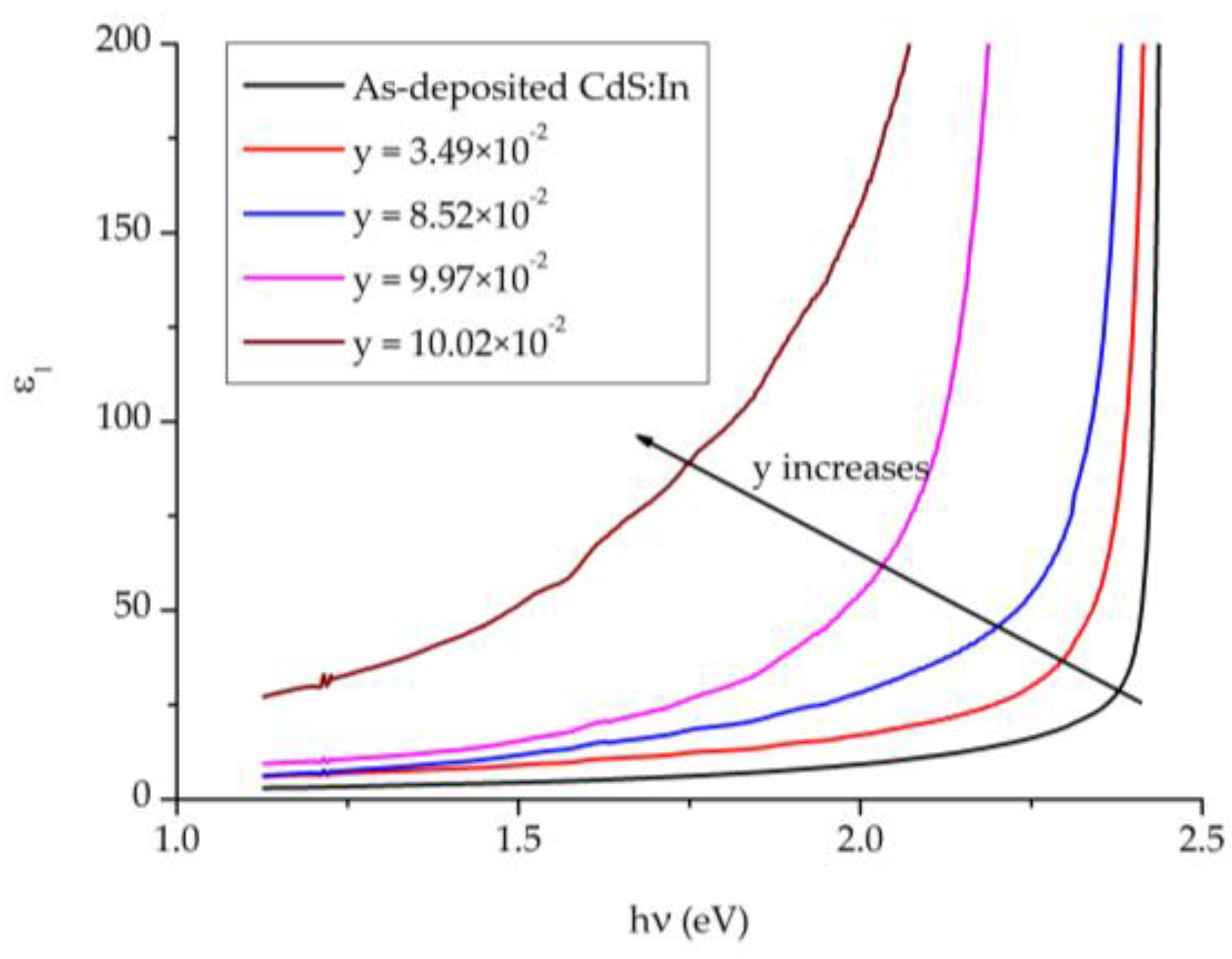
Figure 12 displays the real part of the dielectric constant ε1 against the photon’s energy for CdS1−yTey films with comparable thickness but different composition y and a CdS:In film. In the region before 1.5 eV ε1 increases with y, where it varies at hν = 1.15 eV from 2.99–28.21. It increases gradually with photons’ energy until the absorption edge, where it increases sharply. The absorption edge moves towards lower energy with the increase in y. These observations are consistent with the behavior of the extinction coefficient k and have the same explanations.
Figure 13 displays the imaginary part of the dielectric constant ε2 against the photon’s energy . In the low energy side at it increases with y and varies in the range 0.127–1.913, and it increases slowly with photon’s energy. In the region of the absorption edge, ε2 increases sharply with photon's energy, where the rate of increase decreases with y. The presence of the two phases of the CdS1−yTey solid solution causes the decrease in the rate of increase of ε2. In the high energy side after the fundamental absorption edge of CdS:In (2.5 eV), ε2 becomes constant in consistence with the behavior of the refractive index n. Both the real and imaginary parts of the dielectric constant show similar behaviors, but the imaginary part shows smaller values.
6. Photoluminescence
Figure 14 displays the photoluminescence (PL) spectra of the three CdS1−yTey thin films of diffractogramms shown in Figure 3. The PL signal was measured at −213 °C and recorded by two gratings of different ranges (the first grating has a range: 640–1280 nm and the second grating has a range: 190–860 nm). From the figure it is noticed that, in the high energy part (Figure 14a), the weakest PL signal is that of film (a) and the strongest one is that of film (c). In the low energy part (Figure 14b) the opposite is found; that is the strongest PL signal is that of film (a) and the weakest is that of film (c). The reason is that film (a) has the largest Te content and film (c) has the smallest Te content – not measured but known from annealing time in Te and color of the film. This means that as the concentration of Te increases, the shift of the PL spectra becomes deeper into the lower energy side, which is a result of the alloying of the CdS with Te. Peak-broadening observed in all PL spectra in Figure 14 is due to the superposition of spectra corresponding to the range of crystallites’ sizes present in the alloyed layer. Since the films contain particles of different sizes as seen in the SEM micrographs shown in Figure 4.
Figure 15 displays the PL spectra of the interfacial region of the CdS/CdTe solar cells—from the glass side—after CdCl2 heat treatment [43], where there is no luminescence from the CdTe side. The Figure shows the PL spectra for two solar cells with similar SnO2:F and CdS:In thickness (200 nm and 500 nm, respectively), but different CdTe layer thickness. The PL spectra in Figure 15(a) were recorded by the second grating, and that in Figure 15b were recorded by the first one. The thickness of the CdTe layer is 1.0 μm in one solar cell, and 1.5 μm in the other. It is obvious that these curves are identical to a large extent to the PL spectra of the CdS1−yTey thin films shown in Figure 14. These results confirm that these PL spectra are from the CdS1−yTey solid solution in the interfacial region of the solar cell, since as mentioned before the CdTe layer which was produced by thermal evaporation has no luminescence. The same observations found in Figure 14 are present in Figure 15. That is, first, the PL spectrum of the thicker cell has a deeper shift to the lower energy side. Second, the broadest spectrum (largest bandwidth) is that of the thicker cell. The main peaks in the solar cells’ spectra are far from the bandgap energy of CdTe (1.5 eV), but closer to the bandgap energy of CdS:In (2.5 eV), especially those of the thinner cell.
7. Conclusions
S-rich CdS1−yTey thin films were prepared by the spray pyrolysis technique. XRD diffractograms show that the films are polycrystalline, with mixed preferentially hexagonal phase. The comparison of the pure CdS:In diffractogram with those of films annealed in the presence of tellurium vapor, revealed that solid solution CdS1−yTey was formed. Transmittance and absorbance curves showed that more than one bandgap is found in each case. The second derivative curves of the absorbance were used to find the values of the optical bandgap energies. The estimated values vary according to Te concentration in the films and they covered the range 1.816–2.43 eV. The optical parameters; absorption coefficient, Urbach tail, refractive index, extiction coefficient, real and imaginary parts of the dielectric constant were all calculated and their dependence on Te concentration in the films was discussed. The dispersion parameters were estimated using the single oscillator model and their variation with Te concentration was discussed too. Photoluminescence spectra were measured at −213 °C and showed broad PL spectra. Shift of the PL spectrum towards lower energy side with Te concentration in the films was observed. These PL spectra are similar to a large extent to those of the interfacial region of CdS/CdTe solar cells, which confirms the presence of the CdS1−yTey solid solution in this region.
References
- Potter, M.D.G.; Cousins, M.; Durose, K.; Halliday, D.P. Effect of interdiffusion and impurities on thin film CdTe/CdS photovoltaic junctions. J. Mater. Sci. Mater. Electron. 2000, 11, 525–530. [Google Scholar] [CrossRef] [Green Version]
- Osborne, M. First Solar Pushes Verified CdTe Cell Efficiency to Record 21.5%. Available online: http://www.pv-tech.org/news/first_solar_pushes_verified_cdte_cell_efficiency_to_record_21.5 (accessed on 5 February 2015).
- Kuciauskas, D.; Kanevce, A.; Duenow, J.N.; Dippo, P.; Young, M.; Li, J.V.; Levi, D.H.; Gessert, T.A. Spectrally and time resolved photoluminescence analysis of the CdS/CdTe interface in thin-film photovoltaic solar cells. Appl. Phys. Lett. 2013, 102. [Google Scholar] [CrossRef]
- Dhere, R.; Rose, D.; Albin, D.; Asher, S.; Al-Jassim, M.; Cheong, H.; Swartzlander, A.; Moutinho, H.; Coutts, T.; Sheldon, P. Influence of CdS/CdTe interface properties on the device properties. In Proceedings of the 26th IEEE Photovoltaic Specialists Conference, Anaheim, CA, USA, 29 September–3 October 1997.
- Birkmire, R.W.; McCandless, B.E.; Hegedus, S.S. Effects of Processing on CdTe/CdS Materials and Devices. Int. J. Sol. Energy 1992, 12, 145–154. [Google Scholar] [CrossRef]
- Edwards, P.R. Beam-Induced Current Studies of CdTe/CdS Solar Cells. Ph.D. Thesis, University of Durham: Durham, UK, 1998. [Google Scholar]
- Ahrenkiel, R.K.; Levi, D.H.; Johnston, S.; Song, W.; Mao, D.; Fischer, A. Photoconductive lifetime of CdS used in thin-film solar cells. In Proceedings of the 26th IEEE Photovoltaic Specialists conference, Anaheim, CA, USA, 29 September–3 October 1997.
- Li, K.; Wee, A.T.S.; Lin, J.Y.; Tan, K.L. Several Efficiency Influencing Factors in CdTe/CdS Solar Cells. MRS Proc. 1997, 485. [Google Scholar] [CrossRef]
- Oman, D.M.; Dugan, K.M.; Killian, J.L.; Ceekala, V.; Ferekides, C.S.; Morel, D.L. Reduction of recombination current in CdTe/CdS solar cells. Appl. Phys. Lett. 1995, 67, 1896–1898. [Google Scholar] [CrossRef]
- Huang, C.-H.; Chuang, W.-J. Dependence of performance parameters of CdTe solar cells on semiconductor properties studied by using SCAPS-1D. Vacuum 2015, 118, 32–37. [Google Scholar] [CrossRef]
- Ngoupo, A.T.; Ouédraogo, S.; Zougmoré, F.; Ndjaka, J.M.B. New architecture towards ultrathin CdTe solar cells for high conversion efficiency. Int. J. Photoenergy 2015. [Google Scholar] [CrossRef]
- Clemminck, I.; Burgelman, M.; Casteleyn, M.; Poorter, J.D.; Vervaet, A. Interdiffusion of CdS and CdTe in screenprinted and sintered CdS-CdTe solar cells. In Proceedings of the Conference Record of the Twenty Second IEEE Photovoltaic Specialists Conference, Las Vegas, NV, USA, 7–11 October 1991; pp. 1114–1119.
- Wu, X. High-efficiency polycrystalline CdTe thin-film solar cells. Sol. Energy 2004, 77, 803–814. [Google Scholar] [CrossRef]
- Gordillo, G.; Rojas, F.; Calderón, C. Optical characterization of Cd(Sx, Te1−x) thin films deposited by evaporation. Superf. Vasio 2003, 16, 30–33. [Google Scholar]
- Kale, M.; Bhavsar, D. Synthesis and characterization of nanostructured (CdS)0.8Te0.2 thin films for solar cell application. IJESRT 2014, 3, 7012–7015. [Google Scholar]
- Duenow, J.N.; Dhere, R.G.; Moutinho, H.R.; To, B.; Pankow, J.W.; Kuciauskas, D.; Gessert, T.A. CdSxTe1−x alloying in CdS/CdTe solar cells. In Proceedings of the 2011 Materials Research Society Spring Meeting, San Francisco, CA, USA, 25–29 April 2011.
- Nakayama, N.; Arita, T.; Aramoto, T.; Nishio, T.; Higuchi, H.; Omura, K.; Ueno, N.; Murozono, M.; Takakura, H.; Omura, K.; Ueno, N.; Murozono, M.; Takakura, H. Junction structure and physical properties of heteroepitaxial CdS/CdTe. Sol. Energy Mater. Sol. Cells 1994, 35, 271–278. [Google Scholar] [CrossRef]
- Babkair, S.S.; Al-Twarqi, N.M.; Ansari, A.A. Optical characterization of CdTe films for solar cell applications. Karachi Univ. J. Sci. 2011, 39, 1–5. [Google Scholar]
- Murali, K.R.; Thirumoorthy, P.; Kannan, C.; Sengodan, V. Pulse plated CdSxTe1−x films and their properties. Sol. Energy 2009, 83, 14–20. [Google Scholar] [CrossRef]
- Compaan, A.D.; Bohn, R.G. High-Efficiency Thin-Film Cadmium Telluride Photovoltaic Cells; Final Technical Report; Contract No. ZAX-4-14013-4; National Renewable Energy Laboratory: Golden, Colorado, USA, November 1998. [Google Scholar]
- Kale, M.S.; Toda, Y.R.; Bhavsar, D.S. Synthesis and characterization of nanocrystalline (CdS)0.6Te0.4 thin films deposited by closed space sublimation technique. IOSR J. Appl. Phys. 2014, 6, 22–27. [Google Scholar] [CrossRef]
- Jácome, C.; Flórez, M.; Gurevich, Y.G.; Giraldo, J.; Gordillo, G. Characterization of CdSxTe1−x thin films through thermoelectric power measurements. J. Phys. D Appl. Phys. 2001, 34, 1862–1867. [Google Scholar] [CrossRef]
- Kosyachenko, L.; Lashkarev, G.; Grushko, E.; Ievtushenko, A.; Sklyarchuk, V.; Mathew, X.; Paulson, P.D. Spectral distribution of photoelectric efficiency of thin-film CdS/CdTe heterostructure. Acta Phys. Pol. A 2009, 116, 862–864. [Google Scholar] [CrossRef]
- Narayanswamy, C.; Gessert, T.A.; Asher, S.E. Analysis of Cu diffusion in ZnTe-based contacts for thin-film CdS/CdTe solar cells. In Proceedings of the 15th Conference NCPV Photovoltaics Program Review, Denver, CO, USA, 9–11 September 1998; pp. 9–11.
- Proskuryakov, Y.Y.; Durose, K.; Al Turkestani, M.K.; Mora-Sero, I.; Garcia-Belmonte, G.; Santiago, F.F.; Bisquert, J.; Barrioz, V.; Lamb, D.; Irvine, S.J.C.; et al. Impedance spectroscopy of thin-film CdTe/CdS solar cells under varied illumination. J. Appl. Phys. 2009, 106. [Google Scholar] [CrossRef]
- Oladeji, I.O.; Chow, L.; Liu, J.R.; Chu, W.K.; Bustamante, A.N.P.; Fredricksen, C.; Schulte, A.F. Comparative study of CdS thin films deposited by single, continuous, and multiple dip chemical processes. Thin Solid Films 2000, 359, 154–159. [Google Scholar] [CrossRef]
- Ikhmayies, S.J.; Ahmad-Bitar, R.N. CdS1−yTey thin films: Production and bandgap investigation. Sol. Energy 2012, 86, 2613–2619. [Google Scholar] [CrossRef]
- Ikhmayies, S.J.; Ahmad-Bitar, R.N. Photoluminescence and transmittance of CdS1−xTex thin films. J. Luminousc. 2012, 132, 2826–2831. [Google Scholar] [CrossRef]
- Marymathelane, R.; Ritajohn; Murali, K.R. Optical properties of CdSxTe1−X nanocrystalline thin films. Int. J. Eng. Sci. 2013, 2, 14–18. [Google Scholar]
- Ohata, K.; Saraie, J.; Tanaka, T. Optical energy gap of the mixed crystal CdSxTe1−x. Jpn. J. Appl. Phys. 1973, 12. [Google Scholar] [CrossRef]
- Pal, R.; Dutta, J.; Chaudhri, S.; Pal, A.K. CdSxTe1−x films: Preparation and properties. J. Phys. Appl. Phys. 1993, 26, 704–710. [Google Scholar] [CrossRef]
- Ikhmayies, S.J. Production and Characterization of CdS/CdTe Thin Film Photovoltaic Solar Cells of Potential Industrial Use. Ph.D. Thesis, University of Jordan: Amman, Jordan, 2002. [Google Scholar]
- Ikhmayies, S.J.; Ahmad-Bitar, R.N. The effects of post-treatments on the photovoltaic properties of spray-deposited SnO2:F thin films. Appl. Surf. Sci. 2008, 255, 2627–2631. [Google Scholar] [CrossRef]
- Ikhmayies, S.J.; Ahmad-Bitar, R.N. Effects of processing on the electrical and structural properties of spray deposited CdS:In thin films. Physica B 2009, 404, 2419–2424. [Google Scholar] [CrossRef]
- Ikhmayies, S.J.; Ahmad-Bitar, R.N. Characterization of vacuum evaporated CdTe thin films prepared at ambient temperature. Mater. Sci. Semicond. Process. 2013, 16, 118–125. [Google Scholar] [CrossRef]
- Ikhmayies, S.J. Optical parameters of CdS1−xTex thin films. In Characterization of Minerals, Metals, and Materials, Proceedings of the Characterization of Metals, Minerals and Materials, Orlando, FL, USA, 15–19 March 2015; pp. 409–416.
- Ikhmayies, S.J.; Ahmad-Bitar, R.N. Optical properties of nanocrystalline CdTe thin films. Physica B 2010, 405, 3141–3144. [Google Scholar] [CrossRef]
- Nĕmec, P.; Nĕmec, I.; Nahálková, P.; Knížek, K.; Malý, P. Ammonia-free chemical bath deposition of CdS films: Tailoring the nanocrystal sizes. J. Cryst. Growth 2002, 240, 484–488. [Google Scholar] [CrossRef]
- Ohata, K.; Saraie, J.; Tanaka, T. Phase diagram of the CdS-CdTe pseudobinary system. Jpn. J. Appl. Phys. 1973, 12, 1198–1204. [Google Scholar] [CrossRef]
- Bilgin, V.; Kose, S.; Atay, F.; Akyuz, I. The effect of substrate temperature on the structural and some physical properties of ultrasonically sprayed CdS films. Mater. Chem. Phys. 2005, 94, 103–108. [Google Scholar] [CrossRef]
- Natsume, Y.; Sakata, H.; Hirayama, T. Low temperature electrical conductivity and optical absorption edge of ZnO films prepared by chemical vapor deposition. Phys. Stat. Sol. 1995, 148, 485–495. [Google Scholar] [CrossRef]
- Tüzemen, E.Ş.; Eker, S.; Kavak, H.; Esen, R. Dependence of film thickness on the structural and optical properties of ZnO thin films. App. Surf. Sci. 2009, 255, 6195–6200. [Google Scholar] [CrossRef]
- Ikhmayies, S.J.; Ahmad-Bitar, R.N. Interface photoluminescence of the SnO2:F/CdS:In/CdTe thin film solar cells prepared partially by the spray pyrolysis technique. J. Luminous. 2012, 132, 502–506. [Google Scholar] [CrossRef]
Figure 1.
A schematic of the superstrate configuration of the SnO2/CdS/CdTe thin film solar cell, where the solid solutions on both sides are shown (drawing is not to scale).
Figure 1.
A schematic of the superstrate configuration of the SnO2/CdS/CdTe thin film solar cell, where the solid solutions on both sides are shown (drawing is not to scale).

Figure 2.
A schematic of the home-made spraying system. 1. Electrical Heater; 2. Copper Plate; 3. Aluminum Plate; 4. Substrates; 5. Insulation; 6. Spraying Nozzle; 7. Bulb of PVC; 8. Temperature Controller; 9. Stopcocks; 10. Solution; 11. Glass Dewar; 12. Cover; 13. Rubber Tubes; 14. T-Connector; 15. Fan; 16. Regulator; 17. Nitrogen Cylinder; 18. Thermocouple; 19. Fume-Hood; 20. Stand.

Figure 3.
X-ray diffractograms of three CdS1−yTey films (a–c) with different Te content besides the diffractogram of as-depoited CdS:In film (d); Film (a) has the greatest Te content and film (c) has the smallest.
Figure 3.
X-ray diffractograms of three CdS1−yTey films (a–c) with different Te content besides the diffractogram of as-depoited CdS:In film (d); Film (a) has the greatest Te content and film (c) has the smallest.

Figure 4.
SEM images of a CdS:In thin film (a) [36], and two CdS1−yTey films with comparable thickness and different values of y; (b) y = 4.51 × 10⁻², t = 720 nm; (c) y = 28.45 × 10⁻², t = 620 nm. Note: The scale in (a) is 1 μm, and the scales in (b,c) are both 500 nm.
Figure 4.
SEM images of a CdS:In thin film (a) [36], and two CdS1−yTey films with comparable thickness and different values of y; (b) y = 4.51 × 10⁻², t = 720 nm; (c) y = 28.45 × 10⁻², t = 620 nm. Note: The scale in (a) is 1 μm, and the scales in (b,c) are both 500 nm.

Figure 5.
Transmittance of CdS1−yTey thin films of different composition and comparable thickness beside that of a CdS:In film.
Figure 5.
Transmittance of CdS1−yTey thin films of different composition and comparable thickness beside that of a CdS:In film.

Figure 6.
The absorbance of CdS1−yTey thin films of different composition and comparable thickness besides that of a CdS:In film.
Figure 6.
The absorbance of CdS1−yTey thin films of different composition and comparable thickness besides that of a CdS:In film.

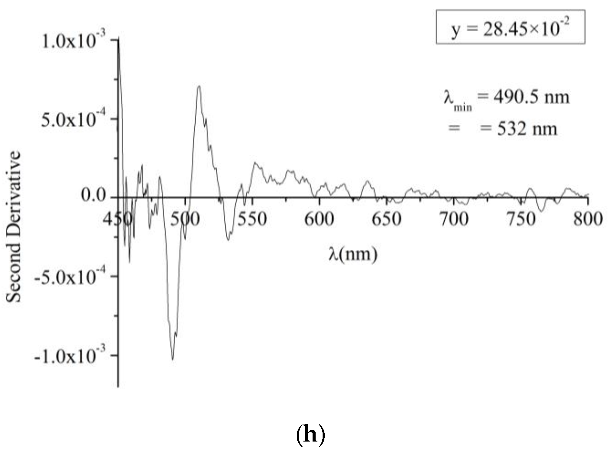
Figure 7.
The second derivative of the absorbance against the wavelength of incident radiation for (a) a CdS:In film; and (b–h) CdS1−yTey thin films of different composition.
Figure 7.
The second derivative of the absorbance against the wavelength of incident radiation for (a) a CdS:In film; and (b–h) CdS1−yTey thin films of different composition.


Figure 8.
The relation between ln(α) and hν for CdS1−yTey thin films with the linear fits.

Figure 9.
The extinction coefficient k of a CdS:In film and the CdS1−yTey thin films with comparable thickness and different composition y.
Figure 9.
The extinction coefficient k of a CdS:In film and the CdS1−yTey thin films with comparable thickness and different composition y.

Figure 10.
The refractive index of a CdS:In film and CdS1−yTey thin films of comparable thickness with different composition y.
Figure 10.
The refractive index of a CdS:In film and CdS1−yTey thin films of comparable thickness with different composition y.

Figure 11.
The plot of against for a CdS:In film and CdS1−yTey thin films of different composition y but comparable thickness.
Figure 11.
The plot of against for a CdS:In film and CdS1−yTey thin films of different composition y but comparable thickness.

Figure 12.
The real part of the dielectric constant of CdS1−yTey thin films of comparable thickness but different composition besides that of a CdS:In thin film.
Figure 12.
The real part of the dielectric constant of CdS1−yTey thin films of comparable thickness but different composition besides that of a CdS:In thin film.

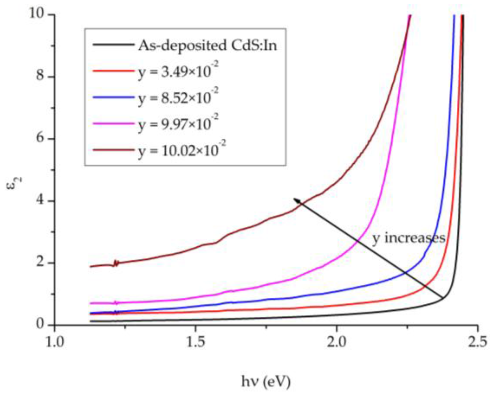
Figure 13.
The imaginary part of the dielectric constant of a CdS:In thin film and CdS1−yTey thin films of different composition but comparable thickness.
Figure 13.
The imaginary part of the dielectric constant of a CdS:In thin film and CdS1−yTey thin films of different composition but comparable thickness.

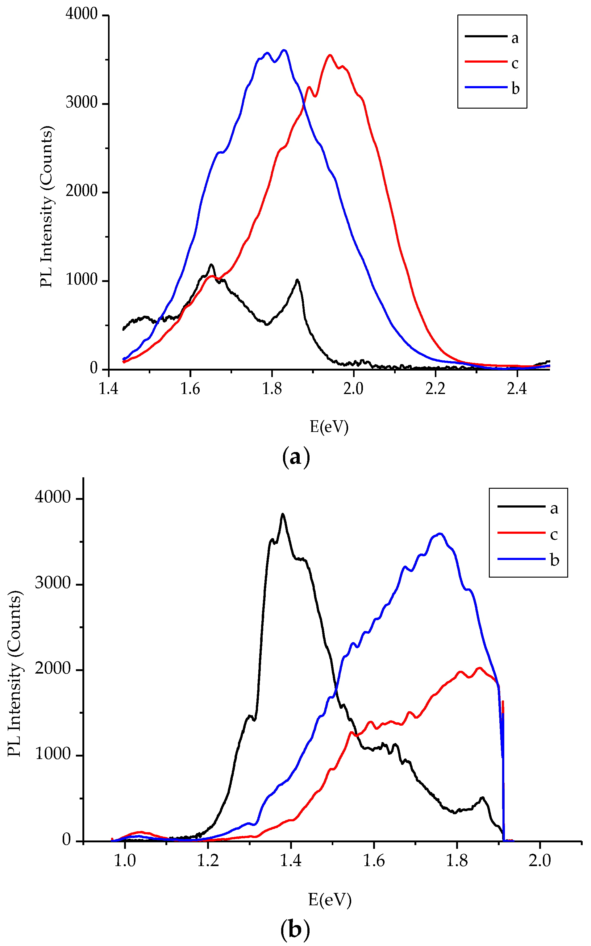
Figure 14.
The photoluminescence spectra of CdS1−yTey thin films measured at −213 °C. (a) Taken by the second grating; (b) Taken by the first grating [28].
Figure 14.
The photoluminescence spectra of CdS1−yTey thin films measured at −213 °C. (a) Taken by the second grating; (b) Taken by the first grating [28].

Figure 15.
The photoluminescence spectra of the interface of CdS/CdTe solar cells. (a) taken by the second grating; (b) taken by the first grating [43].
Figure 15.
The photoluminescence spectra of the interface of CdS/CdTe solar cells. (a) taken by the second grating; (b) taken by the first grating [43].


Table 1.
The thickness t, Te molar ratio y, and percentage ratios of indium to cadmium concentrations in the precursor solution and in the films respectively.
| t (nm) | y × 10−2 | ([In]/[Cd])% in the Solution | ([In]/[Cd])% in the Film |
|---|---|---|---|
| 500 | 0 | 1.5 | 3.31 ± 0.34 |
| 490 | 3.49 ± 1.68 | 1.5 | 2.98 ± 0.20 |
| 720 | 4.51 ± 2.45 | 1.5 | 2.81 ± 0.23 |
| 260 | 4.95 ± 3.51 | 0.01 | 3.54 ± 0.43 |
| 465 | 8.52 ± 6.41 | 1.5 | 3.84 ± 0.63 |
| 420 | 9.97 ± 9.21 | 0.01 | 2.75 ± 1.88 |
| 460 | 10.02 ± 8.27 | 0.0055 | 3.08 ± 1.24 |
| 620 | 28.45 ± 2.57 | 0.01 | 3.49 ± 0.27 |
Table 2.
The values of the wavelength at the minima from Figure 7, estimated values of the bandgap energies for different values of y, film thickness, and the estimated values of the Urbach tail width Ee.
| t (nm) | y = [Te]/([Te] + [S]) 10−2 | ([In]/[Cd])% in the Film | λmin1 (nm) (Hexagonal) | Eg1(x) (eV) (Hexagonal) | λmin2 (nm) (Cubic) | Eg2 (x) (eV) (Cubic) | Ee (eV) |
|---|---|---|---|---|---|---|---|
| 500 | 0 | 3.31 ± 0.34 | 500 | 2.480 | Not estimated | ||
| 490 | 3.49 ± 1.68 | 2.98 ± 0.20 | 502.5 | 2.468 | 1.406 | ||
| 720 | 4.51 ± 2.45 | 2.81 ± 0.23 | 490 | 2.531 | 1.002 | ||
| 260 | 4.95 ± 3.51 | 3.54 ± 0.43 | 503 | 2.465 | 0.938 | ||
| 465 | 8.52 ± 6.41 | 3.84 ± 0.63 | 507 | 2.446 | 0.929 | ||
| 420 | 9.97 ± 9.21 | 2.75 ± 1.88 | 507.5 | 2.443 | 549 | 2.259 | 1.172 |
| 460 | 10.02 ± 8.27 | 3.08 ± 1.24 | 496 | 2.500 | 535 | 2.318 | 1.502 |
| 620 | 28.45 ± 2.57 | 3.49 ± 0.27 | 490.5 | 2.528 | 532 | 2.331 | 1.747 |
| t (nm) | Composition y (10−2) | n∞ | ε∞ | λ0 (nm) | E0 (eV) | Ed (eV) | M−1 (eV)−2 | M−3 (eV)−2 |
|---|---|---|---|---|---|---|---|---|
| 500 | 0 | 1.628 | 2.649 | 591.7 | 2.096 | 3.457 | 1.649 | 0.376 |
| 490 | 3.49 ± 1.68 | 2.208 | 4.873 | 591.9 | 2.095 | 8.115 | 3.873 | 0.882 |
| 465 | 8.52 ± 6.41 | 2.177 | 4.740 | 666.3 | 1.861 | 6.960 | 3.740 | 1.080 |
| 420 | 9.97 ± 9.21 | 2.548 | 6.495 | 648.9 | 1.911 | 10.500 | 5.495 | 1.505 |
| 460 | 10.02 ± 8.27 | 4.321 | 18.671 | 667.3 | 1.858 | 32.838 | 17.671 | 5.117 |
© 2016 by the author; licensee MDPI, Basel, Switzerland. This article is an open access article distributed under the terms and conditions of the Creative Commons by Attribution (CC-BY) license (http://creativecommons.org/licenses/by/4.0/).
Share and Cite
MDPI and ACS Style
Ikhmayies, S.J. S-Rich CdS1−yTey Thin Films Produced by the Spray Pyrolysis Technique. Energies 2016, 9, 234. https://doi.org/10.3390/en9040234
AMA Style
Ikhmayies SJ. S-Rich CdS1−yTey Thin Films Produced by the Spray Pyrolysis Technique. Energies. 2016; 9(4):234. https://doi.org/10.3390/en9040234
Chicago/Turabian StyleIkhmayies, Shadia J. 2016. "S-Rich CdS1−yTey Thin Films Produced by the Spray Pyrolysis Technique" Energies 9, no. 4: 234. https://doi.org/10.3390/en9040234
Note that from the first issue of 2016, this journal uses article numbers instead of page numbers. See further details here.