
Inorganic p-Type Semiconductors: Their Applications and Progress in Dye-Sensitized Solar Cells and Perovskite Solar Cells


Abstract
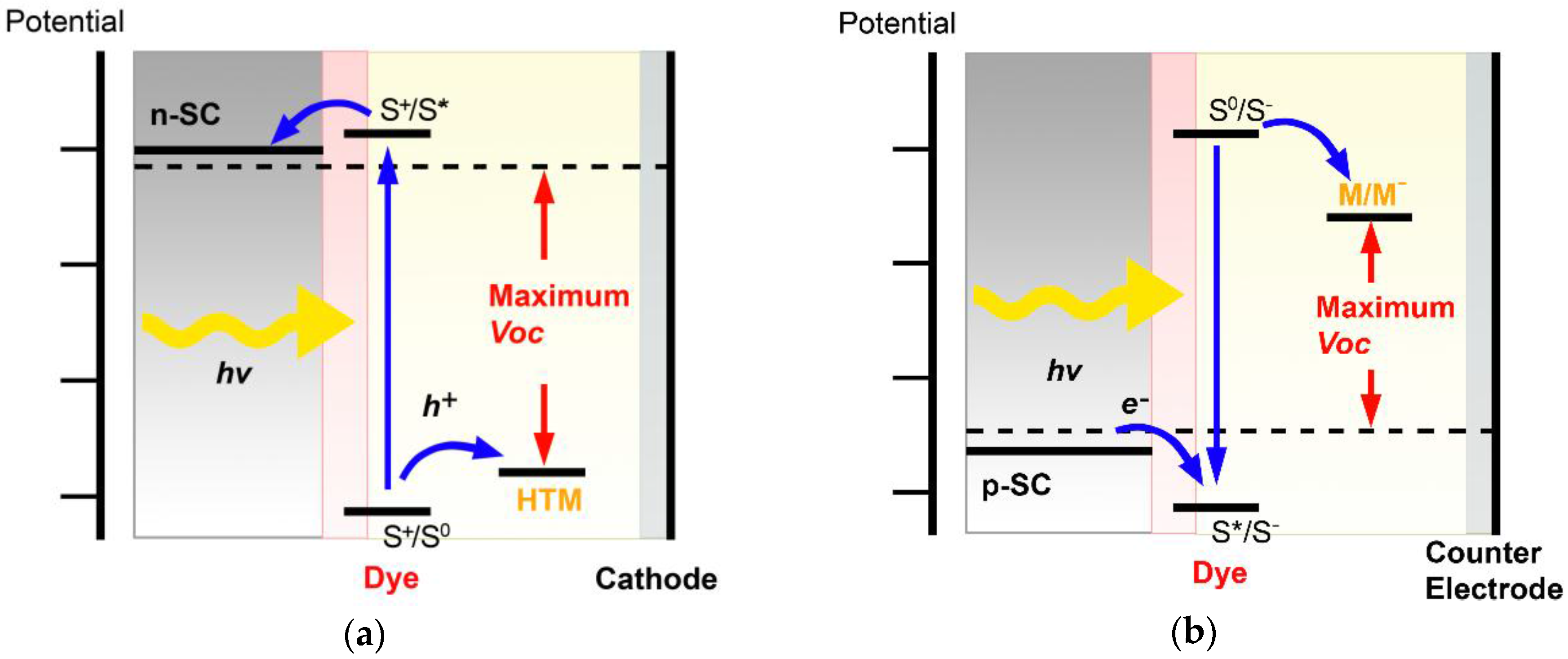
:1. Introduction
2. p-Type Hole Transport Materials for DSCs
2.1. CuSCN
2.2. CuI
2.3. CsSnI3
3. p-Type Sensitization for DSCs
3.1. NiO
3.2. Cu(I) Delafossite
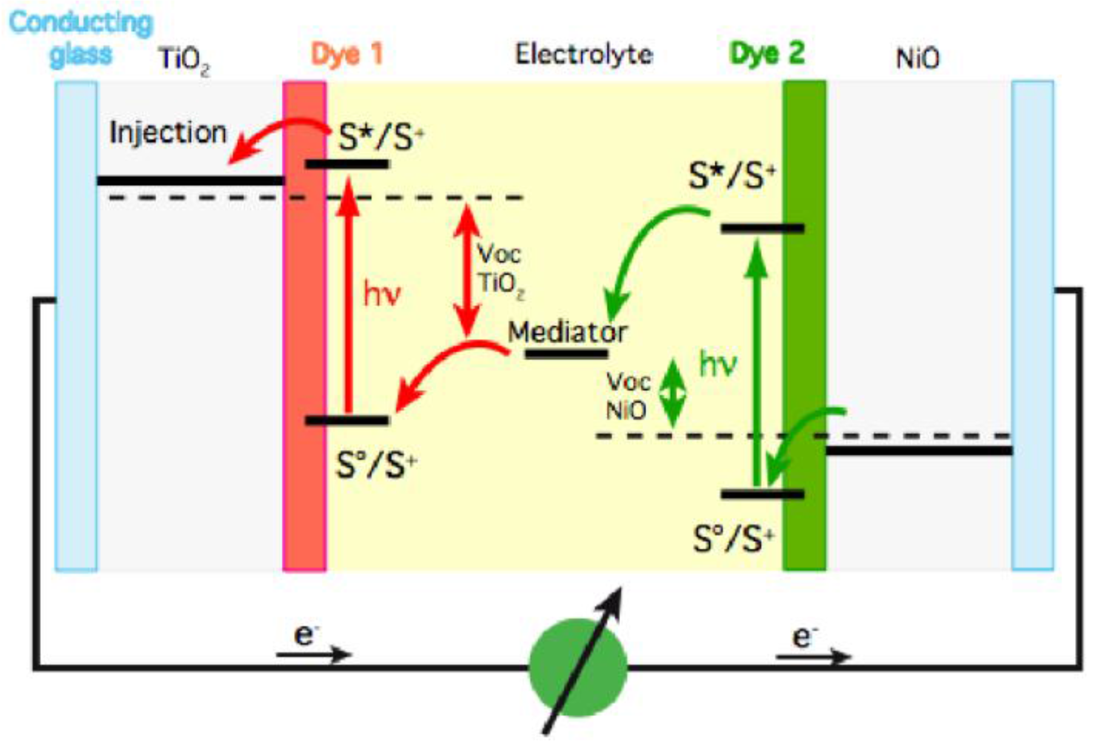
3.3. Tandems DSC
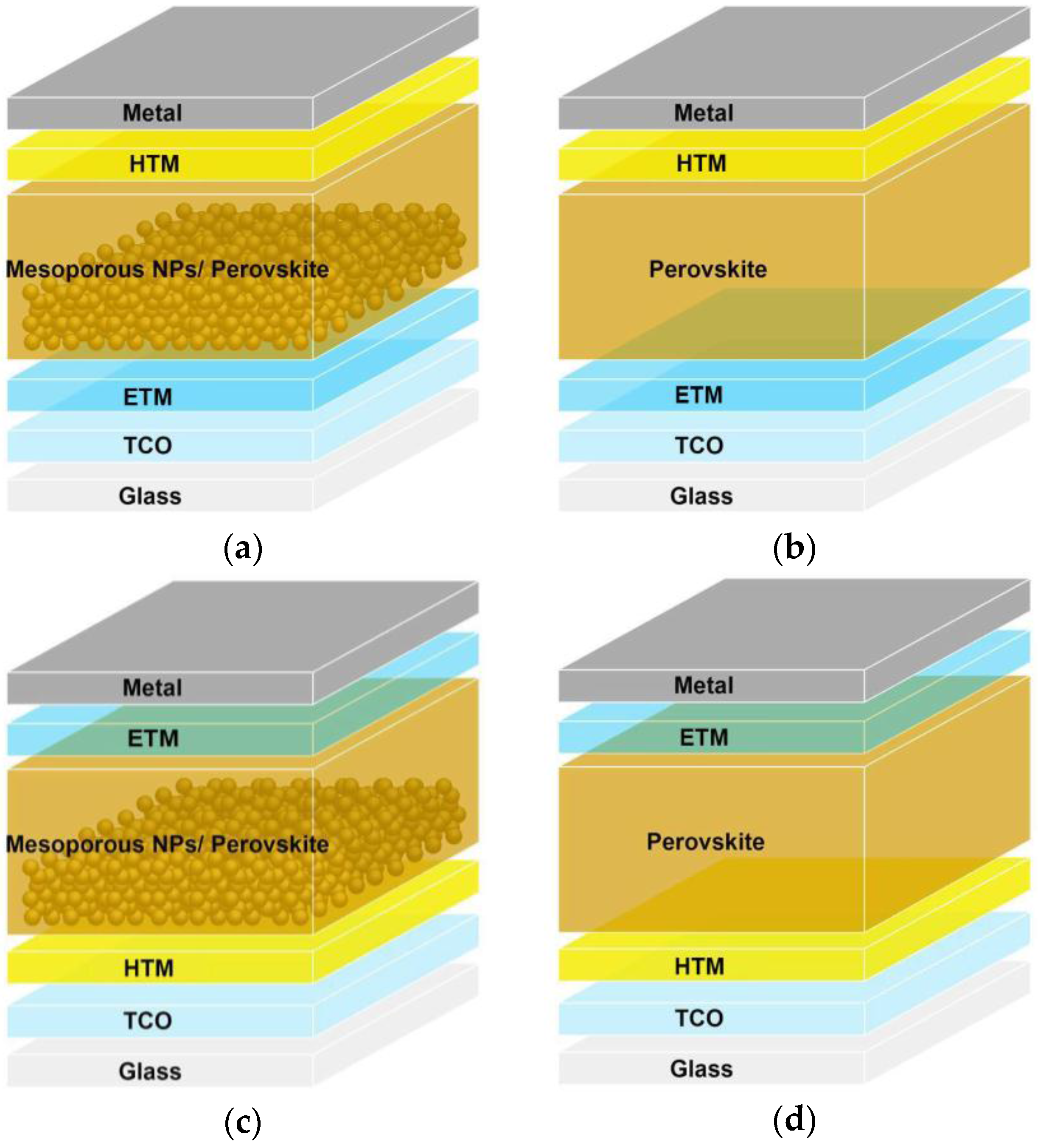
4. p-Type Inorganic Hole Transport Materials for PSCs
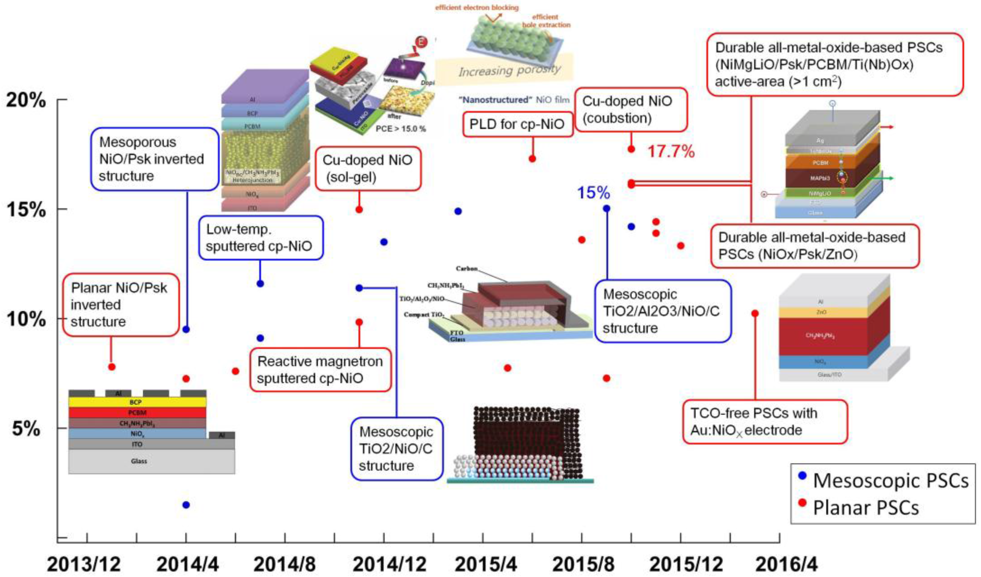
4.1. NiO
4.1.1. Mesoporous NiO-Based n-i-p PSCs
4.1.2. Planar NiO-Based n-i-p PSCs
4.1.3. Mesoporous NiO-Based p-i-n PSCs
4.1.4. Planar NiO-Based p-i-n PSCs
4.2. CuSCN
4.2.1. Meoporous CuSCN-Based n-i-p PSCs
4.2.2. Planar CuSCN-Based n-i-p PSCs
4.2.3. CuSCN-Based p-i-n PSCs
4.3. CuI
4.4. Cu2O and CuO
5. Summary
6. Future Trends
Acknowledgments
Author Contributions
Conflicts of Interest
Abbreviations
| DSC | Dye-sensitized solar cell |
| n-SC | n-Type semiconductor |
| p-SC | p-Type semiconductor |
| PSC | Organometallic lead halide perovskite solarcell |
| TCO | Transparent conductive oxide |
| D | Electron-donor |
| A | Electron-acceptor |
| π | π Conjugation |
| S | Sensitizer |
| HTM | Hole transport material |
| ETM | Electron transport material |
| SSDSC | Solid-state dye-sensitized solar cells |
| HOMO | Highest occupied molecular orbital |
| LUMO | Lowest unoccupied molecular orbital |
| IPCE | Incident photon to current conversion efficiency |
| APCE | Absorbed photon to current conversion efficiency |
| VB | Valence band |
| CB | Conduction band |
| spiro-OMeTAD | 2,2′,7,7′-Tetrakis(N,N-di-p-methoxyphenyamine)-9,9′-spirobifluorene |
| PEDOT | Poly(3,4-ethylenedioxythiophene) |
| PSS | Poly(styrene sulfonate) |
| Voc | Open circuit voltage |
| Jsc | Short circuit current density |
| FF | Fill factor |
| PCE | Power conversion efficiency (= η) |
| FTO | Fluorine-doped tin oxide |
| ITO | Indium-doped tin oxide |
| MEISCN | 1-Methyl-3-ethylimidazoliumthiocyanate |
| THT | Triethylamine hydrothiocyanate |
| LHE | Light harvesting efficiency |
| TPA | Triphenylamine |
| cp | Compact |
| mp | Mesoporous |
| dtb-bpy | di-tert-Butylbipyridine |
| P | Planar |
| Psk | Perovskite |
| BCP | Bathocuproine |
| PHJ | Planar heterojunction junction |
References
- O’Regan, B.; Grätzel, M. A low-cost, high-efficiency solar-cell based on dye-sensitized colloidal TiO2 films. Nature 1991, 353, 737–740. [Google Scholar] [CrossRef]
- Hagfeldt, A.; Grätzel, M. Light-induced redox reactions in nanocrystalline systems. Chem. Rev. 1995, 95, 49–68. [Google Scholar] [CrossRef]
- Hagfeldt, A.; Grätzel, M. Molecular photovoltaics. Acc. Chem. Res. 2000, 33, 269–277. [Google Scholar] [CrossRef] [PubMed]
- Grätzel, M. Photoelectrochemical cells. Nature 2001, 414, 338–344. [Google Scholar] [CrossRef] [PubMed]
- Goncalves, L.M.; Bermudez, V.D.; Ribeiro, H.A.; Mendes, A.M. Dye-sensitized solar cells: A safe bet for the future. Energy Environ. Sci. 2008, 1, 655–667. [Google Scholar] [CrossRef]
- Hardin, B.E.; Snaith, H.J.; McGehee, M.D. The renaissance of dye-sensitized solar cells. Nat. Photonics 2012, 6, 162–169. [Google Scholar] [CrossRef]
- Yella, A.; Lee, H.W.; Tsao, H.N.; Yi, C.Y.; Chandiran, A.K.; Nazeeruddin, M.K.; Diau, E.W.G.; Yeh, C.Y.; Zakeeruddin, S.M.; Grätzel, M. Porphyrin-sensitized solar cells with cobalt (II/III)-based redox electrolyte exceed 12 percent efficiency. Science 2011, 334, 629–634. [Google Scholar] [CrossRef] [PubMed]
- Kakiage, K.; Aoyama, Y.; Yano, T.; Otsuka, T.; Kyomen, T.; Unno, M.; Hanaya, M. An achievement of over 12 percent efficiency in an organic dye-sensitized solar cell. Chem. Commun. 2014, 50, 6379–6381. [Google Scholar] [CrossRef] [PubMed]
- Mathew, S.; Yella, A.; Gao, P.; Humphry-Baker, R.; Curchod, B.F.E.; Ashari-Astani, N.; Tavernelli, I.; Rothlisberger, U.; Nazeeruddin, M.K.; Grätzel, M. Dye-sensitized solar cells with 13% efficiency achieved through the molecular engineering of porphyrin sensitizers. Nat. Chem. 2014, 6, 242–247. [Google Scholar] [CrossRef] [PubMed]
- Ozawa, H.; Okuyama, Y.; Arakawa, H. Dependence of the efficiency improvement of black-dyebased dye-sensitized solar cells on alkyl chain length of quaternary ammonium cations in electrolyte solutions. ChemPhysChem. 2014, 15, 1201–1206. [Google Scholar] [CrossRef] [PubMed]
- Kakiage, K.; Aoyama, Y.; Yano, T.; Oya, K.; Kyomen, T.; Hanaya, M. Fabrication of a high-performance dye-sensitized solar cell with 12.8% conversion efficiency using organic silyl-anchor dyes. Chem. Commun. 2015, 51, 6315–6317. [Google Scholar] [CrossRef] [PubMed]
- Poplavskyy, D.; Nelson, J. Nondispersive hole transport in amorphous films of methoxy-spirofluorene-arylamine organic compound. J. Appl. Phys. 2003, 93, 341–346. [Google Scholar] [CrossRef]
- Bach, U.; Lupo, D.; Comte, P.; Moser, J.E.; Weissortel, F.; Salbeck, J.; Spreitzer, H.; Grätzel, M. Solid-state dye-sensitized mesoporous TiO2 solar cells with high photon-to-electron conversion efficiencies. Nature 1998, 395, 583–585. [Google Scholar]
- Kruger, J.; Plass, R.; Cevey, L.; Piccirelli, M.; Grätzel, M.; Bach, U. High efficiency solid-state photovoltaic device due to inhibition of interface charge recombination. Appl. Phys. Lett. 2001, 79, 2085–2087. [Google Scholar] [CrossRef]
- Schmidt-Mende, L.; Bach, U.; Humphry-Baker, R.; Horiuchi, T.; Miura, H.; Ito, S.; Uchida, S.; Gratzel, M. Organic dye for highly efficient solid-state dye-sensitized solar cells. Adv. Mater. 2005, 17, 813–815. [Google Scholar] [CrossRef]
- Snaith, H.J.; Moule, A.J.; Klein, C.; Meerholz, K.; Friend, R.H.; Grätzel, M. Efficiency enhancements in solid-state hybrid solar cells via reduced charge recombination and increased light capture. Nano Lett. 2007, 7, 3372–3376. [Google Scholar] [CrossRef] [PubMed]
- Karthikeyan, C.S.; Wietasch, H.; Thelakkat, M. Highly efficient solid-state dye-sensitized TiO2 solar cells using donor-antenna dyes capable of multistep charge-transfer cascades. Adv. Mater. 2007, 19, 1091–1095. [Google Scholar] [CrossRef]
- Cai, N.; Moon, S.J.; Cevey-Ha, L.; Moehl, T.; Humphry-Baker, R.; Wang, P.; Zakeeruddin, S.M.; Grätzel, M. An organic D-pi-A dye for record efficiency solid-state sensitized heterojunction solar cells. Nano Lett. 2011, 11, 1452–1456. [Google Scholar] [CrossRef] [PubMed]
- Burschka, J.; Dualeh, A.; Kessler, F.; Baranoff, E.; Cevey-Ha, N.L.; Yi, C.Y.; Nazeeruddin, M.K.; Grätzel, M. Tris(2-(1H-pyrazol-1-yl)pyridine)cobalt(III) as p-type dopant for organic semiconductors and its application in highly efficient solid-state dye-sensitized solar cells. J. Am. Chem. Soc. 2011, 133, 18042–18045. [Google Scholar] [CrossRef] [PubMed]
- Tan, M.X.; Laibinis, P.E.; Nguyen, S.T.; Kesselman, J.M.; Stanton, C.E.; Lewis, N.S. Principles and applications of semiconductor photoelectrochemistry. Prog. Inorg. Chem. 1994, 41, 21–144. [Google Scholar]
- Hagfeldt, A.; Boschloo, G.; Sun, L.C.; Kloo, L.; Pettersson, H. Dye-sensitized solar cells. Chem. Rev. 2010, 110, 6595–6663. [Google Scholar] [CrossRef] [PubMed]
- Patzke, G.R.; Zhou, Y.; Kontic, R.; Conrad, F. Oxide nanomaterials: Synthetic developments, mechanistic studies, and technological innovations. Angew. Chem. Int. Ed. 2011, 50, 826–859. [Google Scholar] [CrossRef] [PubMed]
- Loh, L.; Dunn, S. Recent progress in ZnO-based nanostructured ceramics in solar cell applications. J. Nanosci. Nanotechnol. 2012, 12, 8215–8230. [Google Scholar] [CrossRef] [PubMed]
- Wali, Q.; Fakharuddin, A.; Jose, R. Tin oxide as a photoanode for dye-sensitised solar cells: Current progress and future challenges. J. Power Sources 2015, 293, 1039–1052. [Google Scholar] [CrossRef]
- Gibson, E.A.; Smeigh, A.L.; Le Pleux, L.; Fortage, J.; Boschloo, G.; Blart, E.; Pellegrin, Y.; Odobel, F.; Hagfeldt, A.; Hammarstrom, L. A p-type NiO-based dye-sensitized solar cell with an open-circuit voltage of 0.35 V. Angew. Chem. Int. Ed. 2009, 48, 4402–4405. [Google Scholar] [CrossRef] [PubMed]
- Odobel, F.; Le Pleux, L.; Pellegrin, Y.; Blart, E. New photovoltaic devices based on the sensitization of p-type semiconductors: Challenges and opportunities. Acc. Chem. Res. 2010, 43, 1063–1071. [Google Scholar] [CrossRef] [PubMed]
- Nattestad, A.; Mozer, A.J.; Fischer, M.K.R.; Cheng, Y.B.; Mishra, A.; Bauerle, P.; Bach, U. Highly efficient photocathodes for dye-sensitized tandem solar cells. Nat. Mater. 2010, 9, 31–35. [Google Scholar] [CrossRef] [PubMed]
- Yang, W.S.; Noh, J.H.; Jeon, N.J.; Kim, Y.C.; Ryu, S.; Seo, J.; Seok, S.I. High-performance photovoltaic perovskite layers fabricated through intramolecular exchange. Science 2015, 348, 1234–1237. [Google Scholar] [CrossRef] [PubMed]
- Kim, H.-S.; Lee, C.-R.; Im, J.-H.; Lee, K.-B.; Moehl, T.; Marchioro, A.; Moon, S.-J.; Humphry-Baker, R.; Yum, J.-H.; Moser, J.E.; et al. Lead iodide perovskite sensitized all-solid-state submicron thin film mesoscopic solar cell with efficiency exceeding 9%. Sci. Rep. 2012, 2. [Google Scholar] [CrossRef] [PubMed]
- Yu, Z.; Sun, L. Recent progress on hole-transporting materials for emerging organometal halide perovskite solar cells. Adv. Energy Mater. 2015, 5. [Google Scholar] [CrossRef]
- Salim, T.; Sun, S.; Abe, Y.; Krishna, A.; Grimsdale, A.C.; Lam, Y.M. Perovskite-based solar cells: Impact of morphology and device architecture on device performance. J. Mater. Chem. A 2015, 3, 8943–8969. [Google Scholar] [CrossRef]
- Heo, J.H.; Han, H.J.; Kim, D.; Ahn, T.K.; Im, S.H. Hysteresis-less inverted CH3NH3PbI3 planar perovskite hybrid solar cells with 18.1% power conversion efficiency. Energy Environ. Sci. 2015, 8, 1602–1608. [Google Scholar] [CrossRef]
- You, J.; Meng, L.; Song, T.-B.; Guo, T.-F.; Yang, Y.; Chang, W.-H.; Hong, Z.; Chen, H.; Zhou, H.; Chen, Q.; et al. Improved air stability of perovskite solar cells via solution-processed metal oxide transport layers. Nat. Nanotechnol. 2016, 11, 75–81. [Google Scholar] [CrossRef] [PubMed]
- Chen, W.; Wu, Y.; Yue, Y.; Liu, J.; Zhang, W.; Yang, X.; Chen, H.; Bi, E.; Ashraful, I.; Grätzel, M.; et al. Efficient and stable large-area perovskite solar cells with inorganic charge extraction layers. Science 2015, 350, 944–948. [Google Scholar] [CrossRef] [PubMed]
- Trifiletti, V.; Roiati, V.; Colella, S.; Giannuzzi, R.; De Marco, L.; Rizzo, A.; Manca, M.; Listorti, A.; Gigli, G. NiO/MAPbI3−xClx/PCBM: A model case for an improved understanding of inverted mesoscopic solar cells. ACS Appl. Mater. Interfaces 2015, 7, 4283–4289. [Google Scholar] [CrossRef] [PubMed]
- Nejand, B.A.; Ahmadi, V.; Shahverdi, H.R. New physical deposition approach for low cost inorganic hole transport layer in normal architecture of durable perovskite solar cells. ACS Appl. Mater. Interfaces 2015, 7, 21807–21818. [Google Scholar] [CrossRef] [PubMed]
- Li, D.M.; Qin, D.; Deng, M.H.; Luo, Y.H.; Meng, Q.B. Optimization the solid-state electrolytes for dye-sensitized solar cells. Energy Environ. Sci. 2009, 2, 283–291. [Google Scholar] [CrossRef]
- Schmidt-Mende, L.; Gratzel, M. TiO2 pore-filling and its effect on the efficiency of solid-state dye-sensitized solar cells. Thin Solid Films 2006, 500, 296–301. [Google Scholar] [CrossRef]
- Snaith, H.J.; Schmidt-Mende, L. Advances in liquid-electrolyte and solid-state dye-sensitized solar cells. Adv. Mater. 2007, 19, 3187–3200. [Google Scholar] [CrossRef]
- Ding, I.K.; Tetreault, N.; Brillet, J.; Hardin, B.E.; Smith, E.H.; Rosenthal, S.J.; Sauvage, F.; Gratzel, M.; McGehee, M.D. Pore-filling of spiro-ometad in solid-state dye sensitized solar cells: Quantification, mechanism, and consequences for device performance. Adv. Funct. Mater. 2009, 19, 2431–2436. [Google Scholar] [CrossRef]
- Wu, J.H.; Lan, Z.; Lin, J.M.; Huang, M.L.; Huang, Y.F.; Fan, L.Q.; Luo, G.G. Electrolytes in dye-sensitized solar cells. Chem. Rev. 2015, 115, 2136–2173. [Google Scholar] [CrossRef] [PubMed]
- Smith, D.L.; Saunders, V.I. The structure and polytypism of the beta-modification of copper(I) thiocyanate. Acta. Crystallogr. B 1981, 37, 1807–1812. [Google Scholar] [CrossRef]
- Hehl, R.; Thiele, G. Synthesis and crystal structure of Me3NHCu2(SCN)3, Me2C = NMe2Cu2(SCN)3, and Me2C = NMe2Ag2(SCN)3. Three-dimensional networks of thiocyanatometallates(I). Z. Anorg. Allg. Chem. 2000, 626, 2167–2172. [Google Scholar] [CrossRef]
- Nilushi, W.; Thomas, D.A. Copper(I) thiocyanate (CuSCN) as a hole-transport material for large-area opto/electronics. Semicond. Sci. Technol. 2015, 30, 104002. [Google Scholar] [CrossRef]
- O’Regan, B.; Schwartz, D.T. Efficient dye-sensitized charge separation in a wide-band-gap p-n heterojunction. J. Appl. Phys. 1996, 80, 4749–4754. [Google Scholar] [CrossRef]
- Kumara, G.R.R.A.; Konno, A.; Senadeera, G.K.R.; Jayaweera, P.V.V.; De Silva, D.B.R.A.; Tennakone, K. Dye-sensitized solar cell with the hole collector p-CuSCN deposited from a solution in n-propyl sulphide. Sol. Energy Mater. Sol. Cells 2001, 69, 195–199. [Google Scholar] [CrossRef]
- O’regan, B.; Lenzmann, F.; Muis, R.; Wienke, J. A solid-state dye-sensitized solar cell fabricated with pressure-treated P25-TiO2 and CuSCN: Analysis of pore filling and iv characteristics. Chem. Mater. 2002, 14, 5023–5029. [Google Scholar] [CrossRef]
- O’Regan, B.C.; Lenzmann, F. Charge transport and recombination in a nanoscale interpenetrating network of n-type and p-type semiconductors: Transient photocurrent and photovoltage studies of TiO2/dye/CuSCN photovoltaic cells. J. Phys. Chem. B 2004, 108, 4342–4350. [Google Scholar] [CrossRef]
- O’Regan, B.C.; Scully, S.; Mayer, A.C.; Palomares, E.; Durrant, J. The effect of Al2O3 barrier layers in TiO2/dye/CuSCN photovoltaic cells explored by recombination and dos characterization using transient photovoltage measurements. J. Phys. Chem. B 2005, 109, 4616–4623. [Google Scholar] [CrossRef] [PubMed]
- Ranasinghe, C.S.K.; Jayaweera, E.N.; Kumara, G.R.A.; Rajapakse, R.M.G.; Onwona-Agyeman, B.; Perera, A.G.U.; Tennakone, K. Tin oxide based dye-sensitized solid-state solar cells: Surface passivation for suppression of recombination. Mater. Sci. Semicon. Proc. 2015, 40, 890–895. [Google Scholar] [CrossRef]
- Perera, V.P.S.; Senevirathna, M.K.I.; Pitigala, P.K.D.D.P.; Tennakone, K. Doping cuscn films for enhancement of conductivity: Application in dye-sensitized solid-state solar cells. Sol. Energy Mater. Sol. Cells 2005, 86, 443–450. [Google Scholar] [CrossRef]
- Premalal, E.V.A.; Kumara, G.R.R.A.; Rajapakse, R.M.G.; Shimomura, M.; Murakami, K.; Konno, A. Tuning chemistry of CuSCN to enhance the performance of TiO2/N719/CuSCN all-solid-state dye-sensitized solar cell. Chem. Commun. 2010, 46, 3360–3362. [Google Scholar] [CrossRef] [PubMed]
- Premalal, E.V.A.; Dematage, N.; Kumara, G.R.R.A.; Rajapakse, R.M.G.; Shimomura, M.; Murakami, K.; Konno, A. Preparation of structurally modified, conductivity enhanced-p-CuSCN and its application in dye-sensitized solid-state solar cells. J. Power Sources 2012, 203, 288–296. [Google Scholar] [CrossRef]
- Tennakone, K.; Kumara, G.R.R.A.; Kumarasinghe, A.R.; Wijayantha, K.G.U.; Sirimanne, P.M. A dye-sensitized nano-porous solid-state photovoltaic cell. Semicond. Sci. Technol. 1995, 10, 1689–1693. [Google Scholar] [CrossRef]
- Tennakone, K.; Kumara, G.R.R.A.; Kottegoda, I.R.M.; Wijayantha, K.G.U.; Perera, V.P.S. A solid-state photovoltaic cell sensitized with a ruthenium bipyridyl complex. J. Phys. D Appl. Phys. 1998, 31, 1492–1496. [Google Scholar] [CrossRef]
- Kumara, G.R.A.; Konno, A.; Shiratsuchi, K.; Tsukahara, J.; Tennakone, K. Dye-sensitized solid-state solar cells: Use of crystal growth inhibitors for deposition of the hole collector. Chem. Mater. 2002, 14, 954–955. [Google Scholar] [CrossRef]
- Meng, Q.B.; Takahashi, K.; Zhang, X.T.; Sutanto, I.; Rao, T.N.; Sato, O.; Fujishima, A.; Watanabe, H.; Nakamori, T.; Uragami, M. Fabrication of an efficient solid-state dye-sensitized solar cell. Langmuir 2003, 19, 3572–3574. [Google Scholar] [CrossRef]
- Kumara, G.R.A.; Kaneko, S.; Okuya, M.; Tennakone, K. Fabrication of dye-sensitized solar cells using triethylamine hydrothiocyanate as a CuI crystal growth inhibitor. Langmuir 2002, 18, 10493–10495. [Google Scholar] [CrossRef]
- Taguchi, T.; Zhang, X.T.; Sutanto, I.; Tokuhiro, K.; Rao, T.N.; Watanabe, H.; Nakamori, T.; Uragami, M.; Fujishima, A. Improving the performance of solid-state dye-sensitized solar cell using mgo-coated TiO2 nanoporous film. Chem. Commun. 2003, 9, 2480–2481. [Google Scholar] [CrossRef]
- Kumara, G.R.A.; Okuya, M.; Murakami, K.; Kaneko, S.; Jayaweera, V.V.; Tennakone, K. Dye-sensitized solid-state solar cells made from magnesiumoxide-coated nanocrystalline titanium dioxide films: Enhancement of the efficiency. J. Photochem. Photobiol. A 2004, 164, 183–185. [Google Scholar] [CrossRef]
- Mahrov, B.; Boschloo, G.; Hagfeldt, A.; Siegbahn, H.; Rensmo, H. Photoelectron spectroscopy studies of Ru(dcbpyH2)2(NCS)2/CuI and Ru(dcbpyH2)2(NCS)2/CuSCN interfaces for solar cell applications. J. Phys. Chem. B 2004, 108, 11604–11610. [Google Scholar] [CrossRef]
- Sakamoto, H.; Igarashi, S.; Niume, K.; Nagai, M. Highly efficient all solid state dye-sensitized solar cells by the specific interaction of CuI with NCS groups. Org. Electron. 2011, 12, 1247–1252. [Google Scholar] [CrossRef]
- Sakamoto, H.; Igarashi, S.; Niume, K.; Nagai, M. All solid state dye-sensitized solar cells by the specific interaction of CuI with NCS groups for practical use. J. Ceram. Soc. Jpn. 2012, 120, 304–306. [Google Scholar] [CrossRef]
- Sakamoto, H.; Igarashi, S.; Uchida, M.; Niume, K.; Nagai, M. Highly efficient all solid state dye-sensitized solar cells by the specific interaction of CuI with NCS groups II. Enhancement of the photovoltaic characteristics. Org. Electron. 2012, 13, 514–518. [Google Scholar] [CrossRef]
- Chung, I.; Lee, B.; He, J.Q.; Chang, R.P.H.; Kanatzidis, M.G. All-solid-state dye-sensitized solar cells with high efficiency. Nature 2012, 485, 486–489. [Google Scholar] [CrossRef] [PubMed]
- Chung, I.; Song, J.H.; Im, J.; Androulakis, J.; Malliakas, C.D.; Li, H.; Freeman, A.J.; Kenney, J.T.; Kanatzidis, M.G. CsSnI3: Semiconductor or metal? High electrical conductivity and strong near-infrared photoluminescence from a single material. High hole mobility and phase-transitions. J. Am. Chem. Soc. 2012, 134, 8579–8587. [Google Scholar] [CrossRef] [PubMed]
- Lee, B.; Stoumpos, C.C.; Zhou, N.J.; Hao, F.; Malliakas, C.; Yeh, C.Y.; Marks, T.J.; Kanatzidis, M.G.; Chang, R.P.H. Air-stable molecular semiconducting lodosalts for solar cell applications: Cs2Snl6as a hole conductor. J. Am. Chem. Soc. 2014, 136, 15379–15385. [Google Scholar] [CrossRef] [PubMed]
- He, J.J.; Lindström, H.; Hagfeldt, A.; Lindquist, S.E. Dye-sensitized nanostructured p-type nickel oxide film as a photocathode for a solar cell. J. Phys. Chem. B 1999, 103, 8940–8943. [Google Scholar] [CrossRef]
- Mori, S.; Fukuda, S.; Sumikura, S.; Takeda, Y.; Tamaki, Y.; Suzuki, E.; Abe, T. Charge-transfer processes in dye-sensitized NiO solar cells. J. Phys. Chem. C 2008, 112, 16134–16139. [Google Scholar] [CrossRef]
- Li, L.; Gibson, E.A.; Qin, P.; Boschloo, G.; Gorlov, M.; Hagfeldt, A.; Sun, L.C. Double-layered NiO photocathodes for p-type DSSCs with record IPCE. Adv. Mater. 2010, 22, 1759–1762. [Google Scholar] [CrossRef] [PubMed]
- Qin, P.; Zhu, H.J.; Edvinsson, T.; Boschloo, G.; Hagfeldt, A.; Sun, L.C. Design of an organic chromophore for p-type dye-sensitized solar cells. J. Am. Chem. Soc. 2008, 130, 8570–8571. [Google Scholar] [CrossRef] [PubMed]
- Sumikura, S.; Mori, S.; Shimizu, S.; Usami, H.; Suzuki, E. Syntheses of NiO nanoporous films using nonionic triblock co-polymer templates and their application to photo-cathodes of p-type dye-sensitized solar cells. J. Photochem. Photobiol. A 2008, 199, 1–7. [Google Scholar] [CrossRef]
- Awais, M.; Rahman, M.; MacElroy, J.M.D.; Dini, D.; Vos, J.G.; Dowling, D.P. Application of a novel microwave plasma treatment for the sintering of nickel oxide coatings for use in dye-sensitized solar cells. Surf. Coat. Technol. 2011, 205, S245–S249. [Google Scholar] [CrossRef]
- Powar, S.; Wu, Q.; Weidelener, M.; Nattestad, A.; Hu, Z.; Mishra, A.; Bauerle, P.; Spiccia, L.; Cheng, Y.B.; Bach, U. Improved photocurrents for p-type dye-sensitized solar cells using nano-structured nickel(II) oxide microballs. Energy Environ. Sci. 2012, 5, 8896–8900. [Google Scholar] [CrossRef]
- Zhang, X.L.; Zhang, Z.P.; Huang, F.Z.; Bauerle, P.; Bach, U.; Cheng, Y.B. Charge transport in photocathodes based on the sensitization of NiO nanorods. J. Mater. Chem. 2012, 22, 7005–7009. [Google Scholar] [CrossRef]
- Gibson, E.A.; Awais, M.; Dini, D.; Dowling, D.P.; Pryce, M.T.; Vos, J.G.; Boschloo, G.; Hagfeldt, A. Dye sensitised solar cells with nickel oxide photocathodes prepared via scalable microwave sintering. Phys. Chem. Chem. Phys. 2013, 15, 2411–2420. [Google Scholar] [CrossRef] [PubMed]
- Wood, C.J.; Summers, G.H.; Clark, C.A.; Kaeffer, N.; Braeutigam, M.; Carbone, L.R.; D'Amario, L.; Fan, K.; Farré, Y.; Narbey, S.; et al. A comprehensive comparison of dye-sensitized nio photocathodes for solar energy conversion. Phys. Chem. Chem. Phys. 2016, 18, 10727–10738. [Google Scholar] [CrossRef] [PubMed] [Green Version]
- Law, M.; Greene, L.E.; Johnson, J.C.; Saykally, R.; Yang, P.D. Nanowire dye-sensitized solar cells. Nat. Mater. 2005, 4, 455–459. [Google Scholar] [CrossRef] [PubMed]
- Zhang, L.; Boschloo, G.; Hammarstrom, L.; Tian, H. Solid state p-type dye-sensitized solar cells: Concept, experiment and mechanism. Phys. Chem. Chem. Phys. 2016, 18, 5080–5085. [Google Scholar] [CrossRef] [PubMed]
- Fernando, C.A.N.; Kitagawa, A.; Suzuki, M.; Takahashi, K.; Komura, T. Photoelectrochemical properties of rhodamine-C18 sensitized p-CuSCN photoelectrochemical cell (PEC). Sol. Energy Mater. Sol. Cells 1994, 33, 301–315. [Google Scholar] [CrossRef]
- Oregan, B.; Schwartz, D.T. Efficient photo-hole injection from adsorbed cyanine dyes into electrodeposited copper(I) thiocyanate thin-films. Chem. Mater. 1995, 7, 1349–1354. [Google Scholar] [CrossRef]
- Sumikura, S.; Mori, S.; Shimizu, S.; Usami, H.; Suzuki, E. Photoelectrochemical characteristics of cells with dyed and undyed nanoporous p-type semiconductor cuo electrodes. J. Photochem. Photobiol. A 2008, 194, 143–147. [Google Scholar] [CrossRef]
- Chitambar, M.; Wang, Z.J.; Liu, Y.M.; Rockett, A.; Maldonado, S. Dye-sensitized photocathodes: Efficient light-stimulated hole injection into p-gap under depletion conditions. J. Am. Chem. Soc. 2012, 134, 10670–10681. [Google Scholar] [CrossRef] [PubMed]
- Kawazoe, H.; Yasukawa, M.; Hyodo, H.; Kurita, M.; Yanagi, H.; Hosono, H. P-type electrical conduction in transparent thin films of CuAlO2. Nature 1997, 389, 939–942. [Google Scholar] [CrossRef]
- Benko, F.A.; Koffyberg, F.P. The optical interband-transitions of the semiconductor CuGaO2. Phys. Status Solidi A 1986, 94, 231–234. [Google Scholar] [CrossRef]
- Yu, M.Z.; Draskovic, T.I.; Wu, Y.Y. Cu(I)-based delafossite compounds as photocathodes in p-type dye-sensitized solar cells. Phys. Chem. Chem. Phys. 2014, 16, 5026–5033. [Google Scholar] [CrossRef] [PubMed]
- Nattestad, A.; Zhang, X.L.; Bach, U.; Cheng, Y.B. Dye-sensitized CuAlO2 photocathodes for tandem solar cell applications. J. Photonics Energy 2011, 1. [Google Scholar] [CrossRef]
- Renaud, A.; Chavillon, B.; Le Pleux, L.; Pellegrin, Y.; Blart, E.; Boujtita, M.; Pauporte, T.; Cario, L.; Jobic, S.; Odobel, F. CuGaO2: A promising alternative for NiO in p-type dye solar cells. J. Mater. Chem. 2012, 22, 14353–14356. [Google Scholar] [CrossRef]
- Ahmed, J.; Blakely, C.K.; Prakash, J.; Bruno, S.R.; Yu, M.Z.; Wu, Y.Y.; Poltavets, V.V. Scalable synthesis of delafossite CuAlO2 nanoparticles for p-type dye-sensitized solar cells applications. J. Alloy. Compd. 2014, 591, 275–279. [Google Scholar] [CrossRef]
- Xu, Z.; Xiong, D.H.; Wang, H.; Zhang, W.J.; Zeng, X.W.; Ming, L.Q.; Chen, W.; Xu, X.B.; Cui, J.; Wang, M.K.; et al. Remarkable photocurrent of p-type dye-sensitized solar cell achieved by size controlled CuGaO2 nanoplates. J. Mater. Chem. A 2014, 2, 2968–2976. [Google Scholar] [CrossRef]
- Xu, X.B.; Zhang, B.Y.; Cui, J.; Xiong, D.H.; Shen, Y.; Chen, W.; Sun, L.C.; Cheng, Y.B.; Wang, M.K. Efficient p-type dye-sensitized solar cells based on disulfide/thiolate electrolytes. Nanoscale 2013, 5, 7963–7969. [Google Scholar] [CrossRef] [PubMed]
- Ursu, D.; Vaszilcsin, N.; Banica, R.; Miclau, M. Effect of Al doping on performance of CuGaO2 p-type dye-sensitized solar cells. J. Mater. Eng. Perform. 2016, 25, 59–63. [Google Scholar] [CrossRef]
- Ursu, D.; Miclau, M.; Banica, R.; Vaszilcsin, N. Impact of Fe doping on performances of CuGaO2 p-type dye-sensitized solar cells. Mater. Lett. 2015, 143, 91–93. [Google Scholar] [CrossRef]
- Xiong, D.H.; Zhang, W.J.; Zeng, X.W.; Xu, Z.; Chen, W.; Cui, J.; Wang, M.K.; Sun, L.C.; Cheng, Y.B. Enhanced performance of p-type dye-sensitized solar cells based on ultrasmall Mg-doped CuCrO2 nanocrystals. ChemSusChem. 2013, 6, 1432–1437. [Google Scholar] [CrossRef] [PubMed]
- Renaud, A.; Cario, L.; Deniard, P.; Gautron, E.; Rocquefelte, X.; Pellegrin, Y.; Blart, E.; Odobel, F.; Jobic, S. Impact of Mg doping on performances of CuGaO2 based p-type dye-sensitized solar cells. J. Phys. Chem. C 2014, 118, 54–59. [Google Scholar] [CrossRef]
- Xiong, D.H.; Zhang, Q.Q.; Verma, S.K.; Li, H.; Chen, W.; Zhao, X.J. Use of delafossite oxides CuCr1−xGaxO2 nanocrystals in p-type dye-sensitized solar cell. J. Alloy. Compd. 2016, 662, 374–380. [Google Scholar] [CrossRef]
- Yum, J.-H.; Baranoff, E.; Wenger, S.; Nazeeruddin, M.K.; Grätzel, M. Panchromatic engineering for dye-sensitized solar cells. Energy Environ. Sci. 2010, 4, 842–857. [Google Scholar] [CrossRef]
- He, J.; Lindström, H.; Hagfeldt, A.; Lindquist, S.-E. Dye-sensitized nanostructured tandem cell-first demonstrated cell with a dye-sensitized photocathode. Sol. Energy Mater. Sol. Cells 2000, 62, 265–273. [Google Scholar] [CrossRef]
- Nakasa, A.; Suzuki, E.; Usami, H.; Fujimatsu, H. Synthesis of porous nickel oxide nanofiber. Chem. Lett. 2005, 34, 428–429. [Google Scholar] [CrossRef]
- Docampo, P.; Ball, J.M.; Darwich, M.; Eperon, G.E.; Snaith, H.J. Efficient organometal trihalide perovskite planar-heterojunction solar cells on flexible polymer substrates. Nat. Commun. 2013, 4. [Google Scholar] [CrossRef] [PubMed]
- Burschka, J.; Pellet, N.; Moon, S.-J.; Humphry-Baker, R.; Gao, P.; Nazeeruddin, M.K.; Grätzel, M. Sequential deposition as a route to high-performance perovskite-sensitized solar cells. Nature 2013, 499, 316–319. [Google Scholar] [CrossRef] [PubMed]
- Liu, Z.; Zhang, M.; Xu, X.; Bu, L.; Zhang, W.; Li, W.; Zhao, Z.; Wang, M.; Cheng, Y.-B.; He, H. P-type mesoscopic NiO as an active interfacial layer for carbon counter electrode based perovskite solar cells. Dalton Trans. 2015, 44, 3967–3973. [Google Scholar] [CrossRef] [PubMed]
- Liu, Z.; Zhang, M.; Xu, X.; Cai, F.; Yuan, H.; Bu, L.; Li, W.; Zhu, A.; Zhao, Z.; Wang, M.; et al. NiO nanosheets as efficient top hole transporters for carbon counter electrode based perovskite solar cells. J. Mater. Chem. 2015, 3, 24121–24127. [Google Scholar] [CrossRef]
- Xu, X.; Liu, Z.; Zuo, Z.; Zhang, M.; Zhao, Z.; Shen, Y.; Zhou, H.; Chen, Q.; Yang, Y.; Wang, M. Hole selective NiO contact for efficient perovskite solar cells with carbon electrode. Nano Lett. 2015, 15, 2402–2408. [Google Scholar] [CrossRef] [PubMed]
- Cao, K.; Zuo, Z.; Cui, J.; Shen, Y.; Moehl, T.; Zakeeruddin, S.M.; Grätzel, M.; Wang, M. Efficient screen printed perovskite solar cells based on mesoscopic TiO2/Al2O3/NiO/carbon architecture. Nano Energy 2015, 17, 171–179. [Google Scholar] [CrossRef]
- Tian, H.; Xu, B.; Chen, H.; Johansson, E.M.J.; Boschloo, G. Solid-state perovskite-sensitized p-type mesoporous nickel oxide solar cells. ChemSusChem. 2014, 7, 2150–2153. [Google Scholar] [CrossRef] [PubMed]
- Wang, K.-C.; Jeng, J.-Y.; Shen, P.-S.; Chang, Y.-C.; Diau, E.W.-G.; Tsai, C.-H.; Chao, T.-Y.; Hsu, H.-C.; Lin, P.-Y.; Chen, P.; et al. p-Type mesoscopic nickel oxide/organometallic perovskite heterojunction solar cells. Sci. Rep. 2014, 4. [Google Scholar] [CrossRef] [PubMed]
- Jeng, J.-Y.; Chen, K.-C.; Chiang, T.-Y.; Lin, P.-Y.; Tsai, T.-D.; Chang, Y.-C.; Guo, T.-F.; Chen, P.; Wen, T.-C.; Hsu, Y.-J. Nickel oxide electrode interlayer in CH3NH3PbI3 perovskite/pcbm planar-heterojunction hybrid solar cells. Adv. Mater. 2014, 26, 4107–4113. [Google Scholar] [CrossRef] [PubMed]
- Zhu, Z.; Bai, Y.; Zhang, T.; Liu, Z.; Long, X.; Wei, Z.; Wang, Z.; Zhang, L.; Wang, J.; Yan, F.; et al. High-performance hole-extraction layer of sol-gel-processed NiO nanocrystals for inverted planar perovskite solar cells. Angew. Chem. Int. Ed. 2014, 53, 12571–12575. [Google Scholar]
- Wang, K.-C.; Shen, P.-S.; Li, M.-H.; Chen, S.; Lin, M.-W.; Chen, P.; Guo, T.-F. Low-temperature sputtered nickel oxide compact thin film as effective electron blocking layer for mesoscopic NiO/CH3NH3PbI3 perovskite heterojunction solar cells. ACS Appl. Mater. Interfaces 2014, 6, 11851–11858. [Google Scholar] [CrossRef] [PubMed]
- Chen, W.; Wu, Y.; Liu, J.; Qin, C.; Yang, X.; Islam, A.; Cheng, Y.-B.; Han, L. Hybrid interfacial layer leads to solid performance improvement of inverted perovskite solar cells. Energy Environ. Sci. 2015, 8, 629–640. [Google Scholar] [CrossRef]
- Lai, W.-C.; Lin, K.-W.; Guo, T.-F.; Lee, J. Perovskite-based solar cells with nickel-oxidized nickel oxide hole transfer layer. IEEE Trans. Electron Dev. 2015, 62, 1590–1595. [Google Scholar]
- Lai, W.-C.; Lin, K.-W.; Wang, Y.-T.; Chiang, T.-Y.; Chen, P.; Guo, T.-F. Oxidized Ni/Au transparent electrode in efficient CH3NH3PbI3 perovskite/fullerene planar heterojunction hybrid solar cells. Adv. Mater. 2016. [Google Scholar] [CrossRef]
- Liu, M.; Johnston, M.B.; Snaith, H.J. Efficient planar heterojunction perovskite solar cells by vapour deposition. Nature 2013, 501, 395–398. [Google Scholar] [CrossRef] [PubMed]
- Subbiah, A.S.; Halder, A.; Ghosh, S.; Mahuli, N.; Hodes, G.; Sarkar, S.K. Inorganic hole conducting layers for perovskite-based solar cells. J. Phys. Chem. Lett. 2014, 5, 1748–1753. [Google Scholar] [CrossRef] [PubMed]
- Hu, L.; Peng, J.; Wang, W.; Xia, Z.; Yuan, J.; Lu, J.; Huang, X.; Ma, W.; Song, H.; Chen, W.; et al. Sequential deposition of CH3NH3PbI3 on planar nio film for efficient planar perovskite solar cells. ACS Photonics 2014, 1, 547–553. [Google Scholar] [CrossRef]
- Cui, J.; Meng, F.; Zhang, H.; Cao, K.; Yuan, H.; Cheng, Y.; Huang, F.; Wang, M. CH3NH3PbI3-based planar solar cells with magnetron-sputtered nickel oxide. ACS Appl. Mater. Interfaces 2014, 6, 22862–22870. [Google Scholar] [CrossRef] [PubMed]
- Park, I.J.; Park, M.A.; Kim, D.H.; Park, G.D.; Kim, B.J.; Son, H.J.; Ko, M.J.; Lee, D.-K.; Park, T.; Shin, H.; et al. New hybrid hole extraction layer of perovskite solar cells with a planar p-i-n geometry. J. Phys. Chem. 2015, 119, 27285–27290. [Google Scholar] [CrossRef]
- Xiao, M.; Huang, F.; Huang, W.; Dkhissi, Y.; Zhu, Y.; Etheridge, J.; Gray-Weale, A.; Bach, U.; Cheng, Y.-B.; Spiccia, L. A fast deposition-crystallization procedure for highly efficient lead iodide perovskite thin-film solar cells. Angew. Chem. Int. Ed. 2014, 53, 9898–9903. [Google Scholar] [CrossRef] [PubMed]
- Etgar, L. Hole-transport material-free perovskite-based solar cells. MRS Bull. 2015, 40, 674–680. [Google Scholar] [CrossRef]
- Li, Y.; Ye, S.; Sun, W.; Yan, W.; Li, Y.; Bian, Z.; Liu, Z.; Wang, S.; Huang, C. Hole-conductor-free planar perovskite solar cells with 16.0% efficiency. J. Mater. Chem. A 2015, 3, 18389–18394. [Google Scholar] [CrossRef]
- Kim, J.H.; Liang, P.-W.; Williams, S.T.; Cho, N.; Chueh, C.-C.; Glaz, M.S.; Ginger, D.S.; Jen, A.K.Y. High-performance and environmentally stable planar heterojunction perovskite solar cells based on a solution-processed copper-doped nickel oxide hole-transporting layer. Adv. Mater. 2015, 27, 695–701. [Google Scholar] [CrossRef] [PubMed]
- Jung, J.W.; Chueh, C.-C.; Jen, A.K.Y. A low-temperature, solution-processable, Cu-doped nickel oxide hole-transporting layer via the combustion method for high-performance thin-film perovskite solar cells. Adv. Mater. 2015, 27, 7874–7880. [Google Scholar] [CrossRef] [PubMed]
- Park, J.H.; Seo, J.; Park, S.; Shin, S.S.; Kim, Y.C.; Jeon, N.J.; Shin, H.-W.; Ahn, T.K.; Noh, J.H.; Yoon, S.C.; et al. Efficient CH3NH3PbI3 perovskite solar cells employing nanostructured p-type NiO electrode formed by a pulsed laser deposition. Adv. Mater. 2015, 27, 4013–4019. [Google Scholar] [CrossRef] [PubMed]
- Yin, X.; Que, M.; Xing, Y.; Que, W. High efficiency hysteresis-less inverted planar heterojunction perovskite solar cells with a solution-derived NiOx hole contact layer. J. Mater. Chem. A 2015, 3, 24495–24503. [Google Scholar] [CrossRef]
- Zhang, H.; Cheng, J.; Lin, F.; He, H.; Mao, J.; Wong, K.S.; Jen, A.K.Y.; Choy, W.C.H. Pinhole-free and surface-nanostructured niox film by room-temperature solution process for high-performance flexible perovskite solar cells with good stability and reproducibility. ACS Nano 2016, 10, 1503–1511. [Google Scholar] [CrossRef] [PubMed]
- Ito, S.; Tanaka, S.; Vahlman, H.; Nishino, H.; Manabe, K.; Lund, P. Carbon-double-bond-free printed solar cells from TiO2/CH3NH3PbI3/CuSCN/Au: Structural control and photoaging effects. ChemPhysChem. 2014, 15, 1194–1200. [Google Scholar] [CrossRef] [PubMed]
- Ito, S.; Tanaka, S.; Manabe, K.; Nishino, H. Effects of surface blocking layer of Sb2S3 on nanocrystalline TiO2 for CH3NH3PbI3 perovskite solar cells. J. Phys. Chem. C 2014, 118, 16995–17000. [Google Scholar] [CrossRef]
- Murugadoss, G.; Mizuta, G.; Tanaka, S.; Nishino, H.; Umeyama, T.; Imahori, H.; Ito, S. Double functions of porous TiO2 electrodes on CH3NH3PbI3 perovskite solar cells: Enhancement of perovskite crystal transformation and prohibition of short circuiting. APL Mater. 2014, 2. [Google Scholar] [CrossRef]
- Ito, S.; Tanaka, S.; Nishino, H. Substrate-preheating effects on PbI2 spin coating for perovskite solar cells via sequential deposition. Chem. Lett. 2015, 44, 849–851. [Google Scholar] [CrossRef]
- Qin, P.; Tanaka, S.; Ito, S.; Tetreault, N.; Manabe, K.; Nishino, H.; Nazeeruddin, M.K.; Grätzel, M. Inorganic hole conductor-based lead halide perovskite solar cells with 12.4% conversion efficiency. Nat. Commun. 2014, 5, 3834. [Google Scholar] [CrossRef] [PubMed]
- Ito, S.; Tanaka, S.; Nishino, H. Lead-halide perovskite solar cells by CH3NH3PbI3 dripping on PbI2-CH3NH3I-DMSO precursor layer for planar and porous structures using cuscn hole-transporting material. J. Phys. Chem. Lett. 2015, 6, 881–886. [Google Scholar] [CrossRef] [PubMed]
- Chavhan, S.; Miguel, O.; Grande, H.-J.; Gonzalez-Pedro, V.; Sanchez, R.S.; Barea, E.M.; Mora-Sero, I.; Tena-Zaera, R. Organo-metal halide perovskite-based solar cells with CuSCN as the inorganic hole selective contact. J. Mater. Chem. A 2014, 2, 12754–12760. [Google Scholar] [CrossRef]
- Ma, Y.; Zheng, L.; Chung, Y.-H.; Chu, S.; Xiao, L.; Chen, Z.; Wang, S.; Qu, B.; Gong, Q.; Wu, Z.; et al. A highly efficient mesoscopic solar cell based on CH3NH3PbI3−xClx fabricated via sequential solution deposition. Chem. Commun. 2014, 50, 12458–12461. [Google Scholar] [CrossRef] [PubMed]
- Ye, S.; Sun, W.; Li, Y.; Yan, W.; Peng, H.; Bian, Z.; Liu, Z.; Huang, C. CuSCN-based inverted planar perovskite solar cell with an average PCE of 15.6%. Nano Lett. 2015, 15, 3723–3728. [Google Scholar] [CrossRef] [PubMed]
- Jung, J.W.; Chueh, C.-C.; Jen, A.K.Y. High-performance semitransparent perovskite solar cells with 10% power conversion efficiency and 25% average visible transmittance based on transparent CuSCN as the hole-transporting material. Adv. Energy Mater. 2015, 5. [Google Scholar] [CrossRef]
- Zhao, K.; Munir, R.; Yan, B.; Yang, Y.; Kim, T.; Amassian, A. Solution-processed inorganic copper(I) thiocyanate (CuSCN) hole transporting layers for efficient p-i-n perovskite solar cells. J. Mater. Chem. A 2015, 3, 20554–20559. [Google Scholar] [CrossRef]
- Christians, J.A.; Fung, R.C.M.; Kamat, P.V. An inorganic hole conductor for organo-lead halide perovskite solar cells. Improved hole conductivity with copper iodide. J. Am. Chem. Soc. 2014, 136, 758–764. [Google Scholar] [CrossRef] [PubMed]
- Huang, F.; Dkhissi, Y.; Huang, W.; Xiao, M.; Benesperi, I.; Rubanov, S.; Zhu, Y.; Lin, X.; Jiang, L.; Zhou, Y.; et al. Gas-assisted preparation of lead iodide perovskite films consisting of a monolayer of single crystalline grains for high efficiency planar solar cells. Nano Energy 2014, 10, 10–18. [Google Scholar] [CrossRef]
- Sepalage, G.A.; Meyer, S.; Pascoe, A.; Scully, A.D.; Huang, F.; Bach, U.; Cheng, Y.-B.; Spiccia, L. Copper(I) iodide as hole-conductor in planar perovskite solar cells: Probing the origin of J-V hysteresis. Adv. Funct. Mater. 2015, 25, 5650–5661. [Google Scholar] [CrossRef]
- Chen, W.-Y.; Deng, L.-L.; Dai, S.-M.; Wang, X.; Tian, C.-B.; Zhan, X.-X.; Xie, S.-Y.; Huang, R.-B.; Zheng, L.-S. Low-cost solution-processed copper iodide as an alternative to PEDOT:PSS hole transport layer for efficient and stable inverted planar heterojunction perovskite solar cells. J. Mater. Chem. A 2015, 3, 19353–19359. [Google Scholar] [CrossRef]
- Chen, Q.; Zhou, H.; Hong, Z.; Luo, S.; Duan, H.-S.; Wang, H.-H.; Liu, Y.; Li, G.; Yang, Y. Planar heterojunction perovskite solar cells via vapor-assisted solution process. J. Am. Chem. Soc. 2014, 136, 622–625. [Google Scholar] [CrossRef] [PubMed]
- Hossain, M.I.; Alharbi, F.H.; Tabet, N. Copper oxide as inorganic hole transport material for lead halide perovskite based solar cells. Sol. Energy 2015, 120, 370–380. [Google Scholar] [CrossRef]
- Zuo, C.; Ding, L. Solution-processed Cu2O and CuO as hole transport materials for efficient perovskite solar cells. Small 2015, 11, 5528–5532. [Google Scholar] [CrossRef] [PubMed]
- Chatterjee, S.; Pal, A.J. Introducing Cu2O thin films as a hole-transport layer in efficient planar perovskite solar cell structures. J. Phys. Chem. C 2016, 120, 1428–1437. [Google Scholar] [CrossRef]
- Wang, Y.; Xia, Z.; Liang, J.; Wang, X.; Liu, Y.; Liu, C.; Zhang, S.; Zhou, H. Towards printed perovskite solar cells with cuprous oxide hole transporting layers: A theoretical design. Semicond. Sci. Technol. 2015, 30, 054004. [Google Scholar] [CrossRef]


| Type 1 | Architecture 2 | Voc (V) | Jsc (mA/cm2) | FF (%) | η (%) 5 | Ref. |
|---|---|---|---|---|---|---|
| CuSCN | ||||||
| HTM | FTO/mp-TiO2/N3/CuSCN/graphite | 0.616 | 3.52 | 0.576 | 1.25 | [46] |
| HTM | FTO/cp-TiO2/mp-TiO2/N3/CuSCN/graphite | 0.60 | 7.8 | 0.44 | 2.1 | [47] |
| HTM | FTO/cp-TiO2/mp-TiO2/Al2O3/N3/CuSCN/graphite | 0.69 | 5.1 | 0.59 | 2.1 | [49] |
| HTM | FTO/cp-SnO2/mp-SnO2/MgO/D149/CuSCN/graphite | 0.544 | 10.18 | 0.51 | 2.82 | [50] |
| HTM | FTO/mp-TiO2/N3/SCN doped CuSCN/graphite | 0.512 | 9.09 | 0.514 | 2.39 | [51] |
| HTM | FTO/mp-TiO2/N719/THT + CuSCN/Pt | 0.578 | 10.52 | 0.556 | 3.39 | [53] |
| CuI | ||||||
| HTM | FTO/cp-TiO2/mp-TiO2/ZnO/N3/MEISCN + CuI/Au | 0.59 | 6.84 | 0.57 | 3.8 | [57] 3 |
| HTM | FTO/cp-TiO2/mp-TiO2/MgO/N3/ CuI/Au | 0.51 | 8.74 | 0.54 | 2.9 | [59] 4 |
| HTM | FTO/ mp-TiO2/MgO/N3/CuI/Au | 0.62 | 13 | 0.58 | 4.7 | [60] |
| HTM | FTO/cp-TiO2/mp-TiO2/N3/CuI/PEDOT:PSS (carbon black: 200 wt%) | 0.739 | 14.5 | 0.69 | 7.4 | [64] |
| CsSnI3 | ||||||
| HTM | FTO/mp-TiO2/N719/CsSnI3/ZnO PC/Pt | 0.723 | 15.9 | 0.739 | 8.51 | [65] |
| Cs2SnI6 | ||||||
| HTM | FTO/cp-TiO2/mp-TiO2/Z907/Cs2SnI6/Pt | 0.571 | 13.2 | 0.613 | 4.63 | [67] |
| HTM | FTO/cp-TiO2/mp-TiO2/multi-dyes/Cs2SnI6/Pt with 3D PC | 0.618 | 18.6 | 0.680 | 7.80 | |
| NiO | ||||||
| p-DSC | FTO/mp-NiO/dye 3/I3− & I−/Pt | 0.218 | 5.35 | 0.35 | 0.41 | [27] |
| p-DSC | FTO/2 steps-NiO/P1/I3− & I−/Pt | 0.084 | 5.48 | 0.34 | 0.15 | [70] |
| p-DSC | FTO/NiO-μBs/PMI-6T-TPA/I3− & I−/Pt | 0.208 | 6.36 | 0.34 | 0.46 | [74] |
| p-DSC | FTO/NiO-NR/PMI-6T-TPA/I3− & I−/Pt | 0.292 | 3.30 | 0.41 | 0.40 | [75] |
| p-DSC | FTO/RDS-NiO /P1/I3− & I−/Pt | 0.125 | 2.84 | 0.34 | 0.12 | [76] |
| Cu(I) delafossite | ||||||
| p-DSC | FTO/CuAlO2/PMI-6T-TPA /I3− & I−/Pt | 0.333 | 0.33 | 0.40 | 0.041 | [87] |
| p-DSC | FTO/CuAlO2/O2/I3− & I−/Pt | 0.103 | 0.954 | 0.375 | 0.037 | [89] |
| p-DSC | FTO/CuGaO2/P1/Co3+ & Co2+/Pt | 0.357 | 0.165 | 0.308 | 0.018 | [88] |
| p-DSC | FTO/CuGaO2/P1/T− & T2/CoS | 0.199 | 2.05 | 0.445 | 0.182 | [90] |
| p-DSC | FTO/CuGaO2:1%Mg/PMI-NDI/ Co3+ & Co2+/Pt | 0.305 | 0.415 | 0.35 | 0.045 | [95] |
| p-DSC | FTO/CuCr0.9Ga0.1O2/P1/I3− & I−/Pt | 0.134 | 1.56 | 0.489 | 0.10 | [96] |
| Type 1 | Architecture 2 | Voc (V) | Jsc (mA/cm2) | FF (%) | η (%) 3 | Ref. |
|---|---|---|---|---|---|---|
| NiO | ||||||
| M | FTO/cp-TiO2/mp-TiO2/mp-NiO/Psk/carbon | 0.89 | 18.2 | 0.71 | 11.4 | [102] |
| M | FTO/cp-TiO2/mp-TiO2/mp-ZrO2/mp-NiO/Psk/carbon | 0.965 | 20.4 | 0.72 | 14.2 | [103] |
| M | FTO/cp-TiO2/mp-TiO2/mp-ZrO2/mp-NiO/Psk/carbon | 0.917 | 21.36 | 0.76 | 14.9 | [104] |
| M | FTO/cp-TiO2/mp-TiO2/mp-Al2O3/mp-NiO/Psk/carbon | 0.915 | 21.62 | 0.76 | 15.03 | [105] |
| M | FTO/cp-TiO2/mp-TiO2/mp-NiO/Psk/carbon | 0.89 | 18.2 | 0.71 | 11.4 | [102] |
| P | FTO/cp-TiO2/Psk/NiOx/Ni | 0.77 | 17.88 | 0.53 | 7.28 | [36] |
| M | FTO/cp-NiO/mp-NiO/Psk/PCBM/Al | 0.83 | 4.9 | 0.35 | 1.5 | [106] |
| M | ITO/cp-NiO/mp-NiO/Psk/PC61BM/BCP/Al | 1.04 | 13.24 | 0.69 | 9.51 | [107] |
| M | FTO/mp-NiO (sol-gel)/PsK/PCBM/Au | 0.882 | 16.27 | 0.635 | 9.11 | [109] |
| M | ITO/sputtered-NiO/mp-NiO/Psk/PCBM/BCP/Al | 0.96 | 19.8 | 0.61 | 11.6 | [110] |
| M | FTO/NiO/meso-Al2O3/Psk/PCBM/BCP/Ag | 1.04 | 18.0 | 0.72 | 13.5 | [111] |
| P | ITO/NiOx/Psk/PCBM/BCP/Al | 0.92 | 12.43 | 0.68 | 7.8 | [108] |
| P | ITO/NiOx (Ni-oxidized)/Psk/PCBM/BCP/Al | 0.901 | 13.16 | 0.65 | 7.75 | [112] |
| P | (TCO-free) Au:NiOx/Psk/C60/BCP/Al | 1.02 | 13.04 | 0.77 | 10.24 | [113] |
| P | FTO/NiO/Psk/PCBM/Al | 0.786 | 14.2 | 0.65 | 7.26 | [115] |
| P | ITO/NiO/Psk/PCBM/Al | 1.05 | 15.4 | 0.48 | 7.6 | [116] |
| P | FTO/sputtered-NiO/Psk/PCBM/BCP/Au | 1.10 | 15.17 | 0.59 | 9.84 | [117] |
| p | FTO/NiOx/Psk/PCBM/Ag | 1.09 | 17.93 | 0.74 | 14.42 | [125] |
| P | ITO/Cu:NiOx(sol-gel)/Psk/PC61BM/C60/Ag | 1.11 ± 0.01 | 18.75 ± 0.42 | 0.72 ± 0.01 | 14.98 ± 0.33 | [122] |
| P | ITO/Cu:NiOx(combustion)/PsK/C60/bis-C60/Ag | 1.05 | 22.23 | 0.76 | 17.74 | [123] |
| P | ITO/PLD-NiO/Psk/PCBM/LiF/Al | 1.06 | 20.2 | 0.813 | 17.3 | [124] |
| P | PET/ITO/NiOx/ Psk/C60/Bis-C60/Ag | 0.97 ± 0.01 | 20.55 ± 0.71 | 0.68 ± 0.03 | 13.33 ± 0.78 | [126] |
| P | ITO/hybrid NiOx-PEDOT/Psk/PCBM/Ag | 1.02 ± 0.006 | 19.4 ± 0.3 | 0.70 ± 0.016 | 13.9 ± 0.4 | [118] |
| P | ITO/NiOx/Psk/C60/BCP/Ag | 0.994 ± 0.015 | 20.4 ± 0.7 | 0.669 ± 0.022 | 13.6 ± 0.6 | [121] |
| P | ITO/NiOx/Psk/ZnO/Al | 1.01 | 21.0 | 0.76 | 16.1 | [33] |
| P | FTO/NiMgLiO/Psk/PCBM/Ti(Nb)Ox/Ag (active area >1 cm2) | 1.072 | 20.21 | 0.748 | 16.2 | [34] |
| CuSCN | ||||||
| M | FTO/cp-TiO2/mp-TiO2/Psk/CuSCN/Au | 0.63 | 14.5 | 0.53 | 4.85 | [127] |
| M | FTO/cp-TiO2/mp-TiO2/Sb2S3/Psk/CuSCN/Au | 0.57 | 17.23 | 0.52 | 5.12 | [128] |
| M | FTO/cp-TiO2/mp-TiO2/Psk/CuSCN/Au | 1.025 | 17.91 | 0.57 | 10.51 | [130] |
| M | FTO/cp-TiO2/mp-TiO2/Psk/CuSCN/Au | 1.016 | 19.7 | 0.62 | 12.4 | [131] |
| M | FTO/cp-TiO2/mp-TiO2/Psk/CuSCN/Au | 0.96 | 18.23 | 0.68 | 11.96 | [132] |
| P | FTO/cp-TiO2/Psk/CuSCN/Au | 0.97 | 18.42 | 0.40 | 7.19 | [132] |
| P | FTO/cp-TiO2/Psk/CuSCN/Au | 0.727 | 14.4 | 0.62 | 6.4 | [133] |
| P | FTO/CuSCN/Psk/PCBM/Ag | 0.677 | 8.8 | 0.63 | 3.8 | [115] |
| P | ITO/CuSCN/Psk/C60/BCP/Ag | 0.97 ± 0.02 | 21.7 ± 0.4 | 0.742 ± 0.014 | 15.6 ± 0.6 | [135] |
| P | ITO/CuSCN/Psk/PC61BM/bis-C60/Ag | 1.07 ± 0.01 | 19.6 ± 0.3 | 0.74 ± 0.03 | 15.6 | [136] |
| P | ITO/CuSCN/Psk/PC61BM/bis-C60/semitransparent Ag | 1.06 ± 0.02 | 13.0 ± 0.4 | 0.73 ± 0.02 | 10.06 | [136] |
| P | ITO/CuSCN/Psk/PC60BM/LiF/Ag | 1.06 ± 0.01 | 15.76 ± 0.02 | 0.632 ± 0.052 | 10.5 ± 0.16 | [137] |
| CuI | ||||||
| M | FTO/cp-TiO2/mp-TiO2/Psk/CuI/Au | 0.55 | 17.8 | 0.62 | 6.0 | [138] |
| P | FTO/TiO2/Psk/CuI/graphite | 0.78 | 16.7 | 0.57 | 7.5 | [140] |
| P | FTO/CuI/Psk/PCBM/Al | 1.04 | 21.06 | 0.62 | 13.58 | [141] |
| Cu2O | ||||||
| P | (Simulation) FTO/TiO2/Psk/Cu2O/Au | 1.2 | 24.75 | 0.82 | 24.4 | [143] |
| P | ITO/Cu2O/Psk/PC61BM/Ca/Al | 1.07 | 16.52 | 0.755 | 13.35 | [144] |
| P | ITO/Cu2O/Psk/PCBM/Al | 0.89 | 16.52 | 0.58 | 8.30 | [145] |
| P | (Simulation) FTO/Cu2O/Psk/PCBM/Al | 0.91 | 20.22 | 0.74 | 13.6 | [146] |
| CuO | ||||||
| P | ITO/CuO/Psk/PC61BM/Ca/Al | 1.06 | 15.82 | 0.725 | 12.16 | [144] |
© 2016 by the authors; licensee MDPI, Basel, Switzerland. This article is an open access article distributed under the terms and conditions of the Creative Commons Attribution (CC-BY) license (http://creativecommons.org/licenses/by/4.0/).
Share and Cite
Li, M.-H.; Yum, J.-H.; Moon, S.-J.; Chen, P. Inorganic p-Type Semiconductors: Their Applications and Progress in Dye-Sensitized Solar Cells and Perovskite Solar Cells. Energies 2016, 9, 331. https://doi.org/10.3390/en9050331
Li M-H, Yum J-H, Moon S-J, Chen P. Inorganic p-Type Semiconductors: Their Applications and Progress in Dye-Sensitized Solar Cells and Perovskite Solar Cells. Energies. 2016; 9(5):331. https://doi.org/10.3390/en9050331
Chicago/Turabian StyleLi, Ming-Hsien, Jun-Ho Yum, Soo-Jin Moon, and Peter Chen. 2016. "Inorganic p-Type Semiconductors: Their Applications and Progress in Dye-Sensitized Solar Cells and Perovskite Solar Cells" Energies 9, no. 5: 331. https://doi.org/10.3390/en9050331
APA StyleLi, M.-H., Yum, J.-H., Moon, S.-J., & Chen, P. (2016). Inorganic p-Type Semiconductors: Their Applications and Progress in Dye-Sensitized Solar Cells and Perovskite Solar Cells. Energies, 9(5), 331. https://doi.org/10.3390/en9050331