Article

Switching Characteristics and High-Temperature Dielectric Relaxation Behaviours of Pb(Zn1/3Nb2/3)0.91Ti0.09O3 Single Crystal

School of Physics & Optoelectric Engineering, Guangdong University of Technology, Guangzhou Higher Education Mega Centre, Guangzhou 510006, China
*
Author to whom correspondence should be addressed.
Materials 2017, 10(4), 349; https://doi.org/10.3390/ma10040349
Submission received: 1 March 2017 / Revised: 15 March 2017 / Accepted: 21 March 2017 / Published: 28 March 2017

Abstract

:
This work evaluated the resistance switching characteristics in the (100)-oriented Pb(Zn1/3Nb2/3)0.91Ti0.09O3 (PZNT) single crystal. The current hysteresis can be closely related to the ferroelectric polarization and we provided a possible explanation using a model about oxygen vacancies to analyze the mechanism of switching. The obvious frequency dispersion of the relative permittivity signified the relaxer-type behavior of the sample. The value of the relaxation parameter γ = 1.48 was estimated from the linear fit of the modified Curie-Weiss law, indicating the relaxer nature. High-temperature dielectric relaxation behaviors were revealed in the temperature region of 400–650 °C. In addition, under the measuring frequency of 10 kHz, εr was tunable by changing the electric field and the largest tunability of εr reached 14.78%. At room temperature, the high pyroelectric coefficient and detectivity figure of merit were reported.

1. Introduction

With flash memory approaching its scaling limit, the research and development of memory are urgent. Recently, various materials and novel devices have been studied for overcoming the scaling limit of conventional silicon-based memories [1]. New memory concepts include, for instance, magnetic random access memory (MRAM), ferroelectric random access memory and resistance switching random access memory (RRAM). A RRAM device is basically a two-terminal resistor device and it is attractive for its high speed, improved endurance, retention and excellent scalability for use in low-power nonvolatile memory applications. The resistance switching occurs between the low-resistance state and high-resistance state due to the electrically altered change in the resistance [2,3]. Some oxides and complex oxides, such as TiO2−x, ZnO2, NiO, TaOx, SrTiO3, Pr0.7Ca0.3MnO3, etc. [4,5,6,7,8,9,10,11,12,13,14,15], which have resistance switching characteristics, are under intense investigation due to their potential application in next-generation non-volatile memory [2,16]. In addition, the application of multiferroic materials has also gained great attention in resistance switching [17,18]. BiFeO3 is the best representative [19,20,21,22,23,24]. In the past two decades, unpoled relaxer ferroelectric (1 − x)Pb(Mg1/3Nb2/3)O3xPbTiO3 and (1 − x)Pb(Zn1/3Nb2/3)O3xPbTiO3 solid solutions have been extensively studied because of their excellent dielectric properties, piezoelectric properties and electromechanical properties compared with state-of-the-art lead zirconate titanate ceramics [25]. According to Bertram and Reck [26], at room temperature, (1 − x)Pb(Zn1/3Nb2/3)O3xPbTiO3 exists in the rhombohedral (FEr) R3m phase when the value of x is less than 0.06. The rhombohedral R3m phase coexisted with the tetragonal (FEt) P4mm phase when the value of x was between 0.08 and 0.11. In addition, when x was greater than 0.11, (1 − x)Pb(Zn1/3Nb2/3)O3xPbTiO3 presented a purely tetragonal P4mm phase. Otherwise, a metastable monoclinic phase (Pm) formed during the cooling process after crystal growth in the composition range of x between 0.06 and 0.11. Park and Shrout reported that (1 − x)Pb(Zn1/3Nb2/3)O3xPbTiO3 single crystals were near the morphotropic phase boundary (MPB) when the value of x was about 0.09 [27]. They pointed out that (Pb(Zn1/3Nb2/3)0.91Ti0.09O3 (PZNT) single crystal exhibited two main phases: a rhombohedral- tetragonal ferroelectric (FE) phase between room temperature and 180 °C, and a cubic paraelectric (PE) phase above 180 °C. The PZNT single crystal had two major structures near the MPB: the rhombohedral phase (R3m) and the tetragonal phase (P4mm), and the temperature of the rhombohedral-tetragonal phase transition was about 90 °C. The phase transition could be induced by varying the temperature, electric field or hydrostatic pressure [25,28,29]. Bao et al. reported the dielectric relaxation in the PZNT single crystal at low temperatures, and the relaxation process could be attributed to the freezing of ferroelectric macrodomain walls induced by the pinning of point defects [30]. There is a great deal of literature on the resistance switching characteristics of thin-film metal oxides, but very little work related to ferroelectric single crystals. Pilch et al. reported the resistance switching in a defect-containing ferroelectric PbTiO3 crystal [31]. For these reasons, research on resistance switching characteristics of the PZNT single crystal is meaningful.
Although many works regarding the PZNT single crystal have already been published, the resistance switching characteristics and high-temperature dielectric relaxation phenomenon for the PZNT single crystal were beyond the interest of researchers up to now. In this work, the resistance switching characteristics and mechanism were discussed, and the high-temperature dielectric relaxation phenomenon, the dielectric tunability and the pyroelectric properties of the (100)-oriented PZNT single crystal were also reported.

2. Experimental Section

The PZNT single crystal was grown using a modified Bridgman method [27]. The sample oriented along the (100) direction was prepared with dimensions of 5 mm × 5 mm × 1 mm and electroded with silver.
The polarization-electric-field (PE) hysteresis loops was obtained using a Sawyer-Tower circuit by applying a sinusoidal input signal with a frequency of 1 Hz. The reference capacitor used in the measurement is 5 μF. The IV curve was measured by a Radiant Technologies Precision premier II Ferroelectric Tester (Albuquerque, NM, USA). The temperature dependence of relative permittivity was measured by a precision LRC meter (Agilent E4980A, Agilent Technologies Inc., Santa Clara, CA, USA) in the temperature range of 20–650 °C with the heating rate of 2 °C/min. The biased temperature dependence of dielectric response was measured using a blocking circuit, a dc power source (Keithley 6517A, Keithley Instruments Inc., Solon, OH, USA) and a multi–frequency LCR meter (Model SR720 of Stanford Research Systems, Stanford University, Stanford, CA, USA) at frequencies of 10 kHz and linear temperature change was adopted as 1 °C/min in the biased heating from the temperature range of 25–240 °C. The tunability was measured using a blocking circuit, a dc power source (Keithley 6517A) and a multi-frequency LCR meter (Model SR720 of Stanford Research System) at room temperature.
Furthermore, the temperature dependence of pyroelectric coefficient was measured by a dynamic technique [32,33]. At a certain temperature T0, the sample temperature was sinusoidally modulated T(t) = T0 + T~sin 2πft ] with frequency f = 5 mHz and amplitude T~ = 1 K using a Peltier element. The pyroelectric current signal was amplified with an electrometer and the 90° out of phase component of current with respect to the temperature modulation was measured with a lock-in amplifier. After setting to a new temperature T0 the sample was kept at T0 for 15 min for the signal to become stable before the pyroelectric measurement was performed. PZNT single crystal was first poled at room temperature by applying an electric field of amplitude 10 kV/cm for 5 min and then short circuited circuited at room temperature overnight.

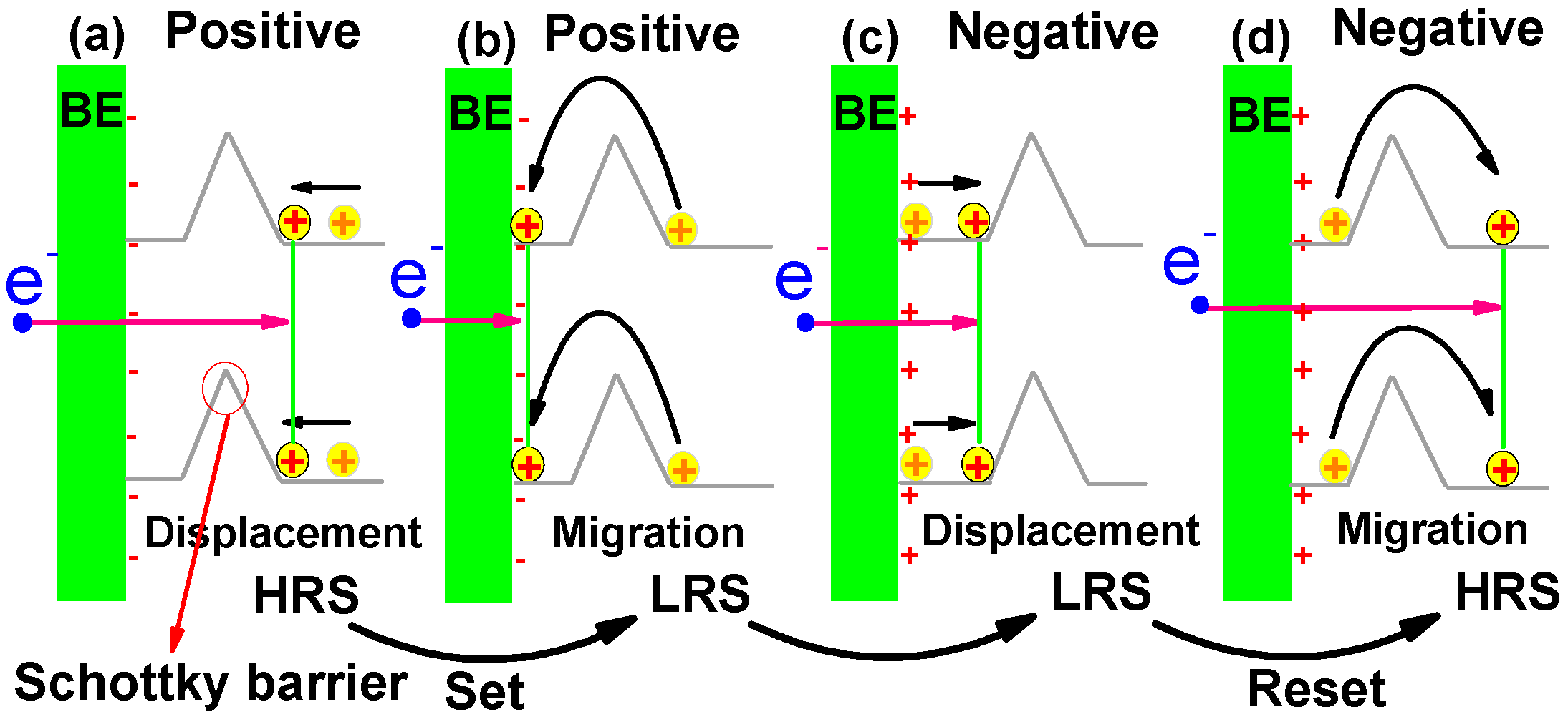
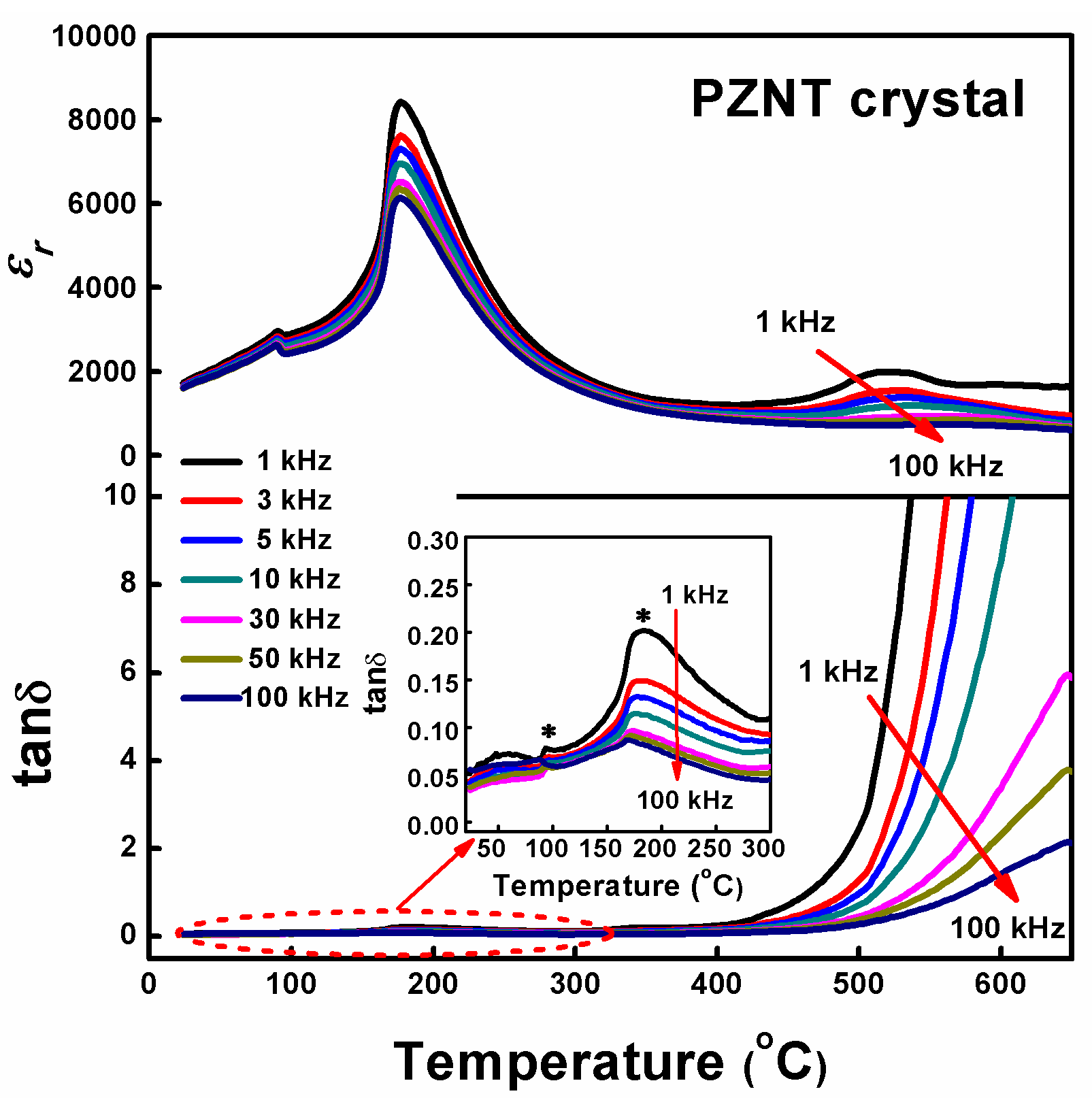
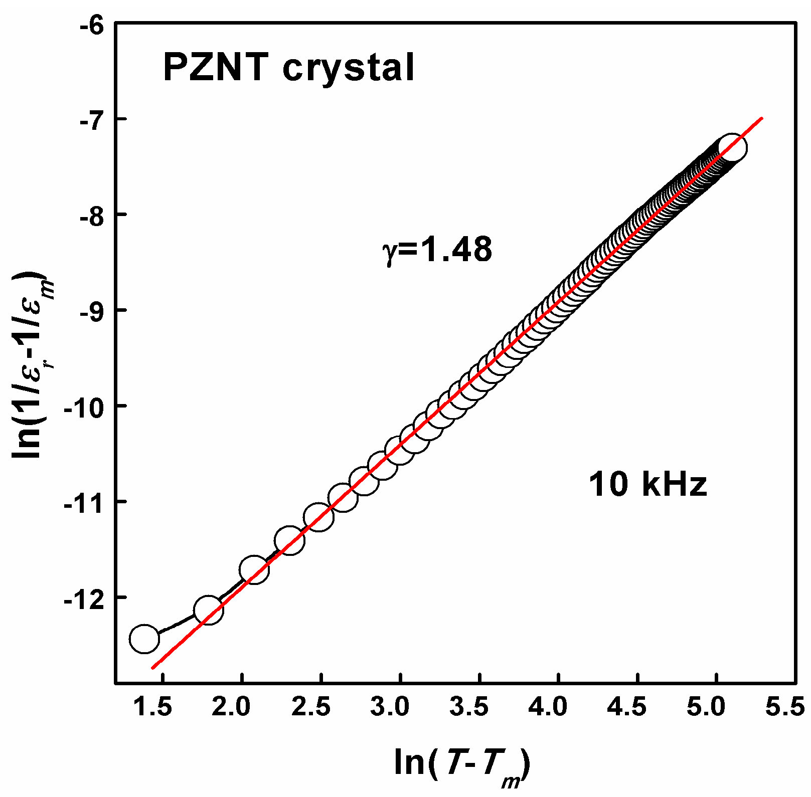
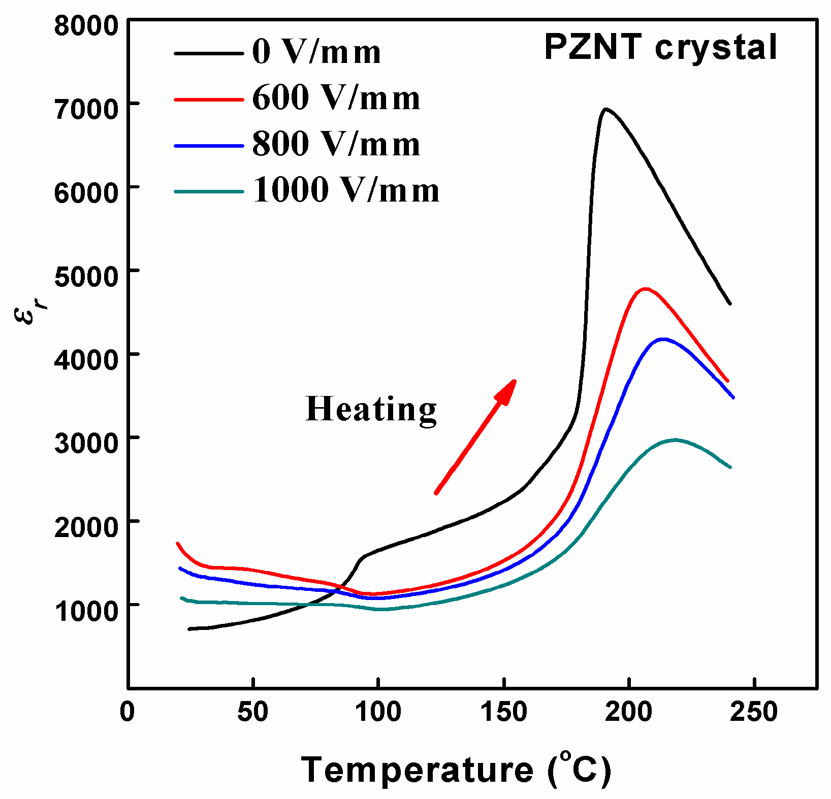
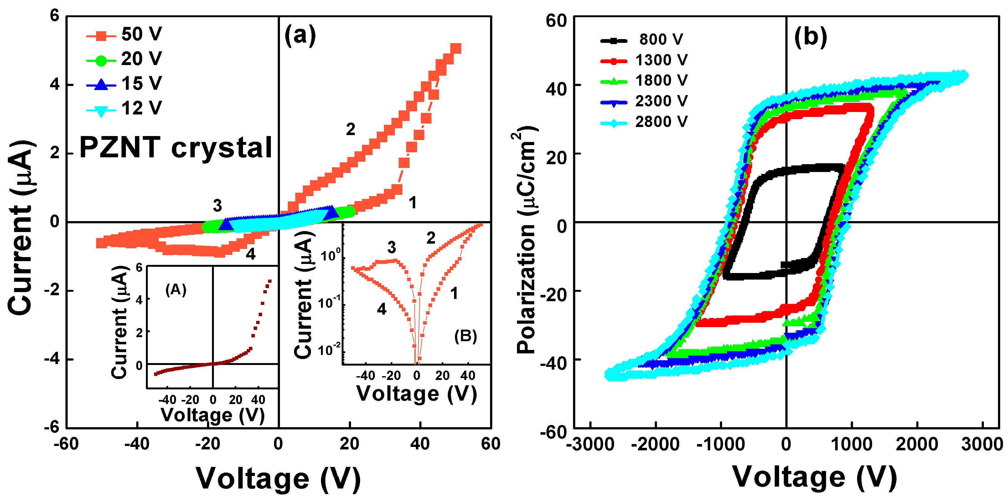
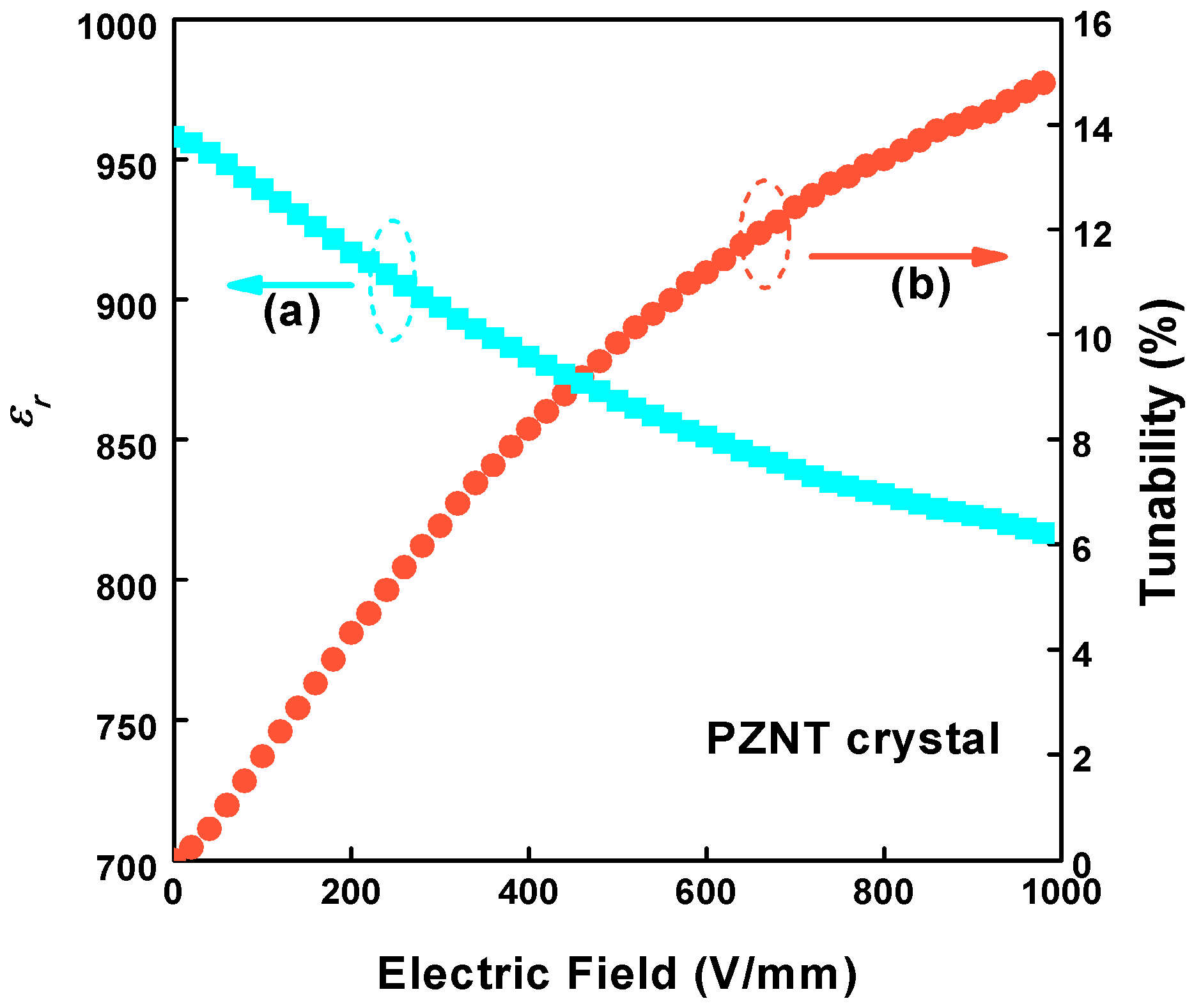
3. Results and Discussion

The current-voltage (IV) curves for the (100)-oriented PZNT single crystal obtained by decreasing the sweep range step by step are shown in Figure 1a. In the range of ±50 V, the test voltage was swept at a constant rate from 0–50 V, then to −50 V, before returning to 0 V. The numbers in the figure denote the sequence of the voltage sweeps. An asymmetry in the current can be observed in the figure. In addition, we can find that the IV curves show distinct hysteresis behavior, indicating the sample exhibited obvious resistance switching characteristics. Moreover, in the inset (A) of Figure 1a, the IV segment shows an obvious diode-like rectifying IV characteristic, indicating a diode behavior.
The IV curves plotted on semilogarithmic scales are shown in the inset (B) of Figure 1a. When the sweeping positive bias increased from 0 V to about 33.3 V, the resistance switching was in the high-resistance state (HRS), with a low current. When the voltage was beyond 33.3 V, the current increased quickly and attained a maximum (around 5 µA) with the voltage reached 50 V, indicating that the resistance switching “turns on” and switches from the HRS to the low-resistance state (LRS). As the voltage swept back from 50 V to about −33.3 V, the resistance switching remained in the LRS. As the resistance switching continued its negative bias, the current stabilized at around 0.7 µA until the sweeping bias exceeded −33.3 V, which led to a transition from the LRS to HRS. Finally, when the sweeping voltage returned, going from −50 to 0 V, the resistance switching remained in the HRS [34,35]. In addition, the resistance switching ratio was 229 at 2.08 V.
The mechanism of resistance switching characteristics is not yet perfectly understood. Despite this, there were some phenomenological models to explain these characteristics, namely the Schottky barrier model [36,37], space charge [38,39], the electrically conducting filamentary model [40,41], and the Mott transition [42]. Jeon et al. [43] reported that resistance switching characteristics are caused by the change in the Schottky potential based on the results from the first-principles calculations. It is worth mentioning that the observed ferroelectric resistance switching behavior in our crystal would be different from that observed in some ferroelectric tunneling junctions [44,45], because the tunneling current can only be taken into account for the ultrathin ferroelectric materials, not for our crystal with a thickness of 1 mm.
In the range of ±12, ±15 and ±20 V, the IV curve was almost symmetrical and without hysteresis, as shown in Figure 1a. Then, as the voltage increased to ±50 V, obvious hysteresis and resistance switching characteristics were observed. It was indicated that the current hysteresis and diode-like behavior can be triggered and switched at a high applied field. Figure 1b shows the P–E hysteresis loops for the PZNT single crystal with various voltages, indicating that the sample exhibits good ferroelectricity. It is worth mentioning that the P–E hysteresis loops starts at around ±45 V (not marked in the figure). According to the report of BiFeO3 [46], because the current and ferroelectric polarization exhibited the hysteresis phenomenon at a high applied field, the current hysteresis can be closely related to the ferroelectric polarization.
The polarization mechanism of ferroelectric materials includes displacement polarization and turning-direction polarization. In the process of the preparation of samples, lead vacancies will appear inevitably due to the volatility of lead, leading to the oxygen vacancies (OVs) due to charge neutrality restrictions. It is well known that the ionization of OVs will create conducting electrons in perovskite-structure oxides during the process of preparation at high temperatures, written as:
VoVo• + e'
Vo• → Vo•• + e'
where Vo•, Vo•• are single-ionized and double-ionized OVs, respectively. The current occurs by electron injection from one electrode affected by the concentration of OVs near the interface. So, according to the current study, we preferred to believe that the resistance switching characteristics of the PZNT single crystal could be caused by the change in the oxygen vacancies concentration at the metal/oxide interface by the electrically controlled electron injection.
In order to describe the processes underpinning resistance switching, the displacement and migration of OVs near the bottom electrode (BE) were introduced. Displacement was defined as the reversible movement of OVs under electrical bias (the OVs cannot get enough energy to go over the Schottky barrier), where upon removal of the applied voltage the OVs return to their initial locations. Migration occurred when the field-driven movement of the vacancies was not reversible upon removal of the bias (the OVs can get enough energy to go over the Schottky barrier) [47].
A model, shown in Figure 2a–d, was set up to explain the resistance switching characteristics of the PZNT single crystal. The yellow circles with plus signs in the model represented OVs. When the sweeping positive bias increased from 0 V to 33.3 V, the OVs could not get enough energy to go over the Schottky barrier. The positive bias displaces OVs towards BE (displacement of OVs) to enhance the electron injection, as shown in Figure 2a. However, when the bias was beyond 33.3 V, the OVs surmounted the Schottky barrier to BE (migration of OVs) because they obtained enough energy, and it greatly increased the electron injection, as shown in Figure 2b. Consequently, the current increased quickly, the resistance switching “turned on” and the switches changed their state from the HRS to the LRS. The state would remain until the bias reversal. As the voltage swept from 0 V to around −33.3 V, the state still remained at the LRS, but the current appeared asymmetric due to the displacement of OVs, as shown in Figure 2c. When the negative bias kept increasing, the resistance switching returned to the HRS because of the migration of the OVs. Finally, the resistance switching returned to the original state when the bias returned to 0 V.
In the heating temperature range from 20–650 °C at a rate of 2 °C min−1, the temperature dependence of the relative permittivity εr and the dielectric loss tanδ of the PZNT single crystal at various frequencies (from 1–100 kHz) are shown in Figure 3. The inset shows the dielectric loss tanδ in the temperature range between 20–300 °C. Permittivity curves for various frequencies exhibit organized (the relative permittivity εr decreased with the increasing frequency) and the dielectric peaks are located at the temperature of about 177 °C (temperature of the maximum dielectric permittivity (Tm)) and Tm is unchanged with the increasing frequency, indicating a phase transition from the FE phase to the PE cubic phase. Seung-Eek Park et al. reported that the phase transition temperature was 180 °C [25]. In the temperature of Tm, the values of the dielectric peak εm could be as high as 8420 at the measurement frequency of 1 kHz. With increasing the frequency from 1–100 kHz, the value of εm decreased from 8420 to 6135. Specially, there was another dielectric anomaly peak that took place at about 90 °C, indicating a phase transition from the FEr phase to the FEt phase. The same phenomenon had also been reported by Hosono et al. [48]. Obviously, we can observe (inset of Figure 3) the same phase transformation from the dielectric constant. However, it was worth noting that, at the high temperature range (400–650 °C), the permittivity curves presented a high-temperature relaxation phenomenon that looked like the behavior of a diffuse phase transition and the value of tanδ became large, because the space charge polarization or the conductivity of the insulating ceramics increased with the increase in temperature.
From Figure 3, the obvious frequency dispersion of the dielectric constant can be observed, and this phenomenon signifies the typical relaxer behavior of the present specimen. The dielectric characteristics of relaxor ferroelectric materials are well known to deviate from the typical Curie-Weiss behavior, and can be described by a modified Curie-Weiss relationship [49]:
1 / ε r 1 / ε m = ( T T m ) γ / C 1 , 1 γ 2
where γ and C1 are assumed to be constant. For γ = 1, a normal Curie-Weiss law was obtained, and a complete diffuse phase transition was described for γ = 2 [50]. The plots of ln(1/εr − 1/εm) versus ln(T − Tm) with a frequency of 10 kHz are shown in Figure 4. We can get the value of γ = 1.48 by fitting the experimental data. Values of γ in this work were found to vary from 1.31 to 1.62 in the frequency range from 1–300 kHz. This also supported the evidence of the relaxer nature of the PZNT single crystal.
At 100 Hz, the temperature dependence of εr for the PZNT single crystal during the heating process under different electric fields is shown in Figure 5. The curves of the temperature dependence of εr for the PZNT single crystal were lower and wider as the electric field increased, indicating that the single crystal went through a field-induced phase transition. When the value of the applied field was 0 kV/mm, the maximum relative permittivity (εm) was 6934 at about 190 °C and the εm decreased from 6934 to 2970 with the applied field increasing from 0 to 1 kV/mm. Particularly, the Tm presented a different value under different applied electric fields, suggesting that the single crystal underwent a second-order phase transition. The values of εm and Tm are listed in Table 1. The result clearly indicates a broadening of the dielectric peak due to the diffuse ferroelectric-paraelectric phase transition.
Dielectric tunable materials have a wide range of applications, such as in phase shifters, oscillators, filters, etc. [51]. From the above discussion, εr was found to be tunable by changing the electric field. The εr and the tunability of εr are shown in Figure 6, respectively. The test was conducted under different electric fields at 10 kHz at room temperature and the applied electric fields increased from 0 to 1000 V/mm. The tunability of εr is defined as [εr(0) − εr(E)] × 100%/εr(0), where εr(0) and εr(E) are the εr values when the electric field is zero and E, respectively. The results revealed that the largest tunability of εr was 14.78%. With the increase of the electric field, the εr decreased gradually and the tunability increased, respectively [52,53].
The pyroelectric coefficients as a function of the temperature for the PZNT single crystal are shown in Figure 7. The real part of the pyroelectric coefficients increases slowly from −576.1 to −447.4 μC/m2K with increasing temperatures from 18–50 °C, respectively. The imaginary part of the pyroelectric coefficients are pyroelectric losses. At a room temperature of 25 °C, the value of the pyroelectric coefficient was −463.3 μC/m2K, and the absolute value of the pyroelectric coefficient (463.3 μC/m2K) was higher than that of the graded PZT films on Pt-coated silicon substrates (202–250 μC/m2K) and Ba3Nb2O8 ceramic (103 μC/m2K) [32,54]. A useful comparative figure of merit (FOM) used in comparing pyroelectric materials is defined as FD = |P|/c(εrε0tanδ)1/2, where c is the heat capacity per unit volume (c = 2.5 J/cm3K) [55], εr is the relative permittivity, ε0 is the permittivity of the vacuum and tanδ is the dissipation factor. The FD value is 8.77 × 10⁻⁶ Pa−0.5 at 1 kHz. This result implies that the PZNT single crystal can be a promising material for pyroelectric array sensor applications.

4. Conclusions

In conclusion, this work has shown the resistance switching characteristics in the (100)-oriented PZNT single crystal. The current hysteresis can be closely related to the ferroelectric polarization and we provided a possible explanation with a model of oxygen vacancies to analyze the mechanism of switching. In the process of heating, the temperature of the rhombohedral-tetragonal phase transition was about 90 °C and the temperature of the FE-PE phase transition was about 177 °C. The obvious frequency dispersion of the relative permittivity signified the relaxer-type behavior of the sample, and the value of the relaxation parameter γ = 1.48, estimated from the linear fit of the modified Curie-Weiss law, indicated the relaxer nature. High-temperature dielectric relaxation behaviors were revealed in the temperature region of 400–650 °C. In addition, under the measuring frequency of 10 kHz, we found that εr was tunable by changing the electric field and the largest tunability of εr reached 14.78%. At room temperature, the pyroelectric coefficient and the figure of merit FD were −463.3 μC/m2 K and 8.77 × 10⁻⁶ Pa−0.5, respectively.

Acknowledgments

This work was supported by the National Natural Science Foundation of China (Grant Nos. 11574057 and 51604087), the Guangdong Provincial Natural Science Foundation of China (Grant No. 2016A030313718), the Science and Technology Program of Guangdong Province of China (Grant No. 2016A010104018) and the Youth Foundation of Guangdong University of Technology (Grant No. 14QNZA004).

Author Contributions

Xingui Tang conceived and designed the experiments. Xingui Tang and Zhi Zhu analyzed and interpreted the data and wrote the manuscript. All authors commented on the manuscript.

Conflicts of Interest

The authors declare no conflict of interest.

References

  1. Meijer, G.I. Materials science—Who wins the nonvolatile memory race? Science 2008, 319, 1625–1626. [Google Scholar] [CrossRef] [PubMed]
  2. Waser, R.; Aono, M. Nanoionics-based resistive switching memories. Nat. Mater. 2007, 6, 833–840. [Google Scholar] [CrossRef] [PubMed]
  3. Panda, D.; Huang, C.Y.; Tseng, T.Y. Resistive switching characteristics of nickel silicide layer embedded HfO2 film. Appl. Phys. Lett. 2012, 100, 112901. [Google Scholar] [CrossRef]
  4. Ghenzi, N.; Rozenberg, M.J.; Llopis, R.; Levy, P.; Hueso, L.E.; Stoliar, P. Tuning the resistive switching properties of TiO2-x films. Appl. Phys. Lett. 2015, 106, 123509. [Google Scholar] [CrossRef]
  5. Santhanakrishna, A.K.; Takshi, A. Photoelectric Memory Effect in an Organic Bulk Heterojunction Device. J. Phys. Chem. C 2015, 119, 17253–17259. [Google Scholar] [CrossRef]
  6. Li, J.C.; Hou, X.Y.; Cao, Q. Effect of Cu doping on the resistive switching of NiO thin films. J. Appl. Phys. 2014, 115, 164507. [Google Scholar] [CrossRef]
  7. Salomone, L.S.; Kasulin, A.; Carbonetto, S.H.; Garcia-Inza, M.A.; Redin, E.G.; Berbeglia, F.; Lipovetzky, J.; Faigón, A.; Campabadal, F. Radiation and bias switch-induced charge dynamics in Al2O3-based metal-oxide-semiconductor structures. J. Appl. Phys. 2014, 116, 174506. [Google Scholar] [CrossRef]
  8. Chen, Y.C.; Chung, Y.L.; Chen, B.T.; Chen, W.C.; Chen, J.S. Revelation on the Interrelated Mechanism of Polarity-Dependent and Multilevel Resistive Switching in TaOx-Based Memory Devices. J. Phys. Chem. C 2013, 117, 5758–5764. [Google Scholar] [CrossRef]
  9. Zhang, Y.; Deng, N.; Wu, H.; Yu, Z.; Zhang, J.; Qian, H. Metallic to hopping conduction transition in Ta2O5-x/TaOy resistive switching device. Appl. Phys. Lett. 2014, 105, 063508. [Google Scholar] [CrossRef]
  10. Huang, Z.C.; Chen, Q.; Zhai, Y.; Wang, J.L.; Xu, Y.B. Oxygen vacancy induced magnetization switching in Fe3O4 epitaxial ultrathin films on GaAs(100). Appl. Phys. Lett. 2015, 106, 182401. [Google Scholar] [CrossRef]
  11. Sim, H.J.; Choi, D.; Lee, D.; Seo, S.; Lee, M.-J.; Yoo, I.-K.; Hwang, H. Resistance-switching Characteristics of polycrystalline Nb2O5 for nonvolatile memory application. IEEE Electron. Dev. Lett. 2005, 26, 292–294. [Google Scholar]
  12. Kubicek, M.; Schmitt, R.; Messerschmitt, F.; Jennifer, L.M.R. Uncovering Two Competing Switching Mechanisms for Epitaxial and Ultrathin Strontium Titanate-Based Resistive Switching Bits. ACS Nano 2015, 9, 10737–10748. [Google Scholar] [CrossRef] [PubMed]
  13. Park, J.H.; Kwon, D.H.; Park, H.G.; Jung, C.U.; Kim, M. Role of oxygen vacancies in resistive switching in Pt/Nb-doped SrTiO3. Appl. Phys. Lett. 2014, 105, 183103. [Google Scholar] [CrossRef]
  14. Guo, Z.L.; Sa, B.S.; Zhou, J.; Sun, Z.M. Role of oxygen vacancies in the resistive switching of SrZrO3 for resistance random access memory. J. Alloy. Compd. 2013, 580, 148–151. [Google Scholar] [CrossRef]
  15. Seong, T.G.; Choi, K.B.; Seo, I.T.; Oh, J.H.; Moon, J.W.; Hong, K.; Nahm, S. Resistive switching properties of amorphous Pr0.7Ca0.3MnO3 films grown on indium tin oxide/glass substrate using pulsed laser deposition method. Appl. Phys. Lett. 2012, 100, 212111. [Google Scholar] [CrossRef]
  16. Sawa, A. Resistive switching in transition metal oxides. Mater. Today 2008, 11, 28–36. [Google Scholar] [CrossRef]
  17. Chen, X.; Tang, X.; Chen, X.-Z.; Chen, Y.-L.; Guo, X.; Ge, H.-X.; Shen, Q.-D. Nonvolatile data storage using mechanical force-induced polarization switching in ferroelectric polymer. Appl. Phys. Lett. 2015, 106, 042903. [Google Scholar] [CrossRef]
  18. Xie, Z.K.; Yue, Z.; Ruehl, G.; Peng, B.; Zhang, J.; Yu, Q.; Zhang, X.; Li, L. Bi(Ni1/2Zr1/2)O3-PbTiO3 relaxor-ferroelectric films for piezoelectric energy harvesting and electrostatic storage. Appl. Phys. Lett. 2014, 104, 243902. [Google Scholar] [CrossRef]
  19. Guo, E.J.; Herklotz, A.; Roth, R.; Christl, M.; Das, S.; Widdra, W.; Dörr, K. Tuning the switching time of BiFeO3 capacitors by electrodes’ conductivity. Appl. Phys. Lett. 2013, 103, 022905. [Google Scholar] [CrossRef]
  20. Yan, F.; Xing, G.Z.; Li, L. Low temperature dependent ferroelectric resistive switching in epitaxial BiFeO3 films. Appl. Phys. Lett. 2014, 104, 132904. [Google Scholar] [CrossRef]
  21. Zhang, L.X.; Chen, J.; Cao, J.L.; He, D.Y.; Xing, X.R. Large resistive switching and switchable photovoltaic response in ferroelectric doped BiFeO3-based thin films by chemical solution deposition. J. Mater. Chem. C 2015, 3, 4706–4712. [Google Scholar] [CrossRef]
  22. Zhao, B.Y.; Chen, Z.; Meng, J.; Lu, H.; Zhang, D.W.; Jiang, A. Ferroelectric polarization and defect-dipole switching in an epitaxial (111) BiFeO3 thin film. J. Appl. Phys. 2015, 117, 204103. [Google Scholar] [CrossRef]
  23. Zhao, Y.J.; Yin, Z.G.; Zhang, X.W.; Fu, Z.; Wu, J.L. Formation and local conduction of nanopits in BiFeO3 epitaxial films. J. Mater. Chem. C 2015, 3, 11250–11256. [Google Scholar] [CrossRef]
  24. Shuai, Y.; Ou, X.; Wu, C.; Zhang, W.; Zhou, S.; Bürger, D.; Reuther, H.; Slesazeck, S.; Mikolajick, T.; Helm, M.; et al. Substrate effect on the resistive switching in BiFeO3 thin films. J. Appl. Phys. 2012, 111, 07D906–07D908. [Google Scholar] [CrossRef]
  25. Park, S.E.; Shrout, T.R. Characteristics of relaxor-based piezoelectric single crystals for ultrasonic transducers. IEEE Trans. Ultrason. Ferroelectr. Freq. Control 1997, 44, 1140–1147. [Google Scholar] [CrossRef]
  26. Bertram, R.; Reck, G.; Uecker, R. Growth and correlation between composition and structure of (1 − x)Pb(Zn1/3Nb2/3)O3–xPbTiO3 crystals near the morphotropic phase boundary. J. Cryst. Growth 2003, 253, 212–220. [Google Scholar] [CrossRef]
  27. Fang, B.J.; Xu, H.Q.; He, T.H.; Luo, H.S.; Yin, Z.W. Growth mechanism and electrical properties of [Pb(Zn1/3Nb2/3)0.91Ti0.09]O3 single crystals by a modified Bridgman method. J. Crystal. Growth 2002, 244, 318–326. [Google Scholar] [CrossRef]
  28. Zhang, H. Polarization rotation and field induced phase transition in PZN-4.5%PT single crystal. J. Appl. Phys. 2013, 114, 084109. [Google Scholar] [CrossRef]
  29. Zhang, H. Polarization rotation and phase transition in [100]-oriented PZN-PT single crystals determined by the electro-crystalline anisotropy. J. Appl. Phys. 2013, 114, 184102. [Google Scholar] [CrossRef]
  30. Bao, P.; Yan, F.; Dai, Y.; Zhu, J.; Wang, Y.; Luo, H. Dielectric relaxation in 91%Pb(Zn1/3Nb2/3)O3–9%PbTiO3 single crystal at low temperature. Appl. Phys. Lett. 2004, 84, 5317–5319. [Google Scholar] [CrossRef]
  31. Pilch, M.; Molak, A. Resistivity switching induced in ferroelectric phase of PbTiO3 studied by XPS and electric conductivity tests. J. Alloy. Compd. 2014, 586, 488–498. [Google Scholar] [CrossRef]
  32. Tang, X.G.; Jiang, L.L.; Kuang, S.J.; Ding, A.L.; Chan, H.L.W. Dielectric and pyroelectric properties of compositionally graded Pb(Zr1-xTix)O3 thin films prepared by sol-gel process. Chin. J. Chem. Phys. 2007, 20, 665–669. [Google Scholar] [CrossRef]
  33. Tang, X.G.; Chan, H.L.W.; Ding, A.L. Electrical properties of compositionally graded lead calcium titanate thin films. Solid State Commun. 2003, 127, 625–628. [Google Scholar] [CrossRef]
  34. Wouters, D.J.; Waser, R.; Wuttig, M. Phase-Change and Redox-Based Resistive Switching Memories. Proc. IEEE 2015, 103, 1274–1288. [Google Scholar] [CrossRef]
  35. Qiu, J.; Shih, A.; Zhou, W.D.; Mi, Z.T.; Shih, I. Effects of metal contacts and dopants on the performance of ZnO-based memristive devices. J. Appl. Phys. 2011, 110, 014513. [Google Scholar] [CrossRef]
  36. Fujii, T.; Kawasaki, M.; Sawa, A.; Akoh, H.; Kawazoe, Y.; Tokura, Y. Hysteretic Current-Voltage Characteristics and Resistance Switching at an Epitaxial Oxide Schottky Junction SrRuO3/SrTi0.99Nb0.01O3. Appl. Phys. Lett. 2005, 86, 012107. [Google Scholar] [CrossRef]
  37. Sawa, A.; Fujii, T.; Kawasaki, M.; Tokura, Y. Hysteretic Current-Voltage Characteristics and Resistance Switching at a Rectifying Ti/Pr0.7Ca0.3MnO3 Interface. Appl. Phys. Lett. 2004, 85, 4073–4075. [Google Scholar] [CrossRef]
  38. Lee, M.H.; Kim, K.M.; Kim, G.H.; Seok, J.Y.; Song, S.J.; Yoon, J.H.; Hwang, C.S. Study on the Electrical Conduction Mechanism of Bipolar Resistive Switching TiO2 Thin Films Using Impedance Spectroscopy. Appl. Phys. Lett. 2010, 96, 152909. [Google Scholar] [CrossRef]
  39. Shang, D.S.; Wang, Q.; Chen, L.D.; Dong, R.; Li, X.M.; Zhang, W.Q. Effect of Carrier Trapping on the Hysteretic Current–Voltage Characteristics in Ag/La0.7Ca0.3MnO3/Pt Heterostructures. Phys. Rev. B 2006, 73, 245427. [Google Scholar] [CrossRef]
  40. Kim, D.C.; Seo, S.; Ahn, S.E.; Suh, D.-S.; Lee, M.J.; Park, B.-H.; Yoo, I.K.; Baek, I.G.; Kim, H.-J.; Yim, E.K.; et al. Electrical Observations of Filamentary Conductions for the Resistive Memory Switching in NiO Films. Appl. Phys. Lett. 2006, 88, 202102. [Google Scholar] [CrossRef]
  41. Rohde, C.; Choi, B.J.; Jeong, D.S.; Choi, S.; Zhao, J.-S.; Hwang, C.S. Identification of a Determining Parameter for Resistive Switching of TiO2 Thin Films. Appl. Phys. Lett. 2005, 86, 262907. [Google Scholar] [CrossRef]
  42. Fujimoto, M.; Koyama, H.; Konagai, M.; Hosoi, Y.; Ishihara, K.; Ohnishi, S.; Awaya, N. TiO2 Anatase Nanolayer on TiN Thin Film Exhibiting High- Speed Bipolar Resistive Switching. Appl. Phys. Lett. 2006, 89, 223509. [Google Scholar] [CrossRef]
  43. Jeon, S.H.; Park, B.H.; Lee, J.; Lee, B.; Han, S. First-principles Modeling of Resistance Switching in Perovskite Oxide Material. Appl. Phys. Lett. 2006, 89, 042904. [Google Scholar] [CrossRef]
  44. Maksymovych, P.; Jesse, S.; Yu, P.; Ramesh, R.; Baddorf, A.P.; Kalinin, S.V. Polarization Control of Electron Tunneling into Ferroelectric Surfaces. Science 2009, 324, 1421–1425. [Google Scholar] [CrossRef] [PubMed]
  45. Garcia, V.; Fusil, S.; Bouzehouane, K.; Enouz-Vedrenne, S.; Mathur, N.D.; Barthelemy, A.; Bibes, M. Giant tunnel electroresistance for non-destructive readout of ferroelectric states. Nature 2009, 460, 81–84. [Google Scholar] [CrossRef] [PubMed]
  46. Wang, C.; Jin, K.J.; Xu, Z.T.; Wang, L.; Ge, C.; Lu, H.B.; Guo, H.Z.; He, M.; Yang, G.Z. Switchable diode effect and ferroelectric resistive switching in epitaxial BiFeO3 thin films. Appl. Phys. Lett. 2011, 98, 192901. [Google Scholar] [CrossRef]
  47. Mojarad, S.A.; Goss, J.P.; Kwa, K.S.K.; Zhou, Z.Y.; Al-Hamadany, R.A.S.; Appleby, D.J.R.; Ponon, N.K.; O’Neill, A. Leakage current asymmetry and resistive switching behavior of SrTiO3. Appl. Phys. Lett. 2012, 101, 173507. [Google Scholar] [CrossRef]
  48. Hosono, Y.; Harada, K.; Kobayashi, T.; Itsumi, K.; Izumi, M.; Yamashita, Y.; Ichinose, N. Temperature dependence of dielectric and piezoelectric properties of Pb(Zn1/3Nb2/3)O3-PbTiO3 piezoelectric single crystals. Jpn. J. Appl. Phys. 2002, 41, 7084–7088. [Google Scholar] [CrossRef]
  49. Zhang, T.F.; Tang, X.G.; Huang, X.X.; Liu, Q.X.; Jiang, Y.P.; Zhou, Q.F. High-Temperature Dielectric Relaxation Behaviors of Relaxer-Like PbZrO3-SrTiO3 Ceramics for Energy-Storage Applications. Energy Technol. 2016, 4, 633–640. [Google Scholar] [CrossRef]
  50. Zhang, J.J.; Zhai, J.W.; Zhang, Y.W. Microwave and infrared dielectric response in BaTiO3 based relaxor ferroelectrics. Phys. Status Solidi A 2011, 208, 2853–2860. [Google Scholar] [CrossRef]
  51. Chou, X.J.; Zhai, J.W.; Yao, X. Dielectric tunable properties of low dielectric constant Ba0.5Sr0.5TiO3-Mg2TiO4 microwave composite ceramics. Appl. Phys. Lett. 2007, 91, 122903–122908. [Google Scholar] [CrossRef]
  52. Feng, Z.Y.; Zhao, X.Y.; Luo, H.S. Composition and orientation dependence of phase configuration and dielectric constant tunability in poled Pb(Mg1/3Nb2/3)O3-PbTiO3 single crystal. J. Phys. Condens. Matter 2004, 16, 6771–6778. [Google Scholar] [CrossRef]
  53. Tang, X.G.; Chew, K.-H.; Chan, H.L.W. Diffuse phase transition and dielectric tunability of Ba(ZryTi1-y)O3 relaxor ferroelectric ceramics. Acta Mater. 2004, 52, 5177–5183. [Google Scholar] [CrossRef]
  54. Pati, B.; Choudhary, R.N.P.; Das, P.R.; Parida, B.N.; Padhee, R. Pyroelectric and dielectric properties of lead-free ferroelectric Ba3Nb2O8 ceramic. J. Alloy. Compd. 2014, 592, 6–11. [Google Scholar] [CrossRef]
  55. Whatmore, W.R.; Patel, A.; Shorrock, N.M.; Ainger, F.W. Ferroelectric materials for thermal ir sensors state-of-the-art and perspectives. Ferroelectrics 1990, 104, 269–283. [Google Scholar] [CrossRef]
Figure 1. (a) The IV curves for the PZNT single crystal by decreasing the sweep range step by step; Inset (A) shows the obvious diode-like rectifying IV characteristic, indicating a diode behavior; Inset (B) shows the IV curves plotted on semilogarithmic scales; (b) The PE hysteresis loops for the PZNT single crystal with various voltages.
Materials 10 00349 g001
Figure 2. The displacement of OVs (a) and migration of OVs (b) under positive bias to enhance the electron injection; The displacement of OVs (c) and migration of OVs (d) under negative bias to reduce the electron injection.
Materials 10 00349 g002
Figure 3. The relative permittivity εr and dielectric loss tanδ as a function of temperature for the PZNT single crystal measured at different frequencies. The inset shows the dielectric loss tanδ in the temperature range between 20–300 °C
Materials 10 00349 g003
Figure 4. Plot of ln(1/εr 1/εm) as a function of ln(TTm) for the PZNT single crystal measured at 10 kHz.
Materials 10 00349 g004
Figure 5. Temperature dependence of the relative permittivity (εr) of the PZNT single crystal under various electric fields at 100 Hz.
Materials 10 00349 g005
Figure 6. At room temperature, 10 kHz of AC bias and composition dependence of (a) the relative permittivity εr; (b) the tunability of εr of the PZNT single crystal.
Materials 10 00349 g006
Figure 7. The pyroelectric coefficient as a function of temperatures for the PZNT single crystal.
Materials 10 00349 g007
Table 1. The maximum relative permittivity and corresponding temperature under different electric fields.
Electric Field (V/mm)06008001000
εm6934477941792970
Tm (°C)190206214218

