Germanium Based Field-Effect Transistors: Challenges and Opportunities

Abstract
: The performance of strained silicon (Si) as the channel material for today’s metal-oxide-semiconductor field-effect transistors may be reaching a plateau. New channel materials with high carrier mobility are being investigated as alternatives and have the potential to unlock an era of ultra-low-power and high-speed microelectronic devices. Chief among these new materials is germanium (Ge). This work reviews the two major remaining challenges that Ge based devices must overcome if they are to replace Si as the channel material, namely, heterogeneous integration of Ge on Si substrates, and developing a suitable gate stack. Next, Ge is compared to compound III-V materials in terms of p-channel device performance to review how it became the first choice for PMOS devices. Different Ge device architectures, including surface channel and quantum well configurations, are reviewed. Finally, state-of-the-art Ge device results and future prospects are also discussed.1. Introduction
The motivation to replace strained silicon (Si) with higher mobility channel materials in today’s metal-oxide-semiconductor field-effect transistors (MOSFETs) is well documented [1,2]. Saturation drive current (Ion), a critical performance metric for FET devices, is intimately linked with carrier mobility. While this link has become less clear as devices are scaled down into quasi-ballistic and ballistic regimes, the general relation continues to hold [3]. In light of this relationship, future transistor scaling will require the introduction of new high mobility channel materials, including germanium (Ge) or III-V semiconductors. The higher carrier mobility offered by these materials compared to strained silicon presents a practical means to push Ion higher, even at lower supply voltages. On the other hand, even with the change in device architecture from planar to F in FET, continued scaling of today’s Si transistors is expected to provide only a few additional generations of technology. As seen in Figure 1, the hole mobility enhancement as a function of strain is much flatter in Si than for Ge. This suggests that if the challenges associated with Ge channel transistors can be overcome, the technology may continue to be scalable for decades.
The effort to move to higher mobility channel materials is complicated by the fact that it must, in a sense, be done twice, once for n-channel FETs (NMOS) and once for p-channel FETs (PMOS). The nature of complementary MOS logic (CMOS) requires comparably performing NMOS and PMOS devices working in tandem. Historically, NMOS transistors have outperformed PMOS since electron mobility (μe) is generally significantly higher than hole mobility (μh). Circuit designers have adapted to working with PMOS devices with about one third the performance of NMOS, so preferably the performance gap in the next generation of technology should be no larger than this [1]. Additionally, it is strongly favorable to use the same material system for both n-channel and p-channel devices (either Ge for both, or for example, InGaAs for both) since this substantially simplifies device processing [4,5]. Due to the exceptionally high μh of Ge, and the progress made in Ge based p-channel MOSFETs (pMOSFETs) [6–14] and p-channel quantum well FETs (pQWFETs) [2,15–19] over the last decade, there appears to be a consensus in the device research community and in industry that Ge offers the best option for PMOS devices [1,2,20]. In light of this, there is heightened incentive to develop Ge based NMOS devices that perform comparably. There are, however, significant additional engineering challenges to achieving this, such as overcoming Ge’s tendency for have a higher interface state density (Dit) near the conduction band edge [21,22] and developing low resistance ohmic contacts to n-type Ge [23,24].
High mobility III-V materials present an alternative to Ge for future CMOS technology nodes. In III-V material systems, experimental outcomes have been the inverse of that seen with Ge—i.e., excellent III-V based NMOS devices have been demonstrated [25,26], whereas a comparably performing PMOS device using the same channel material is still elusive to date [1]. This is in large part due to the significant disparity in electron and hole mobility in III-V materials; with μe typically being at least several times larger than μh [1]. For this reason, it is not unlikely that a future CMOS technology node will involve co-integration of Ge based PMOS and III-V based NMOS devices together. Unfortunately, such a path would also entail finding ways to deal with the increased processing complexity that comes with having multiple material systems with different chemistries and thermodynamic stability on the same chip.
The above discussion has led to a choice of two paths, the dual-Ge path (for both NMOS and PMOS) or the III-V/Ge path (NMOS/PMOS). To be sure, there is also a possibility of a dual-III-V path; or it may be found the performance benefit of Ge and III-V over strained silicon (which is itself a moving target) fails to justify the increase in complexity and cost. The former seems the least likely of all alternatives, and the latter falls outside the scope of the present article. This review first summarizes the two major challenges that must be overcome to succeed in either path involving Ge: heterogeneous integration of Ge on Si, and developing a suitable gate stack. After this, a major challenge to the dual-Ge path, achieving low resistance ohmic contacts on n-type Ge, is briefly discussed. The basis for Ge’s selection over III-V for PMOS is also summarized. Finally, Ge device architectures and state-of-the-art results are reviewed. Many excellent review articles already exist for Ge based devices, with most focusing on the MOSFET architecture [2,11,27–30]. This review article presents recent advancements in the field of Ge based nanoscale MOSFETs and QWFETs.
2. Challenges
2.1. Heterogeneous Integration on Silicon
Due to low economic availability, any long-term widespread utilization of Ge for electronic device applications will almost certainly be in the form of thin epitaxial films grown on cheaper and more abundant Si substrates. Integration on Si is doubly important due to the expectation that other Si components, such DRAM and non-volatile memory, will be included on the same chips [31]. As a consequence, perhaps the most significant hurdle to the widespread adoption of Ge in devices is the lattice mismatch with respect to Si. This problem is further aggravated by the thermal expansion coefficient mismatch in these two materials. Lattice mismatch is defined as:
where ae is the lattice parameter of the epitaxial layer and as is that of the substrate material. The lattice mismatch leads to a large buildup of strain energy in Ge layers epitaxially grown on Si. This strain energy is primarily relieved by two mechanisms: (i) generation of lattice dislocations at the interface (misfit dislocations) and (ii) elastic deformation of both the substrate and the Ge islands which form on the surface during early stages of growth (following the Stranski-Krastanow growth mode) [32]. In general, elastic deformation cannot accommodate all the strain and as a result, misfit dislocations nucleate at the island edges [33]. Many dislocations bend toward the growth direction and propagate, or thread, to the surface during growth. These threading dislocations severely degrade carrier transport properties by lowering carrier mobility and decreasing carrier lifetime. This dilemma necessitates the development of means to more gracefully bridge the lattice constants of the two materials. To accomplish this, several buffer architectures have been proposed and experimentally demonstrated. These approaches are summarized in Table 1. While not complete, Table 1 does highlight the wide variety of methods that have been explored for Ge on Si heteroepitaxy. Thinner buffers are generally preferred to reduce cost and facilitate heat dissipation. For FET applications, the buffer should be comprised of wide bandgap materials to (i) provide device isolation and (ii) suppress parallel conduction—two phenomena discussed in more detail later. A good buffer is further characterized by a low threading dislocation density (TDD) and low root-mean-square (RMS) roughness at the surface so that it may serve as a smooth template for active layer growth. It is believed that for device quality growth, a starting surface with a TDD of 106 cm−2 or less, and a RMS roughness of 1 nm or less, is required. The approaches summarized in Table 1 generally fall into five categories: (i) direct epitaxy of Ge on Si, (ii) growing layers of Si1–xGex where x is graded from zero to one, (iii) surfactant mediated epitaxy (SME), (iv) aspect ratio trapping (ART), and (v) the oxide buffer. Each of these architectures is briefly reviewed in the following sections. It should be pointed out that buffer architectures demonstrating heterogeneous integration of GaAs on Si may also prove useful for Ge. This is due to the close lattice match between GaAs and Ge (0.07%), which significantly reduces the complexity of Ge on GaAs growth [34]. An excellent review of GaAs on Si epitaxy can be found in [35]. The higher bandgap of GaAs (1.42 eV) compared to Ge (0.67 eV) suggests that GaAs-based buffers should exhibit less parallel conduction than Ge-based ones. One exciting GaAs/Si work been added to Table 1 [25].
2.1.1. Direct Epitaxy
The direct epitaxy approach is attractive due to its relative simplicity, and with the aid of high temperature hydrogen annealing, this method has demonstrated films with low RMS surface roughness (less than 1 nm) [38]. In regards to defect density however, direct epitaxy methods have had mixed results [47]. This method often involves a two-step low temperature then high temperature (LT/HT) Ge growth process. First a low temperature, low growth rate “seed” layer is grown which is intended to confine most of the defects. Together with Ge’s low surface diffusivity, lowering the growth temperature tends to prevent the impinging Ge from forming islands on the surface, resulting in flatter and more homogenous coverage of the Si substrate. After approximately 30 nm of growth the strain in the Ge surface will be fully relaxed due to the generation of misfit dislocations [48]. After the low temperature layer, a high temperature and high growth rate layer is deposited and is expected to be of higher crystalline quality since (i) the higher growth temperature annihilates defects and dislocations associated with strain relaxation, and (ii) the Ge is growing on a fully relaxed Ge “seed” layer instead of Si.
Separately from the two-step LT/HT approach, Nayfeh et al. [37] clearly demonstrated the benefit of hydrogen annealing of Ge layers on Si. The group reported an 88% reduction in RMS roughness for a 200 nm thick Ge layer grown on Si (at 400 °C) that was annealed for 1 hour at 825 °C in H2, compared to no reduction for a sample annealed in N2. They attributed the improved flatness to the increased surface mobility of the Ge-H cluster compared to Ge alone. Interestingly, the group found the ratio of optimal annealing temperatures for Si and Ge (1423 K/1073 K = 1.326) to be nearly equal to the ratio of their melting points (1687 K/1211 K = 1.393). In a separate paper [36] the same group used this approach to fabricate a Ge pMOSFET. They have grown a second Ge layer (400 °C, 250 nm thick) on top of a Ge layer produced by the method described in their previous work [37]. The resulting structure is shown in Figure 2. They observed a 2× increase in effective low-field mobility and a 3× increase in effective high-field mobility in a fabricated Ge pMOSFET compared to Si. Recently, this Ge on Si growth method was used in combination with a patterned SiO2 mask to achieve selective-area growth of Ge on Si and obtained a TDD of 1 × 107 cm−2 and RMS roughness of 0.61 nm [49]. Hartmann et al. [50] reported a Ge surface with a TDD of 6 × 106 cm−2 and RMS roughness of ~1 nm. The group used a similar two-step LT/HT growth process (400 °C/750 °C) and the total buffer thickness was 2.5 μm. Following growth, the structure was cyclically annealed (eight times 750 °C−10 min/900 °C−10 min) in H2. The hydrogen annealing was found to be critical for minimizing TDD, lowering it by nearly one order of magnitude (from ~4 × 10⁷ to 6 × 106 cm−2), but at the cost of a small increase in RMS roughness (increasing it from ~0.7 to ~1.1 nm). It should be noted that the group has assumed TDD to be equal to pit density measured by atomic force microscopy (AFM). Kobayashi et al. [51] observed more than one order of magnitude difference between the TDD measured by plan-view transmission electron microscopy (TEM) and the pit density measured by AFM. Choi et al. [38] have grown multiple two-step LT/HT dual layer stacks and have used 30 min hydrogen annealing at 800 °C between each set. They found the AFM pit density reduced by 80% between the first and second sets of LT/HT layers. After three sets of growth and H2 annealing (and a total Ge thickness of ~1.81 μm) they achieved a TDD measured by plan-view TEM of 0.8–1 × 107 cm−2 and RMS roughness of 0.4–0.6 nm. This is encouraging since additional sets of LT/HT growth and annealing could result in even lower TDD and RMS roughness, albeit with decreasing gains and additional buffer thickness.
Having a buffer composed of high bandgap material helps ensure that performance characteristics of a given device in an array are as much as possible independent of the on/off states of adjacent devices, or that is it electrically isolated from them. A pure Ge based buffer directly on Si would be expected to have poor device isolation characteristics due to the low bandgap of Ge. This alone is not necessarily mark against the direct epitaxy approach since it could be combined with commercially available silicon-on-insulator (SOI) substrates to improve device isolation, although this would also require that the buffer be quite thin to facilitate etching down to the buried oxide. A more serious concern for this approach is the prospect of parallel conduction of current through the buffer between the source and drain. An excellent review on the nature of parallel conduction can be found in [52]. The existence of additional higher conductivity paths between the source and drain, such as that provided by low bandgap buffer layers, has two primary consequences. First, it provides the means for a higher off-state current in FET devices, which in turn reduces the Ion/Ioff ratio and contributes power losses. This is exacerbated by the fact that the conductivity of these secondary paths is not effectively modulated by the gate voltage. Second, it undermines the device’s ability to confine carriers to the layer or path of highest mobility, which is particularly important in QWFET applications (discussed in section three). Failure to confine carriers to the highest mobility layer decreases on-state current, which also further reduces the device Ion/Ioff ratio. More investigation is needed to determine if parallel conduction is serious issue for the direct epitaxy approach.
2.1.2. The Graded Si1–xGex Buffer
The graded SixGe1–x buffer approach aims to introduce the 4.2% lattice mismatch gradually rather than abruptly as in the direct epitaxy approach. This is possible since the lattice mismatch of Si1–xGex on Si is roughly proportional to the Ge composition (x). Furthermore, the threading dislocations created during growth of the initial low-Ge composition layers can be preserved and reused to relieve additional strain generated in subsequent higher-Ge composition layers by carefully controlling the grading rate and the growth temperature. The gliding of existing threading dislocations suppresses nucleation of additional dislocations. A notable implementation of this approach was carried out by Currie et al. [40]. The group achieved a remarkable TDD of 2.1 × 106 cm−2. However, the total buffer thickness was 12 μm and the RMS roughness was 24.2 nm. Additionally, the group introduced a chemical-mechanical-polish (CMP) step near the growth midpoint since it was observed that the dislocations had a tendency to pile-up and become trapped, and therefore unable to continue to facilitate strain relief in subsequent layers. Samples with this added CMP step showed lower TDD of ~2.1 × 106 cm−2 and lower RMS roughness of 24.2 nm (compared to 1–5 × 107 cm−2 and 47 nm without the CMP). Loh et al. [53] later combined the graded SiGe buffer approach and the LT/HT approach to obtain an estimated TDD of 6 × 106 cm−2 (estimated by etch pit density) and RMS roughness of 1.4 nm using a buffer of only about 160 nm.
To help address the concern of device isolation, the graded SiGe buffer approach could be carried out on silicon on insulator (SOI) substrates, as shown by the Loh group [53]. As with the direct epitaxy approach, more experiments are need to investigate to nuisance of parallel conduction.
2.1.3. Surfactant Mediated Epitaxy (SME)
The amount of strain in epitaxial layers strongly influences the growth mode of the film. In the case of Ge on Si, the growth is flat (2D) for the first few monolayers. As the built-in strain energy increases with increasing film thickness, there is a sudden transition from 2D to 3D growth modes, also known as island growth [33]. It has been shown that this 2D-to-3D growth mode transition can be suppressed by deliberate introduction of a surfactant to alter the surface free energy, resulting in smoother layer-by-layer growth [54].
The general procedure for SME is as follows. The Si substrate is first capped with ~1 ML of the surfactant. The first surfactant investigated for Ge/Si growth was As. The extra valence electron from the As in the capping layer fills the dangling bonds at the Si surface, resulting in a stable, or energetically favorable termination. Following capping layer deposition, Ge growth begins. Surface termination with As remains energetically favorable since the Ge surface also contains dangling bonds. As a result, Ge atoms on the surface efficiently exchange sites with As in the capping layer. By this process the As capping layer “floats” on the surface even as Ge atoms continue to impinge on the surface, and the surface mobility of the growing species is strongly diminished, effectively suppressing the ability of the Ge to form islands. A drawback of the SME approach is that some of the surfactant inevitably incorporates into the film bulk, leading to a moderate (1016–1019 cm−3) n-type background doping.
In thicker films where islanding occurs, many defects thread towards the surface where the islands eventually coalesce. Using a surfactant to preserve the 2D growth mode also alters the defect structure that forms to relieve the lattice strain. LeGoues et al. [33] found that when As is used as the surfactant during Ge on Si(100) growth it results in V-shaped defects that can generate stacking faults and twins that extend throughout the entire film. Horn-von Hoegen et al. [55] showed that when Sb is used as the surfactant for Ge/Si(111) heteroepitaxy the threading defects generated to relieve stain during initial stages later self-annihilate as growth proceeds. This results in a network of dislocations confined at the Ge/Si(111) interface, and comparatively much fewer defects in the bulk of the film. A TDD of less than 108 cm−2 and background doping of 3–4 × 1019 cm−3 were estimated. More recently, Wietler et al. [41] used Sb for Ge on Si(100) growth to achieve fully relaxed Ge layers with a TDD of 1.6 × 108 cm−2 measured by plain-view TEM. The group used a relatively high substrate growth temperature of 670 °C and Sb flux of 2.4 ML/min. The high temperature helped facilitate Sb segregation to the surface, leading to a relatively low background doping of 3–4 × 1016 cm−3 in the Ge film. To further address the issue of surfactant incorporation in the Ge layer, it has recently been proposed to use carbon as the surfactant in place of Sb since carbon in Ge (i) does not act as a dopant and (ii) has very low solid solubility [56,57].
2.1.4. Aspect Ratio Trapping (ART)
The ART approach, also called “epitaxial necking” [58], for Ge-on-Si heteroepitaxy is built on the premise that most threading dislocations do not run normal to the Ge/Si interface. Therefore, by growing Ge on Si within narrow trenches formed by patterned oxide, dislocations angled away from the normal are likely to eventually collide with and become “trapped” by the trench sidewall.
ART begins by thermally growing 0.5–1 μm of oxide on the substrate. Trenches are formed in the oxide using standard lithography and reactive ion etching (RIE). Bai et al. [59] developed a model to determine the optimal dimensions, or aspect ratio (AR=height/width), of the trenches. Park et al. [60] showed that trenches with AR > 1 were needed to effectively trap defects within the sidewalls. A drawback of ART growth is that, while the length of trenches is arbitrary, the width of the area available for Ge devices is restricted to less than 1 μm by the AR > 1 requirement and the need for relatively thin buffers. To obtain a larger area of high-quality Ge for device growth, the Ge can be overgrown beyond the trench height, resulting in epitaxial lateral overgrowth (ELO). However, when ELO emerging from adjacent trenches coalesces, it forms new defects, as shown in Figure 3c(3). Defects originating at the Ge/Si interface in the trench (1) do not appear to propagate beyond the trench height (2). To avoid the defects formed by ELO coalescence, Park et al. [42] later used a growth process optimized for lateral growth, and CMP, to develop long 20 μm wide regions of Ge, grown from a single trench, with a TDD of 1.6 × 106 cm−3, shown in Figure 3a,b. For some device applications long 20 μm wide patches of high quality Ge may be sufficient [61]. If device area continues to improve, ART may become a viable method for creating Ge/Si virtual substrates for future high-performance Ge CMOS devices.
2.1.5. The Oxide Buffer
Two distinctly different oxide-based approaches have emerged for heterogeneous integration of Ge on Si: (i) the epitaxial oxide buffer [46,62–64], and (ii) heteroepitaxial growth of Ge on high Ge content SiGe-on-insulator (SGOI) substrates [43,65–67].
The epitaxial oxide based buffers are especially appealing due to (i) device isolation and (ii) the natural suppression of parallel conduction being inherently built-in to the structure. However, there is limited literature available on this method and more experiments are needed to clearly demonstrate its merit. Bojarczuk et al. [64] obtained a single-crystalline fully-relaxed layer (4 nm) of Ge on a (LaxY1–x)2O3/Si(111) template. Amorphous Ge was deposited on the crystalline (LaxY1–x)2O3 and subsequently heated to 450 °C under an Sb flux to induce an amorphous to crystalline transformation of the Ge. The Sb flux was found to reduce surface roughening during recrystallization. The quality of the Ge surface, in terms of RMS roughness and TDD, was not reported. Seo et al. [46] used a two stage SrHfxTi1–xO3 buffer on Si(100) to obtain a continuous and flat epitaxial Ge film, shown in Figure 4. The group conveyed that the method needed improvement due to low Hall-mobility (100–300 cm2/Vs) and a high density of stacking faults and twin structures (109 cm−2). Giussani et al. [63] used PrO2/Si(111) as a template for Ge(111) epitaxy and obtained a smooth single-crystalline Ge layer. However, an extended Ge deposition time was needed. Quantitative measurements of the surface quality were not provided.
The second oxide based approach, Ge on high Ge content SGOI substrates, is relatively new but has produced encouraging results. The method usually involves using the Ge condensation technique, proposed by Tezuka et al. [67], to convert a standard SOI substrate into a SGOI substrate. In this technique, a layer of low Ge content Si1–xGex (x ≤ 0.15) is epitaxially grown on a SOI substrate. A thinner layer of Si is grown on this SiGe layer, and then the structure is cycled through oxidizing and annealing stages. Due to the preferential oxidation of Si over Ge [68], the original Si1–xGex layer recedes at the upper and lower bounds to leave behind SiO2. After oxidation and additional annealing in N2 to homogenize the Ge distribution, a thinner layer of Ge-enriched Si1–xGex is left sandwiched between thicker layers of SiO2 as seen in Figure 5. In the last step the top layer of SiO2 is etched with HF to reveal the crystalline Si1–xGex surface. Ma et al. [65] used an optimized oxidation and annealing sequence to achieve a Si0.19Ge0.89 (16.8 nm thick) surface with a RMS roughness of 0.8 nm and a TDD of 1.7 × 104 cm−2. While the surface is not pure Ge, with the high Ge fractional content and exceptional surface quality it may prove to be a suitable template for Ge growth, or strained Ge in particular. Further experiments are needed to determine if this is the case. Due to the thick layer of SiO2 under the Ge rich Si1–xGex, devices grown on this platform should be well isolated. However, Ge rich Si1–xGex would be expected to have a bandgap near 0.8 eV, low enough to be a potential pathway for parallel conduction. Hutin et al. [8] showed this parallel conduction could be reduced by ensuring the Ge rich Si1–xGex layer is very thin (8 nm). Encouragingly, they reported an Ion/Ioff ratio of approximately 105, the one of the best reported for a pMOSFET fabricated using the Ge condensation technique. Recently, even more encouraging results have been obtained [69].
On the topic of heterogeneous integration of Ge on Si substrates, there does not yet appear to be a clear winner for the best approach. However, many promising results have been obtained so far. The challenge of Ge on Si growth remains an important and ongoing area of research to unlock the potential of Ge based devices.
2.2. Developing a Suitable Gate Stack
The era of high-κ oxides has brought with it many exciting opportunities and challenges of its own. High-k materials deposited on Ge, in particular, have poised a special challenge due the higher reactivity of Ge (compared to Si) and the instability of the semiconductor’s native oxide, a subject discussed in more detail below. A number of excellent reviews which include a discussion of high-k oxides on Ge exist currently in the literature [2,11,27–29,70–73]. However, with the rapid pace of development in this area, recent advancements merit further review.
2.2.1. Overview
The critical function of high-k oxides is to permit a greater physical thickness of dielectric material between the gate and channel (compared to SiO2) without sacrificing gate capacitance. The charge component, Q, of Ion is summoned by the combination of the gate voltage and gate capacitance, therefore a high gate capacitance is desired to increase Ion. For decades this capacitance could be scaled higher by making the oxide thinner. However, there is a lower limit beyond which the oxide thickness cannot be reduced since tunneling current (leakage) increases exponentially with decreasing thickness. Oxides with a physical thickness less than ~2 nm exhibit a unacceptably large gate leakage current leading to excessive power dissipation [74]. The gate capacitance is:
where A is the area, k is the dielectric constant, is the permittivity of free space, and tox is the oxide thickness. The relation above motivates the implementation of high-k materials into gate stacks. The only way to increase C, when tox cannot be reduced further, is to increase k (assuming A is fixed).
An important fundamental concept in discussing gate stacks is equivalent oxide thickness (EOT). Since industry used SiO2 as the gate oxide for decades, researchers and device engineers have grown accustomed to using the thickness of the SiO2 as the primary metric to gauge the strength of the gate capacitance. Today, this remains the preferred means to assess gate capacitance, even after SiO2 is no longer the primary oxide used in today’s microprocessors. EOT is computed as:
where khiK and thiK are the dielectric constant and physical thickness of the high-k material respectively. For Ge and III-V devices, the ITRS calls for a manufacturable EOT of 0.68 nm by 2018 [31]. This is a good target for today’s research efforts. For a material with a dielectric constant of 20, this corresponds to a physical oxide thickness of 4.36 nm.
In truth, the description of the gate capacitance provided by Equations (2) and (3) is oversimplified. Today’s deep-submicron MOSFETs have entered a regime in which quantum mechanical effects and the gate electrode (degenerately doped poly-Si) depletion depth can no longer be neglected. These effects are reviewed in number of excellent works [74–76] and are not discussed in detail here. The thin depletion region in the poly-Si and the finite displacement of the charge centroid (in the channel) from the oxide interface both contribute an additional capacitance term appearing in series with the oxide capacitance. Therefore, the gate capacitance is more accurately modeled as:
Then the effective capacitance thickness (ECT, also called the electrical EOT in some literature) follows as a sum of three effective thicknesses as shown below:
where tpoly and tchannel are the effective SiO2 equivalent thicknesses of Cpoly and Cchannel respectively. These thicknesses can each contribute few Å to the ECT. tpoly can be reduced to about 0.5 Å by replacing the poly-Si gate electrode with a metal (which is itself separate technical challenge). However, tchannel is an intrinsic phenomenon, and likely intractable. For Ge FET devices, the ITRS calls for an ECT of 1.18 nm by 2018.
High-k materials can be deposited on Ge using a variety of methods. The most common are chemical vapor deposition (CVD) [77,78], physical vapor deposition (PVD) [79], molecular beam deposition (MDB) [80,81], and atomic layer deposition (ALD) (two variations: thermal [82], and plasma [83]). Among these four, ALD is the most popular since it has many advantages. In addition to allowing precise thickness control on the sub-nm scale, ALD offers superior step-coverage and conformity, which is doubly important as we move into the era of multi-gate and 3D transistor configurations [84].
Experimentally, poor performance has been obtained when high-k oxides are deposited directly onto the Ge channel due to a high density of defects that create electronic states in the bandgap. High-k materials intrinsically have a higher concentration of defects compared to SiO2 due to their higher coordination number. Bonds in high-k materials cannot relax and rebond at defect sites as well as SiO2. The concentration of defects, particularly those near the interface, has serious consequences for channel mobility. Charge trapped in the defect centers scatter carriers in the channel leading to degradation of channel mobility [74]. To address this issue, an interfacial layer (IL) is usually inserted between the high-k material and the channel. The IL material generally has a much lower dielectric constant and tends to form a higher quality interface (fewer defects) with the channel material. The reduction of the defect concentration at the interface is often called surface passivation and so these layers are also called passivating layers. The metric most commonly used to judge the quality of an interface is the interface trap density Dit, which can be measured using methods reviewed in refs. [85,86] (the terms interface traps, interface charge, and interface states are all used interchangeably in the literature). Dit represents the number of trapped charges per cm2 per eV. The term eV appears since the energy levels of the traps are distributed across the bandgap. Therefore, trap density is reported as a function of energy level. Usually, however, only the density near the midgap is reported (unless otherwise stated).
In addition to interface passivation, a critical role of the IL is to put some distance between carriers in the channel and the high-k material. This is highly desirable since high-k materials have been shown to strongly impact channel mobility even when not in direct contact with it [87]. The reasons for this are not entirely clear, however three mechanisms have been put forward (listed without details here since they are beyond the scope this this article): remote optical phonon scattering (RPS) [88,89], remote Coulomb scattering (RCS) [90,91], and remote surface roughness scattering [92,93]. Whatever the mechanism, one thing is clear, the presence of a high-quality IL is critically important to preserving the intrinsically high carrier mobility of Ge in the channel. The importance of the IL channel-shielding effect must be carefully balanced with the EOT cost of including the IL. Since ILs have lower dielectric constants, they generally increase the total EOT presented by the high-k material and the IL in series. This is seen from the equation for adding capacitors in series (same form as in Equation (5)). Neglecting poly-Si depletion and quantum mechanical effects we have:
Combining Equations (2), (3), and (6) we can derive:
where kIL and tIL are the dielectric constant and physical thickness of the IL material respectively. To further illustrate the notion of the IL EOT cost, consider the following example. Consider an IL which is 1 nm thick and is comprised of material with a dielectric constant of 4.5. Assume at least 1 nm IL thickness is needed to give low Dit and good channel mobility. Since a physical thickness of greater than 2 nm is strongly desired to suppress gate leakage, 2 nm of high-k material with a dielectric constant of 20 is deposited on top of the IL for a total physical oxide thickness of 3 nm. This configuration gives a total EOT of 1.26 nm, approximately double the ITRS target indicated earlier.
The EOT cost of including an IL has motivated many experiments to find alternate passivation methods, usually wet chemical approaches that do not involve a physical layer of lower k material in the gate stack. These methods have generally been unsuccessful due to high Dit [94,95]. One of the primary goals of Ge gate stack research today is to simultaneously achieve low EOT, high channel mobility, and low leakage current. Such a device, however, has thus far proven to be exceedingly elusive. In fact, a general trend has been observed: as EOT is scaled down, peak channel mobility is degraded [11,74].
Another important consideration in developing gate stacks is band offsets. Both the conduction and valence band offsets (CBO and VBO respectively) must be at least 1 eV in order to suppress Schottky emission of electrons or holes into the oxide bands (another source of leakage current) [96]. Figure 6 shows predicted Ge CBOs and VBOs with an array of common gate oxides. Almost always, the CBO is the smaller of the two offsets, so it is generally of greater interest.
The requirements from the gate oxide stack are summarized as follows:
Low EOT (should approach or exceed the targets set by the ITRS);
Low leakage current density (should not be higher than 1.5 × 10⁻² A/cm2) [74];
Sufficient CBO and VBO (at least 1 eV for both);
Low Dit (less than 1011 cm−2·eV−1 is good, greater than 1012 cm−2·eV−1 is poor);
Minimally diminished channel mobility (although this is usually expected if Dit is low);
Sufficiently high dielectric breakdown electric field EBD [73];
Thermodynamic and kinetic stability [74].
In regards to thermodynamic and kinetic stability, the parameters listed in requirements 1–6 should be relatively immune to high temperature device processing steps (for example if the gate oxide is amorphous it must not recrystallize during processing); 400 °C Ge MOSFET process technology has been demonstrated [98]. Following from this process, Ge gate stacks should be able to endure thermal budgets of at least 400 °C for 30 min. Although this is substantially less than typical thermal budgets for Si, it remains a serious challenge since (i) key high-k oxides, such as HfO2, are known to recrystallize at 400 °C [99], (ii) GeO2 (sometimes used as an IL for gate stacks on Ge) is highly unstable at this temperature (this is discussed in more detail in the next section), and (iii) Ge can interdiffuse with important high-k materials like HfO2 and ZrO2, even at temperatures as low as 300 °C, contributing to higher Dit values [71]. The most common materials used as high-k dielectrics on Ge are Al2O3, HfO2, and ZrO2. These materials have been selected since they have (i) relatively high k values as shown in Table 2, (ii) sufficient CBO and VBO, (iii) reasonable thermodynamic and kinetic stability, and (iv) adequately high breakdown electric field. Other materials are also being investigated such as Y2O3 [100], TiO2 [13], and La2O3 [101].
With the ground work covered, the following sections will review methods for implementing an IL on Ge surfaces. The role of the IL is twofold: (i) passivate the surface effectively (i.e., have low Dit and give undiminished channel mobility), and (ii) accomplish role (i) at the lowest EOT cost possible. The quality of the IL layer is determined by its ability to achieve the above stringent requirement. In the case of Ge, two IL approaches have emerged as the most successful over recent years: the GeO2 passivation layer [102–104], and the Si passivation layer [6,105–108]. Other approaches exist, such as surface nitridation [77], and sulfur passivation [109], however these approaches are not reviewed in this paper.
Before proceeding, a word of caution must be issued to the reader. One of the greatest issues plaguing gate stack research is the lack of consensus on the procedure for measuring and extracting Dit [85,86,110–113]. Without standardization of the Dit measurement, comparing outcomes for different gate stack approaches is difficult. This also increases the challenge in identifying a clear relationship between Dit, channel mobility, and subthreshold slope.
2.2.2. The GeO2 Passivation Layer
The success of Si native oxide SiO2 as an interface passivation scheme for Si devices helped sustain the growth of the microelectronics industry for decades. This has led many to investigate using Ge’s native oxide as a passivation layer in Ge devices. Ge’s native oxide is usually written as GeOx. The x is intended to emphasize that GeO2 is not always dominant (this is in contrast to Si where SiO2 is dominant). It is primarily composed of a mixture of GeO and GeO2 [114]. Prabhakaran et al. [115] showed that as annealing temperature is increased from 250 °C to 420 °C the GeO2 on the surface undergoes the following transformation:
Furthermore, at approximately 425 °C the GeO desorbs from the surface. This marks a stark contrast to the SiO2/Si interface in which the monoxide species is transformed to the dioxide species as annealing temperature approaches the oxide desorption temperature. The transformation is as follows:
Relations (8) and (9) illustrate the distinctly thermal decomposition pathways of native oxide layers on Si and Ge. Additionally, SiO2 does not desorb until ~760 °C. By comparison to the SiO2/Si interface, the GeOx/Ge interface is far less thermodynamically stable. Ge’s poor stability is exacerbated by the fact that GeO2 is soluble in water. This stark contrast in behavior helps explain why there is a substantial difference in quality (in terms of Dit) between the SiO2/Si and the GeOx/Ge interface. For the SiO2/Si interface a Dit of ~1010 cm−2·eV−1 is routinely obtained [116]. However, for the GeOx/Ge interface, even 1011 cm−2·eV−1 is very difficult to achieve [117,118]. More recently, it has been found that GeO2 can serve as an effective IL, and the quality of the interface is strongly dependent on how the interfacial oxide is formed [102–104]. A wide variety of oxidation methods are being explored, including thermal oxidation [12,71,102,119–130], ozone or atomic oxygen exposure [131–136], high-pressure oxidation [103,104,137], radical oxidation [138], and plasma techniques [9,14,139].
Perhaps the greatest challenge of the GeO2 IL approach is controlling (i) the thickness of the GeO2, and (ii) the diffusion of Ge into high-k material. It is desirable to keep the GeO2 no thicker than is needed to passivate the interface (to minimize the IL EOT cost). This is made more difficult by the fact that Ge has a tendency to diffuse into the high-k material [103,140]; although some materials have shown to be more resistant to Ge up-diffusion and can even act as a barrier to it (Al2O3 is an example) [14]. Some works have observed that suppressing Ge interdiffusion with the high-k material results in improved performance [14,140]; suggesting defects are created during the interdiffusion process. Recently, researchers have shown some success in improving interface quality by capping the GeO2/Ge interface with diffusion resistant high-k material [13,14,138].
Recently, Zhang et al. [13] demonstrated an EOT of 0.65 nm using a gate stack of TiO2/Al2O3/Ge. The group reported their expectation that there were a few monolayers of GeO2 at the Al2O3/Ge interface. Previous analysis [141] of a device made using the same process found a Dit of about 3 × 1011 cm−2·eV−1 near the midgap. TiO2 is an attractive dielectric material since it has a very high dielectric constant of 80. However, it is rarely used since its CBO on Ge is almost zero. Al2O3 on the other hand has a relatively low dielectric constant of 9 and a CBO of 1.58 eV on Ge, which meets the 1 eV minimum to suppress gate leakage. For this work, a fair leakage current of about 1 × 10⁻² A/cm2 at Vg = −1 V is reported for the combined TiO2/Al2O3/Ge stack. This is notable since a very poor leakage current might be expected due to the near zero CBO of TiO2 on Ge and the Al2O3 layer is fairly thin (~1 nm). Since it seems no single dielectric material can achieve everything required for an excellent gate stack, composite gate stacks provide some much needed flexibility, as well as many exciting and unexplored possibilities for Ge gate stack design.
Another recent and promising development is post-plasma oxidation. Zhang et al. [14] demonstrated an EOT of about 1 nm and midgap Dit on the order of 1 × 1011 cm−2·eV−1 using a Al2O3/GeOx/Ge gate stack. What is unique about their approach is that the Al2O3 is deposited before the plasma oxidation. The plasma-oxidation process then grows the GeOx at the Al2O3/Ge interface. Therefore, the GeOx is confined from the very start. Since Al2O3 also acts as a diffusion barrier for oxygen, the group found that by controlling the thickness of the Al2O3 they could control the thickness of the GeOx interfacial layer. Additionally, the group reported a clear relationship between Dit and the thickness of the GeOx, shown in Figure 7. The group noted Dit increased sharply if the GeOx IL was reduced below 0.5 nm and also reported a high leakage current density of ~1 A/cm2, which is likely due to the relatively thin combined oxide thickness of ~2.5 nm.
2.2.3. The Si Passivation Layer
The challenge of achieving high quality GeOx/Ge interfaces that are comparable to that of state-of-the-art SiO2/Si has inspired interest in the oxide/Si/Ge passivation scheme. In this approach, the Si is not always deliberately oxidized to form SiO2/Si/Ge. However, typically 2–3 ML of Si is consumed during processing to form a thin (~0.5 nm) layer of SiO2 at the Si surface [10,15]. The difficulty of overcoming the 4% lattice mismatch between Ge and Si has already been discussed at length. However, even extremely thin layers (less than 1 nm) of Si have been shown to passivate effectively and suppress the growth of Ge’s unstable native oxide [107]. This is below the critical layer thickness of Si on Ge, which has been reported to be between 1 and 2 nm [142]. The effectiveness of Si passivation has been shown to be sensitive to the Si growth parameters. It was found that diffusion of Ge into the Si layer was resulting in increased Dit and degraded device performance. Caymax et al. [6] showed this Ge diffusion could be suppressed with careful selection of Si precursors and the growth temperature, with lower temperatures helping to restrict diffusion.
Intel used Si passivation to demonstrate one of the best performing Ge PMOS planar devices to date [15]. A peak hole mobility of 770 cm2/V-s and equivalent oxide thickness of 1.45 nm was reported. Figure 8a shows a high resolution TEM image of the HfO2/SiO2/Si/Ge gate stack. A control sample in the Intel work without the Si IL showed more than a 10x reduction in mobility compared to the sample with a 0.6 nm Si cap. Figure 8b shows the capacitance voltage characteristics for Ge MOSFET samples with Si caps of different thicknesses. In addition to limiting carrier spill-out, thinning the Si cap from 1.4 nm to 0.6 nm also increases the gate capacitance in the inversion region. This is expected since thinning an IL comprised of a lower k material always reduces the IL EOT cost. Interestingly, the group found that increasing the Si cap thickness beyond 0.6 nm resulted in a reduction in peak hole mobility, even though it also resulted in a reduction of Dit from 9.0 × 10¹¹ to 1.8 × 1011 cm−2·eV−1. This is due to insufficient VBO between the Si and Ge. The potential barrier to holes is not large enough to fully confine the carriers to the high-mobility Ge channel, resulting in carrier spill-out and a reduction in overall effective mobility. This presents a critical consideration in applying the Si passivation scheme for Ge. The Si thickness must be controlled on the angstrom scale to curb carrier spill-out. Considering one lattice constant of Si is 5.431 angstroms, controlling growth at this scale is quite challenging. This task is made more difficult since some portion of this Si layer is typically consumed in the formation of SiO2. This process must be carefully controlled as well to ensure a contiguous layer of crystalline Si remains on the Ge surface. The optimum thickness of this layer appears to be approximately 6–8 ML [10,15].
2.3. Achieving Low-Resistance Ohmic Contacts to n-type Ge
A key challenge in developing Ge-NMOS devices that perform comparably to the best Ge-PMOS devices today, is obtaining low-resistance ohmic contacts to n-type Ge. Low-resistance contacts are essential for a high drive current Ion. Interface states can have either donor-like or acceptor-like behavior. Depending on this behavior, these interface states can pin the Fermi level at the metal/semiconductor interface. For a helpful and informative review of Fermi energy pinning see [23]. By inserting an ultrathin dielectric layer between the metal and the n-doped Ge, the Fermi level can be unpinned. Fermi-level pinning close to the Ge valence band edge at the metal/Ge junction [143,144] results in a large electron Schottky barrier, which translates to a high specific contact resistivity to n-type Ge. It has been demonstrated that thin potential barriers with low CBO on Ge could enable a high tunneling current. By deliberately facilitating a high tunneling current, the effective contact resistance at the junction is reduced. This is the primary mechanism behind the metal-insulator-semiconductor (MIS) contact to Ge [145]. The insertion of thin potential barriers, such as that provided by thin layers of Al2O3 [146], SiN3 [147], TiO2 [145,148], ZnO [24], Ge3N4 [149], GeOx [150,151], MgO [152,153], and Y2O3 [154] have been shown to reduce the Schottky barrier height as well as facilitate the unpinning of Fermi-level in n-type Ge.
It has been recently reported that the lower CBOs obtained for the crystallographic oriented TiO2/Ge system, irrespective of the Ge crystallographic orientation, presents a potential for employing a TiO2 insulating layer for MIS contact applications. Crystallographic-orientation agnostic TiO2-based MIS contacts may be particularly useful in the next generation of Ge FinFETs, where different Ge orientations can be exploited to facilitate mobility enhancement for n- and p-channel devices [148].
3. Opportunities
3.1. A Comparison: Ge versus III-V for PMOS
High-performance n-channel InGaAs quantum well field effect transistor (QWFET) on Si has been demonstrated [25,26,155,156]. However, the demonstration of an equally high-performance p-channel QWFET within the same material system, which is needed for energy efficient complementary logic circuits, remains elusive till date due to low μh in InGaAs. Strained III-Sb materials (i.e., InSb [157,158], InGaSb [159–167], and GaSb [160,165,168–173]) are potential p-channel candidates due their high hole mobilities. These materials have low in-plane heavy-hole effective mass when applying a biaxial compressive strain of 1%–2%. By comparison Ge has much higher bulk hole mobility (μh =1900 cm2/Vs) even without strain. A μh higher than 2400 cm2/Vs was achieved for Ge using biaxial strain, as shown in Figure 9. Theoretical investigations of hole transport in 1.5%–2% biaxial strained III-V semiconductors show an increase in μh up to a factor of 2 over unstrained value may be possible [174–178]. However, μh in 2% biaxial-strained Ge can be increased up to 4000 cm2/Vs [179–181], which is significantly higher than any III-V materials. Considering several material choices and strain engineering in the channel, Ge is the best choice to obtain high μh p-channel devices that can be heterogeneously integrated on Si. In order to realize a Ge QWFET configuration, high bandgap barrier layers are essential in order to (i) eliminate parallel conduction to the channel [25,26,155,156]; (ii) provide a large VBO for hole confinement; (iii) achieve a high-quality high-k/barrier interface [182–185]; (iv) control the lattice mismatch [25,186]; (v) provide strain to the active channel; (vi) give superior interface properties; and (vii) improve ohmic contacts [187,188].
The biaxial compression in the channel causes splitting of the heavy hole (hh) and light hole (lh) valence bands, and causes the in-plane hh mass to behave as a light hole. This results in an increase in μh by reduction of hh mass. By utilizing biaxial compression during the growth of p-channel device structures, high μh (at 300K) in antimonide QWs has been achieved. μh is reported as a function of sheet carrier density (Ns). In GaSb, a μh of 1350 cm2/Vs was reported (at Ns = 1.1 × 1012 cm−2 with 1% strain) [168]. In InGaSb, a μh of 1500 cm2/Vs was reported (at Ns = 7 × 1011 cm−2 with 2% strain) [198]. In InSb, a μh of 1230 cm2/Vs was reported (at Ns = 1.1 × 1012 cm−2 with 2% strain) [157]. These works all used GaAs substrates. The reported values are far below the theoretical predictions by Hinckley and Singh [175]. Moreover, these are lower than the μh of 2700–3100 cm2/Vs (at Ns = 0.5–3 × 1012 cm−2) that is reported for Ge QW devices, as shown in Figure 9 [192–197]. In addition, the μh for arsenide-based materials (InGaAs) is much lower than for Ge or Sb-based QWs [15,173,189–191]. Figure 10 shows the in-plane hh effective mass as a function of Ns in biaxially compressive strained QWs from Shubnikov-de Haas or cyclotron resonance measurements at low temperature for several materials. These results strongly suggest that the best p-channel material is either InSb or Ge. Utilizing Ge, with its lower lattice mismatch to Si (InSb is ~19% versus ~4% for Ge), as the channel material in a QWFET configuration appears to be the most attractive option for high-mobility low-power PMOS logic.
3.2. Ge Device Architectures
In the post-Si CMOS era, Ge is attractive due to its 2× higher μn and 4× higher μh (compared to Si), and its lower bandgap allows for better supply voltage scalability. However, a lower supply voltage results in (i) a lower operating electric field which then lowers carrier velocity (resulting in lower Ion), and (ii) a lower gate voltage swing (effecting the transistor’s ability to switch off and resulting in increased leakage power). Therefore, new materials and innovative device architectures are required to continue transistor miniaturization. Figure 11 shows the Ge device research vehicle and compares three different device architectures: (i) conventional MOSFET, (ii) the QWFET, and (iii) metal-oxide quantum well FET (MOS-QWFET). MOS-QWFETs are a hybrid architecture in which an oxide layer replaces the upper barrier, or is deposited on top of the upper barrier, in the QWFET architecture. In the conventional MOSFET, the oxide is directly on the channel, and gate electrode is on top of the oxide. Mitard et al. [10] demonstrated a conventional Ge pMOSFET with a gate length of 65 nm, good Ion/Ioff, and scalable EOT.
The QWFET architecture employs a modulation doped ultra-high mobility Ge channel which facilitates efficient carrier transport at high velocity (υ(x) = μ × E(x)) between the source and the drain, even at very low electric field. The channel is sandwiched by large bandgap barrier materials (SiGe or Si) to reduce the leakage. In this case, the Ge channel is biaxially compressive-strained by the barrier layers. The barrier layers must also provide a VBO sufficiently high to confine holes inside the Ge channel. A modulation doping layer, separated by spacer or barrier layer, eliminates the ionized impurity scattering with holes inside the Ge channel. Therefore, the Ge channel itself is undoped, and the amount of modulation doping is carefully selected such that no charge exits underneath the gate in the absence of voltage applied to gate electrode. The important parameters in designing Ge QWs to enhance hole mobility are (i) the percentage of strain induced in the Ge channel, (ii) the VBO between the narrow bandgap Ge channel and the wide bandgap SiGe buffer (which determines the maximum number of holes confined in the QW), (iii) the number and effective mass of the carriers in the lh and hh bands, and (iv) the energy split between the hh and the lh bands. Using this approach, high performance Ge pQWFETs have been demonstrated at low supply voltage of −0.5V [15].
There are two varieties of QWFET architecture commonly employed in the device research community: normal and inverted. In the normal QWFET the modulation doping layer is placed above the channel. In the inverted QWFET this doping layer is placed underneath the channel. The planar (not Fin-FET or multigate design) Ge pQWFET, though it has been demonstrated, still falls short of expectations due to large separation between the source and drain metal electrodes [15]. To fabricate ultra-scaled devices below sub-22nm gate length with improved short-channel performance several issues must be overcome, namely, (i) the 1:1 ratio between the lateral to vertical scaling, (ii) the reduction in upper barrier thickness (ΦA) (need to be less than 2 nm), and the (iii) reduction of source-to-drain spacing. The reduction in upper barrier thickness reduces the barrier resistance, which in turn improves (i) Ion, (ii) switching speed, and (iii) the delay of the transistor. However, the reduction in upper barrier thickness results in increased gate leakage current for Schottky-gate (no oxide layer) QWFETs, shown in Figure 11b. The gate leakage current can be overcome with the integration of a high-k dielectric oxide, as discussed in earlier, resulting in the MOS-QWFET architecture, shown in Figure 11c, although the distinction between the QWFET and MOS-QWFET is not usually made. MOS-QWFETS exhibit significantly decreased EOT and reduced gate leakage (JG) [15]. Therefore, the combination of the QWFET structure and the high-k gate dielectric is currently the best option for low-power logic (supply voltage of −0.5 V). In order to implement Ge MOS-QWFETs in future high-performance logic applications, scalability (both in terms of physical gate length and the overall footprint) is mandatory. A thinner upper barrier is needed for ultra-scaled buried-channel devices. Due to this stringent requirement, the modulation doping layer sometimes placed underneath the channel, resulting in the inverted QWFET structure. This results in a more scalable device with faster switching, lower dynamic power consumption and minimized Ioff [15].
3.3. State-of-the-Art Ge MOSFETs and MOS-QWFETs
Figure 12a,b show the cross-sectional TEM micrograph of a conventional surface channel 65 nm Ge pMOSFET [10] and the Ge pMOS-QWFET with in-situ boron-doped SiGe raised source/drain [15], respectively. Figure 13a shows the transfer characteristics of a 65 nm Ge pMOSFET at low and high VDS with superior reproducibility [10]. Figure 13b shows the transfer characteristics for a 100 nm Ge QWFET at VDS = −0.05V (open circle) and −0.5V (solid circle) [15]. The QWFET device exhibits a subthreshold slope (SS) of 97 mV/dec enabled by the phosphorus junction layer underneath the channel, which suppresses parallel conduction through the SiGe buffer as reported in [15]. Figure 14 compares saturation current (Idsat, also called Ion) vs. off-state leakage current (Ioff) characteristics of 65 nm Ge pMOSFET [10], 40 nm InSb QWFET [157], and 100 nm Ge MOS-QWFET [15] at supply voltage of −0.5 V. The Ge MOS-QWFETs exhibited 2 × Idsat for the same Ioff, demonstrating its potential for PMOS on a Si substrate. However, shorter gate length (<50 nm) Ge QWFETs in a planar configuration will be a significant challenge due to the self-aligned gate architecture needed for scalable enhancement mode devices for low power and high-speed digital logic applications.
Furthermore, a list of well-established device metrics used for benchmarking logic transistors is essential [199]. These includes (a) CV/I delay as a function of transistor channel length for studying intrinsic speed of the proposed technology, (b) energy-delay product as a function of transistor channel length for optimizing switching energy and power consumption, (c) SS and drain-induced barrier lowering behavior as a function of transistor channel length which is critical for establishing the scalability, and (d) intrinsic delay CV/I vs. Ion/Ioff ratio to understand the performance and leakage tradeoff. At present, p-channel Ge MOS-QWFETs show great promise. Co-integration with n-channel InGaAs based MOS-QWFETs, as shown in Figure 15, offers an attractive pathway to extreme-high mobility CMOS. Ge based FinFET technology has recently been demonstrated [69,200]. Very recently, a Ge FinFET device obtained record Ion/Ioff characteristics with a highly scaled gate length and EOT of 35 nm and 0.8 nm respectively, representing a considerable breakthrough [200].
4. Conclusions and Outlook
In summary, germanium based p-channel devices are beginning to show signs of readiness for production, especially in light of recent breakthroughs [200]. Ge n-channel devices continue to lag behind, but are also making progress due to improved ohmic contacts [24,145]. The dual-Ge path for post-Si CMOS is becoming an increasingly viable option. However, to achieve the highest performance possible, the III-V/Ge path (NMOS/PMOS) is the most attractive (as shown in Figure 15), although it comes at the cost of increased processing complexity.
Five categories of buffer architectures for heterogeneous integration on Si have been discussed. Among them, the Ge condensation method has produced promising initial data, but now must demonstrate suppression of parallel conduction, and high Ion/Ioff ratios at scaled gate lengths. The low-temperature/high-temperature method combined with hydrogen annealing has also shown good results and now must also demonstrate that parallel conduction can be controlled to achieve low Ioff currents and high Ion/Ioff ratios. The SME method also offers an interesting alternative approach for Ge/Si heteroepitaxy, especially if the matter of unintentional background doping can be resolved. The ART approach has been shown to produce narrow regions of excellent quality Ge, and has already been used in a commercial product [61].
Ge gate stacks have made tremendous strides thanks to many years of international collaborative effort. Two passivation schemes have emerged from over a decade of research. GeOx passivation has shown it can deliver interfacial layers with Dit comparable to today’s state-of-the-art Si devices. These methods must now (i) be demonstrated at scaled gate lengths, and (ii) focus on improving the thermodynamic stability and reliability characteristics of these gate stacks. The approach of capping the GeOx with a layer of diffusion-resistant high-k material is an excellent step in achieving this.
The metal-insulator-semiconductor (MIS) approach has shown it can effectively reduce the contact resistance to n-type Ge. These n-Ge low resistance ohmic contacts are needed to develop Ge NMOS devices which can perform on par with Ge PMOS devices already established. If comparably performing Ge NMOS and PMOS can be obtained at scaled gate lengths it unlocks the dual-Ge CMOS path, which will substantially simplify device processing procedures (resulting in reduced costs).
The advantages of Ge over III-V for p-channel devices have been reviewed. As a result of many years data-driven analysis, there appears to be strong consensus in the device research community that Ge is the best alternative for PMOS devices (if current strained-Si PMOS technology stalls). InSb appears to be the best III-V alternative, however its lattice mismatch with Si is 19%, requiring more complex and expensive buffer architectures compared to Ge (4% lattice mismatch).
Ge device architectures have also been reviewed, along with important design considerations for Ge MOSFETs and QWFETs. The hybrid architecture, the MOS-QWFET, shows clear advantages in terms of higher Ion and lower Ioff. However, these devices are also difficult to scale down to gate lengths of less than 50 nm due to the challenge of developing a self-aligned gate. New Ge FinFET devices have shown they can overcome this limitation.
Acknowledgments
The author Patrick Goley gratefully acknowledges support from the National Science Foundation Graduate Research Fellowship under Grant No. DGE 0822220, and the Virginia Space Grant Consortium.
Author Contributions
Patrick Goley wrote and edited the manuscript. Mantu Hudait supervised the project, contributed sections 2.3, 3.1–3.3, and edited the manuscript.
Conflicts of Interest
The authors declare no conflict of interest.
References
- Del Alamo, J.A. Nanometre-scale electronics with III-V compound semiconductors. Nature 2011, 479, 317–323. [Google Scholar]
- Pillarisetty, R. Academic and industry research progress in germanium nanodevices. Nature 2011, 479, 324–328. [Google Scholar]
- Kobayashi, M.; Mitard, J.; Irisawa, T.; Hoffmann, T.; Meuris, M.; Saraswat, K.; Nishi, Y.; Heyns, M. On the High-Field Transport and Uniaxial Stress Effect in Ge PFETs. IEEE Trans. Electron Devices 2011, 58, 384–391. [Google Scholar]
- Lin, D.; Brammertz, G.; Sioncke, S.; Fleischmann, C.; Delabie, A.; Martens, K.; Bender, H.; Conard, T.; Tseng, W.; Lin, J. Enabling the high-performance InGaAs/Ge CMOS: A common gate stack solution, Proceedings of the IEEE International Electron Devices Meeting (IEDM), Baltimore, MD, USA, 7–9 December 2009.
- Heyns, M.; Alian, A.; Brammertz, G.; Caymax, M.; Chang, Y.; Chu, L.; De Jaeger, B.; Eneman, G.; Gencarelli, F.; Groeseneken, G. Advancing CMOS beyond the Si roadmap with Ge and III/V devices, Proceedings of the IEEE International Electron Devices Meeting (IEDM), Washington, DC, USA, 5–7 December 2011.
- Caymax, M.; Leys, F.; Mitard, J.; Martens, K.; Yang, L.; Pourtois, G.; Vandervorst, W.; Meuris, M.; Loo, R. The influence of the epitaxial growth process parameters on layer characteristics and device performance in Si-passivated Ge pMOSFETs. J. Electrochem. Soc 2009, 156, H979–H985. [Google Scholar]
- Ho, B.; Nuo, X.; Tsu-Jae King, L. pMOSFET Performance Enhancement with Strained Si1–x Gex Channels. IEEE Trans. Electron Devices 2012, 59, 1468–1474. [Google Scholar]
- Hutin, L.; Le Royer, C.; Damlencourt, J.-F.; Hartmann, J.-M.; Grampeix, H.; Mazzocchi, V.; Tabone, C.; Previtali, B.; Pouydebasque, A.; Vinet, M. GeOI pMOSFETs scaled down to 30-nm gate length with record off-state current. IEEE Electron Device Lett 2010, 31, 234–236. [Google Scholar]
- Li-Jung, L.; Kuei-Shu, C.-L.; Chung-Hao, F.; Ting-Ching, C.; Jen-Wei, C.; Chen-Chien, L.; Chun-Chang, L.; Tien-Ko, W. Ultralow EOT and high mobility Ge pMOSFETs with in-situ H2O plasma grown GeO2 and HfON gate dielectric, Proceedings of the International Symposium on VLSI Technology, Systems, and Applications (VLSI-TSA), Hsinchu, Taiwan, 22–24 April 2013.
- Mitard, J.; De Jaeger, B.; Leys, F.; Hellings, G.; Martens, K.; Eneman, G.; Brunco, D.; Loo, R.; Shamiryan, D.; Vandeweyer, T. Record ION/IOFF performance for 65 nm Ge pMOSFET and novel Si passivation scheme for improved EOT scalability, Proceedings of the IEEE International Electron Devices Meeting (IEDM), San Francisco, CA, USA, 15–17 December 2008.
- Simoen, E.; Mitard, J.; Hellings, G.; Eneman, G.; De Jaeger, B.; Witters, L.; Vincent, B.; Loo, R.; Delabie, A.; Sioncke, S.; et al. Challenges and opportunities in advanced Ge pMOSFETs. Mater. Sci. Semicond. Process 2012, 15, 588–600. [Google Scholar]
- Xie, R.; Phung, T.H.; He, W.; Yu, M.; Zhu, C. Interface-Engineered High-Mobility High-k/Ge pMOSFETs With 1-nm Equivalent Oxide Thickness. Electron Devices IEEE Trans 2009, 56, 1330–1337. [Google Scholar]
- Zhang, L.; Gunji, M.; Thombare, S.; McIntyre, P.C. EOT Scaling of TiO2/Al2O3 on Germanium pMOSFETs and Impact of Gate Metal Selection. IEEE Electron Device Lett 2013, 34, 732–734. [Google Scholar]
- Zhang, R.; Iwasaki, T.; Taoka, N.; Takenaka, M.; Takagi, S. High-Mobility Ge pMOSFET With 1-nm EOT Al2O3/GeOx/Ge Gate Stack Fabricated by Plasma Post Oxidation. IEEE Trans. Electron Devices 2012, 59, 335–341. [Google Scholar]
- Pillarisetty, R.; Chu-Kung, B.; Corcoran, S.; Dewey, G.; Kavalieros, J.; Kennel, H.; Kotlyar, R.; Le, V.; Lionberger, D.; Metz, M. High mobility strained germanium quantum well field effect transistor as the p-channel device option for low power (Vcc = 0.5 V) III–V CMOS architecture, Proceedings of the IEEE International Electron Devices Meeting (IEDM), San Francisco, CA, USA, 6–8 December 2010.
- Krishnamohan, T.; Kim, D.; Nguyen, C.D.; Jungemann, C.; Nishi, Y.; Saraswat, K.C. High-mobility low band-to-band-tunneling strained-germanium double-gate heterostructure FETs: Simulations. IEEE Trans. Electron Devices 2006, 53, 1000–1009. [Google Scholar]
- Krishnamohan, T.; Krivokapic, Z.; Uchida, K.; Nishi, Y.; Saraswat, K.C. High-mobility ultrathin strained Ge MOSFETs on bulk and SOI with low band-to-band tunneling leakage: Experiments. IEEE Trans. Electron Devices 2006, 53, 990–999. [Google Scholar]
- Chleirigh, C.N.; Theodore, N.D.; Fukuyama, H.; Mure, S.; Ehrke, H.-U.; Domenicucci, A.; Hoyt, J.L. Thickness dependence of hole mobility in ultrathin SiGe-channel p-MOSFETs. Electron Devices IEEE Trans 2008, 55, 2687–2694. [Google Scholar]
- Eneman, G.; Witters, L.; Collaert, N.; Mitard, J.; Hellings, G.; Yamaguchi, S.; De Keersgieter, A.; Hikavyy, A.; Vincent, B.; Favia, P.; et al. Stress Techniques in Advanced Transistor Architectures: Bulk FinFETs and Implant-Free Quantum Well Transistors. ECS Trans 2012, 45, 235–246. [Google Scholar]
- Kuhn, K.J. Considerations for Ultimate CMOS Scaling. IEEE Trans. Electron Devices 2012, 59, 1813–1828. [Google Scholar]
- Caymax, M.; Eneman, G.; Bellenger, F.; Merckling, C.; Delabie, A.; Wang, G.; Loo, R.; Simoen, E.; Mitard, J.; De Jaeger, B.; et al. Germanium for advanced CMOS anno 2009: A SWOT analysis, Proceedings of the IEEE International Electron Devices Meeting (IEDM), Baltimore, MD, USA, 7–9 December 2009.
- Kuzum, D.; Krishnamohan, T.; Nainani, A.; Sun, Y.; Pianetta, P.A.; Wong, H.-S.; Saraswat, K.C. High-mobility Ge N-MOSFETs and mobility degradation mechanisms. IEEE Trans. Electron Devices 2011, 58, 59–66. [Google Scholar]
- Dimoulas, A.; Toriumi, A.; Mohney, S.E. Source and drain contacts for germanium and III–V FETs for digital logic. MRS Bull 2009, 34, 522–529. [Google Scholar]
- Manik, P.P.; Mishra, R.K.; Kishore, V.P.; Ray, P.; Nainani, A.; Huang, Y.-C.; Abraham, M.C.; Ganguly, U.; Lodha, S. Fermi-level unpinning and low resistivity in contacts to n-type Ge with a thin ZnO interfacial layer. Appl. Phys. Lett 2012, 101, 182105:1–182105:5. [Google Scholar]
- Hudait, M.K.; Dewey, G.; Datta, S.; Fastenau, J.M.; Kavalieros, J.; Liu, W.K.; Lubyshev, D.; Pillarisetty, R.; Rachmady, W.; Radosavljevic, M.; et al. Heterogeneous integration of enhancement mode In0.7Ga0.3As quantum well transistor on silicon substrate using thin (2 um) composite buffer architecture for high-speed and low-voltage (0.5V) logic applications, Proceedings of the IEEE International Electron Devices Meeting (IEDM), Washington, DC, USA, 10–12 December 2007.
- Radosavljevic, M.; Chu-Kung, B.; Corcoran, S.; Dewey, G.; Hudait, M.K.; Fastenau, J.M.; Kavalieros, J.; Liu, W.K.; Lubyshev, D.; Metz, M.; et al. In advanced high-K gate dielectric for high-performance short-channel In0.7Ga0.3 As quantum well field effect transistors on silicon substrate for low power logic applications, Proceedings of the Electron Devices Meeting (IEDM), 2009 IEEE International, Baltimore, MD, USA, 7–9 December 2009.
- Kamata, Y. High-k/Ge MOSFETs for future nanoelectronics. Mater. Today 2008, 11, 30–38. [Google Scholar]
- Shang, H.; Frank, M.M.; Gusev, E.P.; Chu, J.O.; Bedell, S.W.; Guarini, K.W.; Ieong, M. Germanium channel MOSFETs: Opportunities and challenges. IBM J. Res. Dev 2006, 50, 377–386. [Google Scholar]
- Brunco, D.; De Jaeger, B.; Eneman, G.; Mitard, J.; Hellings, G.; Satta, A.; Terzieva, V.; Souriau, L.; Leys, F.; Pourtois, G. Germanium MOSFET devices: Advances in materials understanding, process development, and electrical performance. J. Electrochem. Soc 2008, 155, H552–H561. [Google Scholar]
- Claeys, C.; Mitard, J.; Hellings, G.; Eneman, G.; De Jaeger, B.; Witters, L.; Loo, R.; Delabie, A.; Sioncke, S.; Caymax, M.; et al. Status and Trends in Ge CMOS Technology. ECS Trans 2013, 54, 25–37. [Google Scholar]
- International Roadmap for Semiconductors, Available online: http://www.itrs.net/home.html (accessed on 5 January 2014).
- Eaglesham, D.; Cerullo, M. Dislocation-free stranski-krastanow growth of Ge on Si (100). Phys. Rev. Lett 1990, 64, 1943–1946. [Google Scholar]
- LeGoues, F.; Copel, M.; Tromp, R. Microstructure and strain relief of Ge films grown layer by layer on Si(001). Phys. Rev. B 1990, 42. [Google Scholar] [CrossRef]
- Hudait, M.K.; Zhu, Y.; Jain, N.; Hunter, J.L. Structural, morphological, and band alignment properties of GaAs/Ge/GaAs heterostructures on (100), (110), and (111) A GaAs substrates. J. Vac. Sci. Technol. B 2013, 31, 011206:1–011206:14. [Google Scholar]
- Fang, S.F.; Adomi, K.; Iyer, S.; Morkoc, H.; Zabel, H.; Choi, C.; Otsuka, N. Gallium arsenide and other compound semiconductors on silicon. J. Appl. Phys 1990, 68, R31–R58. [Google Scholar]
- Nayfeh, A.; Chui, C.O.; Yonehara, T.; Saraswat, K.C. Fabrication of high-quality p-MOSFET in Ge grown heteroepitaxially on Si. Electron Device Lett. IEEE 2005, 26, 311–313. [Google Scholar]
- Nayfeh, A.; Chui, C.O.; Saraswat, K.C.; Yonehara, T. Effects of hydrogen annealing on heteroepitaxial-Ge layers on Si: Surface roughness and electrical quality. Appl. Phys. Lett 2004, 85, 2815–2817. [Google Scholar]
- Choi, D.; Ge, Y.; Harris, J.S.; Cagnon, J.; Stemmer, S. Low surface roughness and threading dislocation density Ge growth on Si(001). J. Cryst. Growth 2008, 310, 4273–4279. [Google Scholar]
- Luo, G.-L.; Hsieh, Y.-C.; Chang, E.Y.; Pilkuhn, M.H.; Chien, C.-H.; Yang, T.-H.; Cheng, C.-C.; Chang, C.-Y. High-speed GaAs metal gate semiconductor field effect transistor structure grown on a composite Ge/Gex Si1–x/Si substrate. J. Appl. Phys 2007, 101, 084501:1–084501:6. [Google Scholar]
- Currie, M.T.; Samavedam, S.B.; Langdo, T.A.; Leitz, C.W.; Fitzgerald, E.A. Controlling threading dislocation densities in Ge on Si using graded SiGe layers and chemical-mechanical polishing. Appl. Phys. Lett 1998, 72, 1718–1720. [Google Scholar]
- Wietler, T.; Bugiel, E.; Hofmann, K. Surfactant-mediated epitaxy of relaxed low-doped Ge films on Si(001) with low defect densities. Appl. Phys. Lett 2005, 87, 182102. [Google Scholar]
- Park, J.-S.; Curtin, M.; Hydrick, J.; Bai, J.; Li, J.-T.; Cheng, Z.; Carroll, M.; Fiorenza, J.; Lochtefeld, A. Low-defect-density Ge epitaxy on Si (001) using aspect ratio trapping and epitaxial lateral overgrowth. Electrochem. Solid State Lett 2009, 12, H142–H144. [Google Scholar]
- Suh, J.; Nakane, R.; Taoka, N.; Takenaka, M.; Takagi, S. Highly strained-SiGe-on-insulator p-channel metal-oxide-semiconductor field-effective transistors fabricated by applying Ge condensation technique to strained-Si-on-insulator substrates. Appl. Phys. Lett 2011, 99, 142108:1–142108:3. [Google Scholar]
- Norga, G.J.; Marchiori, C.; Guiller, A.; Locquet, J.P.; Rossel, C.; Siegwart, H.; Caimi, D.; Fompeyrine, J.; Conard, T. Phase of reflection high-energy electron diffraction oscillations during (Ba,Sr)O epitaxy on Si(100): A marker of Sr barrier integrity. Appl. Phys. Lett 2005, 87, 262905:1–262905:3. [Google Scholar]
- Rossel, C.; Mereu, B.; Marchiori, C.; Caimi, D.; Sousa, M.; Guiller, A.; Siegwart, H.; Germann, R.; Locquet, J.P.; Fompeyrine, J.; et al. Field-effect transistors with SrHfO3 as gate oxide. Appl. Phys. Lett 2006, 89, 053506:1–053506:3. [Google Scholar]
- Seo, J.W.; Dieker, C.; Tapponnier, A.; Marchiori, C.; Sousa, M.; Locquet, J.P.; Fompeyrine, J.; Ispas, A.; Rossel, C.; Panayiotatos, Y.; Sotiropoulos, A.; et al. Epitaxial germanium-on-insulator grown on (001) Si. Microelectron. Eng 2007, 84, 2328–2331. [Google Scholar]
- Wang, J.; Lee, S. Ge-Photodetectors for Si-Based Optoelectronic Integration. Sensors 2011, 11, 696–718. [Google Scholar]
- Michel, J.; Liu, J.; Kimerling, L.C. High-performance Ge-on-Si photodetectors. Nat. Photonics 2010, 4, 527–534. [Google Scholar]
- Yu, H.-Y.; Park, J.-H.; Okyay, A.K.; Saraswat, K.C. Selective-Area High-Quality Germanium Growth for Monolithic Integrated Optoelectronics. Electron Device Lett. IEEE 2012, 33, 579–581. [Google Scholar]
- Hartmann, J.; Damlencourt, J.-F.; Bogumilowicz, Y.; Holliger, P.; Rolland, G.; Billon, T. Reduced pressure-chemical vapor deposition of intrinsic and doped Ge layers on Si (001) for microelectronics and optoelectronics purposes. J. Cryst. Growth 2005, 274, 90–99. [Google Scholar]
- Kobayashi, S.; Nishi, Y.; Saraswat, K.C. Effect of isochronal hydrogen annealing on surface roughness and threading dislocation density of epitaxial Ge films grown on Si. Thin Solid Films 2010, 518, S136–S139. [Google Scholar]
- Lindemuth, J.R. Parallel conduction in semiconductors. III Vs Rev 2006, 19, 28–32. [Google Scholar]
- Loh, T.H.; Nguyen, H.S.; Tung, C.H.; Trigg, A.D.; Lo, G.Q.; Balasubramanian, N.; Kwong, D.L.; Tripathy, S. Ultrathin low temperature SiGe buffer for the growth of high quality Ge epilayer on Si (100) by ultrahigh vacuum chemical vapor deposition. Appl. Phys. Lett 2007, 90. [Google Scholar] [CrossRef]
- Copel, M.; Reuter, M.; Kaxiras, E.; Tromp, R. Surfactants in epitaxial growth. Phys. Rev. Lett 1989, 63. [Google Scholar] [CrossRef]
- Horn-von Hoegen, M.; LeGoues, F.; Copel, M.; Reuter, M.; Tromp, R. Defect self-annihilation in surfactant-mediated epitaxial growth. Phys. Rev. Lett 1991, 67. [Google Scholar] [CrossRef]
- Tetzlaff, D.; Wietler, T.; Bugiel, E.; Osten, H. Carbon-mediated growth of thin, fully relaxed germanium films on silicon. Appl. Phys. Lett 2012, 100. [Google Scholar] [CrossRef]
- Tetzlaff, D.; Wietler, T.; Bugiel, E.; Osten, H. Strain relaxation of thin Ge films on Si (001) grown by carbon-mediated epitaxy. J. Cryst. Growth 2013, 378, 254–258. [Google Scholar]
- Langdo, T.; Leitz, C.; Currie, M.; Fitzgerald, E.; Lochtefeld, A.; Antoniadis, D. High quality Ge on Si by epitaxial necking. Appl. Phys. Lett 2000, 76, 3700–3702. [Google Scholar]
- Bai, J.; Park, J.-S.; Cheng, Z.; Curtin, M.; Adekore, B.; Carroll, M.; Lochtefeld, A.; Dudley, M. Study of the defect elimination mechanisms in aspect ratio trapping Ge growth. Appl. Phys. Lett 2007, 90. [Google Scholar] [CrossRef]
- Park, J.-S.; Bai, J.; Curtin, M.; Adekore, B.; Carroll, M.; Lochtefeld, A. Defect reduction of selective Ge epitaxy in trenches on Si(001) substrates using aspect ratio trapping. Appl. Phys. Lett 2007, 90. [Google Scholar] [CrossRef]
- Fiorenza, J.G.; Park, J.-S.; Hydrick, J.; Li, J.; Li, J.; Curtin, M.; Carroll, M.; Lochtefeld, A. Aspect Ratio Trapping: A Unique Technology for Integrating Ge and III-Vs with Silicon CMOS. ECS Trans 2010, 33, 963–976. [Google Scholar]
- Niu, G. Epitaxy of Crystalline Oxides for Functional Materials Integration on Silicon; Ecole Centrale de Lyon: Ecully, France, 2010. [Google Scholar]
- Giussani, A.; Seifarth, O.; Rodenbach, P.; Müssig, H.J.; Zaumseil, P.; Weisemöller, T.; Deiter, C.; Wollschläger, J.; Storck, P.; Schroeder, T. The influence of lattice oxygen on the initial growth behavior of heteroepitaxial Ge layers on single crystalline PrO2(111)/Si(111) support systems. J. Appl. Phys 2008, 103. [Google Scholar] [CrossRef]
- Bojarczuk, N.A.; Copel, M.; Guha, S.; Narayanan, V.; Preisler, E.J.; Ross, F.M.; Shang, H. Epitaxial silicon and germanium on buried insulator heterostructures and devices. Appl. Phys. Lett 2003, 83. [Google Scholar] [CrossRef]
- Ma, X.; Liu, W.; Chen, C.; Du, X.; Liu, X.; Song, Z.; Lin, C. Fabrication of high Ge content SiGe-on-insulator with low dislocation density by modified Ge condensation. Appl. Surf. Sci 2009, 255, 7743–7748. [Google Scholar]
- Bedell, S.; Reznicek, A.; Fogel, K.; Ott, J.; Sadana, D. Strain and lattice engineering for Ge FET devices. Mater. Sci. Semicond. Process 2006, 9, 423–436. [Google Scholar]
- Tezuka, T.; Sugiyama, N.; Mizuno, T.; Suzuki, M.; Takagi, S.-I. A novel fabrication technique of ultrathin and relaxed SiGe buffer layers with high Ge fraction for sub-100 nm strained silicon-on-insulator MOSFETs. Jpn. J. Appl. Phys 2001, 40. [Google Scholar] [CrossRef]
- Liou, H.K.; Mei, P.; Gennser, U.; Yang, E.S. Effects of Ge concentration on SiGe oxidation behavior. Appl. Phys. Lett 1991, 59, 1200–1202. [Google Scholar]
- Chung, C.-T.; Chen, C.-W.; Lin, J.-C.; Wu, C.-C.; Chien, C.-H.; Luo, G.-L. First experimental Ge CMOS FinFETs directly on SOI substrate, San Francisco, CA, USA, 10–13 December 2012; Proceedings of the Electron Devices Meeting (IEDM), 2012 IEEE International.
- Dimoulas, A.; Tsipas, P. Germanium surface and interfaces (Invited Paper). Microelectron. Eng 2009, 86, 1577–1581. [Google Scholar]
- Caymax, M.; Houssa, M.; Pourtois, G.; Bellenger, F.; Martens, K.; Delabie, A.; Van Elshocht, S. Interface control of high-k gate dielectrics on Ge. Appl. Surf. Sci 2008, 254, 6094–6099. [Google Scholar]
- Xie, Q.; Deng, S.; Schaekers, M.; Lin, D.; Caymax, M.; Delabie, A.; Qu, X.-P.; Jiang, Y.-L.; Deduytsche, D.; Detavernier, C. Germanium surface passivation and atomic layer deposition of high-k dielectrics—A tutorial review on Ge-based MOS capacitors. Semicond. Sci. Technol 2012, 27. [Google Scholar] [CrossRef]
- Choi, J.H.; Mao, Y.; Chang, J.P. Development of hafnium based high-k materials—A review. Mater. Sci. Eng 2011, 72, 97–136. [Google Scholar]
- Robertson, J. High dielectric constant oxides. Eur. Phys. J. Appl. Phys 2004, 28, 265–291. [Google Scholar]
- Wilk, G.D.; Wallace, R.M.; Anthony, J. High-k gate dielectrics: Current status and materials properties considerations. J. Appl. Phys 2001, 89, 5243–5275. [Google Scholar]
- Lo, S.-H.; Buchanan, D.A.; Taur, Y. Modeling and characterization of quantization, polysilicon depletion, and direct tunneling effects in MOSFETs with ultrathin oxides. IBM J. Res. Devel 1999, 43, 327–337. [Google Scholar]
- Lu, N.; Bai, W.; Ramirez, A.; Mouli, C.; Ritenour, A.; Lee, M.L.; Antoniadis, D.; Kwong, D.L. Ge diffusion in Ge metal oxide semiconductor with chemical vapor deposition HfO2 dielectric. Appl. Phys. Lett 2005, 87. [Google Scholar] [CrossRef]
- Wu, N.; Zhang, Q.; Zhu, C.; Yeo, C.C.; Whang, S.J.; Chan, D.S.H.; Li, M.F.; Cho, B.J.; Chin, A.; Kwong, D.-L.; Du, A.Y.; Tung, C.H.; Balasubramanian, N. Effect of surface NH3 anneal on the physical and electrical properties of HfO2 films on Ge substrate. Appl. Phys. Lett 2004, 84, 3741–3743. [Google Scholar]
- Bai, W.; Lu, N.; Ritenour, A.P.; Lee, M.L.; Antoniadis, D.A.; Kwong, D.-L. The electrical properties of HfO2 dielectric on germanium and the substrate doping effect. Electron Devices IEEE Trans 2006, 53, 2551–2558. [Google Scholar]
- Ritenour, A.; Khakifirooz, A.; Antoniadis, D.A.; Lei, R.Z.; Tsai, W.; Dimoulas, A.; Mavrou, G.; Panayiotatos, Y. Subnanometer-equivalent-oxide-thickness germanium p-metal-oxide-semiconductor field effect transistors fabricated using molecular-beam-deposited high-k/metal gate stack. Appl. Phys. Lett 2006, 132107:1–132107:3. [Google Scholar]
- Seo, J.W.; Dieker, C.; Locquet, J.-P.; Mavrou, G.; Dimoulas, A. HfO2 high-k dielectrics grown on (100)Ge with ultrathin passivation layers: Structure and interfacial stability. Appl. Phys. Lett 2005, 87, 221906:1–221906:3. [Google Scholar]
- Delabie, A.; Puurunen, R.L.; Brijs, B.; Caymax, M.; Conard, T.; Onsia, B.; Richard, O.; Vandervorst, W.; Zhao, C.; Heyns, M.M.; et al. Atomic layer deposition of hafnium oxide on germanium substrates. J. Appl. Phys 2005, 97, 064104:1–164104:10. [Google Scholar]
- Profijt, H.; Potts, S.; Van de Sanden, M.; Kessels, W. Plasma-assisted atomic layer deposition: Basics, opportunities, and challenges. J. Vac. Sci. Technol. A 2011, 29, 050801:1–050801:26. [Google Scholar]
- Puurunen, R.L. Surface chemistry of atomic layer deposition: A case study for the trimethylaluminum/water process. J. Appl. Phys 2005, 97, 121301:1–121301:52. [Google Scholar]
- Martens, K.; Chi On, C.; Brammertz, G.; De Jaeger, B.; Kuzum, D.; Meuris, M.; Heyns, M.M.; Krishnamohan, T.; Saraswat, K.; Maes, H.E.; et al. On the Correct Extraction of Interface Trap Density of MOS Devices With High-Mobility Semiconductor Substrates. Electron Devices IEEE Trans 2008, 55, 547–556. [Google Scholar]
- Schroder, D.K. Semiconductor Material and Device Characterization, 3rd ed; Wiley: Hoboken, NJ, USA, 2006. [Google Scholar]
- Frank, M.M. High-k/metal gate innovations enabling continued CMOS scaling, Proceedings of the Solid-State Device Research Conference (ESSCIRC), 2011 Proceedings of the European, Helsinki, Finland, 12–16 September 2011.
- Fischetti, M.V.; Neumayer, D.A.; Cartier, E.A. Effective electron mobility in Si inversion layers in metal–oxide–semiconductor systems with a high-k insulator: The role of remote phonon scattering. J. Appl. Phys 2001, 90, 4587–4608. [Google Scholar]
- Laikhtman, B.; Solomon, P.M. Remote phonon scattering in field-effect transistors with a high k insulating layer. J. Appl. Phys 2008, 103, 014501:1–014501:16. [Google Scholar]
- Esseni, D.; Abramo, A. Modeling of electron mobility degradation by remote Coulomb scattering in ultrathin oxide MOSFETs. Electron Devices IEEE Trans 2003, 50, 1665–1674. [Google Scholar]
- Yamaguchi, T.; Iijima, R.; Ino, T.; Nishiyama, A.; Satake, H.; Fukushima, N. Additional scattering effects for mobility degradation in Hf-silicate gate MISFETs, Proceedings of the Electron Devices Meeting, 2002. IEDM’02. International, San Francisco, CA, USA, 8–11 December 2002.
- Ando, T.; Copel, M.; Bruley, J.; Frank, M.M.; Watanabe, H.; Narayanan, V. Physical origins of mobility degradation in extremely scaled SiO/HfO gate stacks with La and Al induced dipoles. Appl. Phys. Lett 2010, 96, 132904:1–132904:3. [Google Scholar]
- Ando, T.; Frank, M.; Choi, K.; Choi, C.; Bruley, J.; Hopstaken, M.; Copel, M.; Cartier, E.; Kerber, A.; Callegari, A. understanding mobility mechanisms in extremely scaled HfO2 (EOT 0.42 nm) using remote interfacial layer scavenging technique and Vt-tuning dipoles with gate-first process, Proceedings of the Electron Devices Meeting (IEDM), 2009 IEEE International, Baltimore, MD, USA, 7–9 December 2009.
- Amy, F.; Beverina, A.; Chabal, Y.; Frank, M.; Shang, H.; Rivillon, S.; Hsueh, C.; Paruchuri, V.; Mo, R.; Copel, M. High-k Gate Dielectrics on Silicon and Germanium: Impact of Surface Preparation. Solid State Phenom 2005, 103, 3–6. [Google Scholar]
- Chi On, C.; Hyoungsub, K.; Chi, D.; McIntyre, P.C.; Saraswat, K.C. Nanoscale germanium MOS Dielectrics-part II: High-k gate dielectrics. Electron Devices IEEE Trans 2006, 53, 1509–1516. [Google Scholar]
- Robertson, J. Band offsets of wide-band-gap oxides and implications for future electronic devices. J. Vac. Sci. Technol. B 2000, 18, 1785–1791. [Google Scholar]
- Robertson, J. Band offsets, Schottky barrier heights, and their effects on electronic devices. J. Vac. Sci. Technol. A 2013, 31, 050821:1–050821:18. [Google Scholar]
- Chui, C.O.; Kim, H.; Chi, D.; Triplett, B.B.; McIntyre, P.C.; Saraswat, K.C. A sub-400/spl deg/C germanium MOSFET technology with high-/spl kappa/dielectric and metal gate, Electron Devices Meeting, 2002, IEDM’02, International, San Francisco, CA, USA, 8–11 December 2002.
- Zhu, W.; Tamagawa, T.; Gibson, M.; Furukawa, T.; Ma, T. Effect of Al inclusion in HfO2 on the physical and electrical properties of the dielectrics. Electron Device Lett. IEEE 2002, 23, 649–651. [Google Scholar]
- Nishimura, T.; Lee, C.H.; Tabata, T.; Wang, S.K.; Nagashio, K.; Kita, K.; Toriumi, A. High-Electron-Mobility Ge n-Channel Metal-Oxide-Semiconductor Field-Effect Transistors with High-Pressure Oxidized Y2O3. Appl. Phys. Expr 2011, 4. [Google Scholar] [CrossRef]
- Mavrou, G.; Galata, S.; Tsipas, P.; Sotiropoulos, A.; Panayiotatos, Y.; Dimoulas, A.; Evangelou, E.; Seo, J.W.; Dieker, C. Electrical properties of LaO and HfO/LaO gate dielectrics for germanium metal-oxide-semiconductor devices. J. Appl. Phys 2008, 103. [Google Scholar] [CrossRef]
- Delabie, A.; Bellenger, F.; Houssa, M.; Conard, T.; Van Elshocht, S.; Caymax, M.; Heyns, M.; Meuris, M. Effective electrical passivation of Ge(100) for high-k gate dielectric layers using germanium oxide. Appl. Phys. Lett 2007, 91, 082904:1–082904:3. [Google Scholar]
- Toriumi, A.; Tabata, T.; Hyun Lee, C.; Nishimura, T.; Kita, K.; Nagashio, K. Opportunities and challenges for Ge CMOS—Control of interfacing field on Ge is a key (Invited Paper). Microelectron. Eng 2009, 86, 1571–1576. [Google Scholar]
- Toriumi, A.; Lee, C.-H.; Nishimura, T.; Wang, S.; Kita, K.; Nagashio, K. Recent progress of Ge technology for a post-Si CMOS. ECS Trans 2011, 35, 443–456. [Google Scholar]
- Leys, F.E.; Bonzom, R.; Kaczer, B.; Janssens, T.; Vandervorst, W.; De Jaeger, B.; Van Steenbergen, J.; Martens, K.; Hellin, D.; Rip, J.; et al. Thin epitaxial Si films as a passivation method for Ge(100): Influence of deposition temperature on Ge surface segregation and the high-k/Ge interface quality. Mater. Sci. Semicond. Process 2006, 9, 679–684. [Google Scholar]
- Bai, W.; Lu, N.; Kwong, D.-L. Si interlayer passivation on germanium MOS capacitors with high-k dielectric and metal gate. IEEE Electron Device Lett 2005, 26, 378–380. [Google Scholar]
- Wu, N.; Zhang, Q.; Zhu, C.; Chan, D.S.H.; Li, M.F.; Balasubramanian, N.; Chin, A.; Kwong, D.-L. Alternative surface passivation on germanium for metal-oxide-semiconductor applications with high-k gate dielectric. Appl. Phys. Lett 2004, 85. [Google Scholar] [CrossRef]
- De Jaeger, B.; Bonzom, R.; Leys, F.; Richard, O.; Steenbergen, J.V.; Winderickx, G.; Moorhem, E.V.; Raskin, G.; Letertre, F.; Billon, T.; et al. Optimisation of a thin epitaxial Si layer as Ge passivation layer to demonstrate deep sub-micron n- and p-FETs on Ge-On-Insulator substrates. Microelectron. Eng 2005, 80, 26–29. [Google Scholar]
- Xie, R.; Zhu, C. Effects of sulfur passivation on germanium MOS capacitors with HfON gate dielectric. IEEE Electron Device Lett 2007, 28, 976–979. [Google Scholar]
- Ali, A.; Madan, H.; Koveshnikov, S.; Oktyabrsky, S.; Kambhampati, R.; Heeg, T.; Schlom, D.; Datta, S. Small-signal response of inversion layers in high-mobility In0.53Ga0.47As MOSFETs made with thin high-k dielectrics. IEEE Trans. Electron Devices 2010, 57, 742–748. [Google Scholar]
- Engel-Herbert, R.; Hwang, Y.; Stemmer, S. Comparison of methods to quantify interface trap densities at dielectric/III-V semiconductor interfaces. J. Appl. Phys 2010, 108, 124101:1–124101:15. [Google Scholar]
- Nicollian, E.; Brews, J. Metal Oxide Semiconductor (MOS) Physics and Technology; John Willey & Sons: New York, NY, USA, 1982. [Google Scholar]
- Sun, X.; Ma, T. Electrical Characterization of Gate Traps in FETs with Ge and III-V Channels. IEEE Trans Device Mater. Reliab 2013, 13, 463–479. [Google Scholar]
- Prabhakaran, K.; Ogino, T. Oxidation of Ge (100) and Ge (111) surfaces: An UPS and XPS study. Surf. Sci 1995, 325, 263–271. [Google Scholar]
- Prabhakaran, K.; Maeda, F.; Watanabe, Y.; Ogino, T. Thermal decomposition pathway of Ge and Si oxides: observation of a distinct difference. Thin Solid Film 2000, 369, 289–292. [Google Scholar]
- Lee, S.; Zhu, C.; Kwong, D. Interface Engineering for High-k Ge MOSFETs. In Advanced Gate Stacks for High-Mobility Semiconductors; Springer: Berlin, Germany, 2007. [Google Scholar]
- Dimoulas, A.; Mavrou, G.; Vellianitis, G.; Evangelou, E.; Boukos, N.; Houssa, M.; Caymax, M. HfO2 high-k gate dielectrics on Ge (100) by atomic oxygen beam deposition. Appl. Phys. Lett 2005, 86, 032908:1–032908:3. [Google Scholar]
- Afanas’ev, V.V.; Fedorenko, Y.G.; Stesmans, A. Interface traps and dangling-bond defects in (100)Ge/HfO2. Appl. Phys. Lett 2005, 87, 032107:1–032107:3. [Google Scholar]
- Bellenger, F.; Houssa, M.; Delabie, A.; Afanasiev, V.; Conard, T.; Caymax, M.; Meuris, M.; De Meyer, K.; Heyns, M.M. Passivation of Ge (100)/GeO2/high-k Gate Stacks Using Thermal Oxide Treatments. J. Electrochem. Soc 2008, 155, G33–G38. [Google Scholar]
- Bethge, O.; Abermann, S.; Henkel, C.; Straif, C.J.; Hutter, H.; Smoliner, J.; Bertagnolli, E. Process temperature dependent high frequency capacitance-voltage response of ZrO2/GeO2/germanium capacitors. Appl. Phys. Lett 2010, 96, 052902:1–052902:3. [Google Scholar]
- Gu, J.; Liu, Y.; Xu, M.; Celler, G.; Gordon, R.; Ye, P. High performance atomic-layer-deposited LaLuO/Ge-on-insulator p-channel metal-oxide-semiconductor field-effect transistor with thermally grown GeO as interfacial passivation layer. Appl. Phys. Lett 2010, 97, 012106:1–012106:3. [Google Scholar]
- Hosoi, T.; Kutsuki, K.; Okamoto, G.; Saito, M.; Shimura, T.; Watanabe, H. Origin of flatband voltage shift and unusual minority carrier generation in thermally grown GeO/Ge metal-oxide-semiconductor devices. Appl. Phys. Lett 2009, 94. [Google Scholar] [CrossRef]
- Matsubara, H.; Sasada, T.; Takenaka, M.; Takagi, S. Evidence of low interface trap density in GeO/Ge metal-oxide-semiconductor structures fabricated by thermal oxidation. Appl. Phys. Lett 2008, 93. [Google Scholar] [CrossRef]
- Nakakita, Y.; Nakakne, R.; Sasada, T.; Takenaka, M.; Takagi, S. Interface-Controlled Self-Align Source/Drain Ge p-Channel Metal-Oxide-Semiconductor Field-Effect Transistors Fabricated Using Thermally Oxidized GeO2 Interfacial Layers. Jpn. J. Appl. Phys 2011, 50. [Google Scholar] [CrossRef]
- Sasada, T.; Nakakita, Y.; Takenaka, M.; Takagi, S. Surface orientation dependence of interface properties of GeO2/Ge metal-oxide-semiconductor structures fabricated by thermal oxidation. J. Appl. Phys 2009, 106. [Google Scholar] [CrossRef]
- Takagi, S.; Maeda, T.; Taoka, N.; Nishizawa, M.; Morita, Y.; Ikeda, K.; Yamashita, Y.; Nishikawa, M.; Kumagai, H.; Nakane, R.; et al. Gate dielectric formation and MIS interface characterization on Ge. Microelectron. Eng 2007, 84, 2314–2319. [Google Scholar]
- Xie, R.; He, W.; Yu, M.; Zhu, C. Effects of fluorine incorporation and forming gas annealing on high-k gated germanium metal-oxide-semiconductor with GeO2 surface passivation. Appl. Phys. Lett 2008, 93. [Google Scholar] [CrossRef]
- Lin, C.-M.; Chang, H.-C.; Wong, I.-H.; Luo, S.-J.; Liu, C.W.; Hu, C. Interfacial layer reduction and high permittivity tetragonal ZrO2 on germanium reaching ultrathin 0.39 nm equivalent oxide thickness. Appl. Phys. Lett 2013, 102. [Google Scholar] [CrossRef]
- Chen, Y.-T.; Lan, H.-S.; Hsu, W.; Fu, Y.-C.; Lin, J.-Y.; Liu, C.W. Strain response of high mobility germanium n-channel metal-oxide-semiconductor field-effect transistors on (001) substrates. Appl. Phys. Lett 2011, 99. [Google Scholar] [CrossRef]
- Lee, C.; Nishimura, T.; Tabata, T.; Wang, S.; Nagashio, K.; Kita, K.; Toriumi, A. Ge MOSFETs performance: Impact of Ge interface passivation, Proceedings of the Electron Devices Meeting (IEDM), 2010 IEEE International, San Francisco, CA, USA, 6–8 December 2010.
- Baldovino, S.; Molle, A.; Fanciulli, M. Influence of the oxidizing species on the Ge dangling bonds at the (100)Ge/GeO2 interface. Appl. Phys. Lett 2010, 96, 222110:1–222110:3. [Google Scholar]
- Delabie, A.; Alian, A.; Bellenger, F.; Caymax, M.; Conard, T.; Franquet, A.; Sioncke, S.; Van Elshocht, S.; Heyns, M.; Meuris, M. H2O-and O3-Based Atomic Layer Deposition of High-k Dielectric Films on GeO2 Passivation Layers. J. Electrochem. Soc 2009, 156, G163–G167. [Google Scholar]
- Kuzum, D.; Krishnamohan, T.; Pethe, A.J.; Okyay, A.K.; Oshima, Y.; Sun, Y.; McVittie, J.P.; Pianetta, P.A.; McIntyre, P.C.; Saraswat, K.C. Ge-interface engineering with ozone oxidation for low interface-state density. IEEE Electron Device Lett 2008, 29, 328–330. [Google Scholar]
- Kuzum, D.; Park, J.-H.; Krishnamohan, T.; Wong, H.-S.; Saraswat, K.C. The effect of donor/acceptor nature of interface traps on Ge MOSFET characteristics. IEEE Trans. Electron Devices 2011, 58, 1015–1022. [Google Scholar]
- Molle, A.; Bhuiyan, M.N.K.; Tallarida, G.; Fanciulli, M. In situ chemical and structural investigations of the oxidation of Ge(001) substrates by atomic oxygen. Appl. Phys. Lett 2006, 89, 083504:1–083504:3. [Google Scholar]
- Tsipas, P.; Volkos, S.N.; Sotiropoulos, A.; Galata, S.F.; Mavrou, G.; Tsoutsou, D.; Panayiotatos, Y.; Dimoulas, A.; Marchiori, C.; Fompeyrine, J. Germanium-induced stabilization of a very high-k zirconia phase in ZrO2/GeO2 gate stacks. Appl. Phys. Lett 2008, 93. [Google Scholar] [CrossRef]
- Lee, C.H.; Tabata, T.; Nishimura, T.; Nagashio, K.; Kita, K.; Toriumi, A. Ge/GeO2 Interface Control with High Pressure Oxidation for Improving Electrical Characteristics. ECS Trans 2009, 19, 165–173. [Google Scholar]
- Kobayashi, M.; Thareja, G.; Ishibashi, M.; Sun, Y.; Griffin, P.; McVittie, J.; Pianetta, P.; Saraswat, K.; Nishi, Y. Radical oxidation of germanium for interface gate dielectric GeO2 formation in metal-insulator-semiconductor gate stack. J. Appl. Phys 2009, 106. [Google Scholar] [CrossRef]
- Fukuda, Y.; Yazaki, Y.; Otani, Y.; Sato, T.; Toyota, H.; Ono, T. Low-Temperature Formation of High-Quality GeO2 Interlayer for High-k Gate Dielectrics/Ge by Electron-Cyclotron-Resonance Plasma Techniques. IEEE Trans. Electron Devices 2010, 57, 282–287. [Google Scholar]
- Van Elshocht, S.; Brijs, B.; Caymax, M.; Conard, T.; Chiarella, T.; De Gendt, S.; De Jaeger, B.; Kubicek, S.; Meuris, M.; Onsia, B.; et al. Deposition of HfO2 on germanium and the impact of surface pretreatments. Appl. Phys. Lett 2004, 85, 3824–3826. [Google Scholar]
- Swaminathan, S.; Shandalov, M.; Oshima, Y.; McIntyre, P.C. Bilayer metal oxide gate insulators for scaled Ge-channel metal-oxide-semiconductor devices. Appl. Phys. Lett 2010, 96, 082904:1–082904:3. [Google Scholar]
- Leys, F.E.; Bonzom, R.; Loo, R.; Richard, O.; De Jaeger, B.; Van Steenbergen, J.; Dessein, K.; Conard, T.; Rip, J.; Bender, H.; et al. Epitaxy solutions for Ge MOS technology. Thin Solid Film 2006, 508, 292–296. [Google Scholar]
- Dimoulas, A.; Tsipas, P.; Sotiropoulos, A.; Evangelou, E.K. Fermi-level pinning and charge neutrality level in germanium. Appl. Phys. Lett 2006, 89. [Google Scholar] [CrossRef]
- Nishimura, T.; Kita, K.; Toriumi, A. Evidence for strong Fermi-level pinning due to metal-induced gap states at metal/germanium interface. Appl. Phys. Lett 2007, 91. [Google Scholar] [CrossRef]
- Lin, J.Y.J.; Roy, A.M.; Nainani, A.; Sun, Y.; Saraswat, K.C. Increase in current density for metal contacts to n-germanium by inserting TiO2 interfacial layer to reduce Schottky barrier height. Appl. Phys. Lett 2011, 98. [Google Scholar] [CrossRef]
- Zhou, Y.; Ogawa, M.; Han, X.; Wang, K.L. Alleviation of Fermi-level pinning effect on metal/germanium interface by insertion of an ultrathin aluminum oxide. Appl. Phys. Lett 2008, 93. [Google Scholar] [CrossRef]
- Kobayashi, M.; Kinoshita, A.; Saraswat, K.; Wong, H.-S.P.; Nishi, Y. Fermi level depinning in metal/Ge Schottky junction for metal source/drain Ge metal-oxide-semiconductor field-effect-transistor application. J. Appl. Phys 2009, 105. [Google Scholar] [CrossRef]
- Jain, N.; Zhu, Y.; Maurya, D.; Varghese, R.; Priya, S.; Hudait, M. Interfacial band alignment and structural properties of nanoscale TiO2 thin films for integration with epitaxial crystallographic oriented germanium. J. Appl. Phys 2014, 115, 024303. [Google Scholar] [CrossRef]
- Lieten, R.R.; Degroote, S.; Kuijk, M.; Borghs, G. Ohmic contact formation on n-type Ge. Appl. Phys. Lett 2008, 92, 022106:1–022106:3. [Google Scholar]
- Takahashi, T.; Nishimura, T.; Chen, L.; Sakata, S.; Kita, K.; Toriumi, A. Proof of Ge-interfacing concepts for metal/high-k/Ge CMOS-Ge-intimate material selection and interface conscious process flow, Proceedings of the Electron Devices Meeting, 2007. IEDM 2007. IEEE International, Washington, DC, USA, 10–12 December 2007.
- Nishimura, T.; Kita, K.; Toriumi, A. A significant shift of Schottky barrier heights at strongly pinned metal/germanium interface by inserting an ultra-thin insulating film. Appl. Phys. Expr 2008, 1. [Google Scholar] [CrossRef]
- Lee, D.; Raghunathan, S.; Wilson, R.J.; Nikonov, D.E.; Saraswat, K.; Wang, S.X. The influence of Fermi level pinning/depinning on the Schottky barrier height and contact resistance in Ge/CoFeB and Ge/MgO/CoFeB structures. Appl. Phys. Lett 2010, 96, 052514:1–052514:13. [Google Scholar]
- Zhou, Y.; Han, W.; Wang, Y.; Xiu, F.; Zou, J.; Kawakami, R.; Wang, K. Investigating the origin of Fermi level pinning in Ge Schottky junctions using epitaxially grown ultrathin MgO films. Appl. Phys. Lett 2010, 96. [Google Scholar] [CrossRef]
- Li, Z.; An, X.; Yun, Q.; Lin, M.; Zhang, X.; Huang, R. Tuning Schottky Barrier Height in Metal/n-Type Germanium by Inserting an Ultrathin Yttrium Oxide Film. ECS Solid State Lett 2012, 1, Q33–Q34. [Google Scholar]
- Hudait, M.K. (Invited) Heterogeneously Integrated III-V on Silicon for Future Nanoelectronics. ECS Trans 2012, 45, 581–594. [Google Scholar]
- Datta, S.; Dewey, G.; Fastenau, J.M.; Hudait, M.K.; Loubychev, D.; Liu, W.K.; Radosavljevic, M.; Rachmady, W.; Chau, R. Ultrahigh-Speed 0.5 V Supply Voltage In0.7Ga0.3As Quantum-Well Transistors on Silicon Substrate. IEEE Electron Device Lett 2007, 28, 685–687. [Google Scholar]
- Radosavljevic, M.; Ashley, T.; Andreev, A.; Coomber, S.D.; Dewey, G.; Emeny, M.T.; Fearn, M.; Hayes, D.G.; Hilton, K.P.; Hudait, M.K.; et al. High-performance 40 nm gate length InSb p-channel compressively strained quantum well field effect transistors for low-power (VCC = 0.5V) logic applications, Proceedings of the Electron Devices Meeting, 2008. IEDM 2008. IEEE International 2008, San Francisco, CA, USA, 15–17 December 2008.
- Edirisooriya, M.; Mishima, T.D.; Gaspe, C.K.; Bottoms, K.; Hauenstein, R.J.; Santos, M.B. InSb quantum-well structures for electronic device applications. J. Cryst. Growth 2009, 311, 1972–1975. [Google Scholar]
- Klem, J.F.; Lott, J.A.; Schirber, J.E.; Kurtz, S.R.; Lin, S.Y. Strained quantum-well modulation-doped InGaSb/AlGaSb structures grown my molecular beam epitaxy. J. Electron. Mater 1993, 22, 315–321. [Google Scholar]
- Boos, J.B.; Bennett, B.R.; Papanicolaou, N.A.; Ancona, M.G.; Champlain, J.G.; Chou, Y.C.; Lange, M.D.; Yang, J.M.; Bass, R.; Park, D.; et al. Sb-based n- and p-channel Heterostructure FETs for High-Speed, Low-Power Applications. IEICE Trans. Electron 2008, E91-C, 1050–1057. [Google Scholar]
- Klem, J.F.; Lovejoy, M.L. AlGaAsSb/InGaSb quantum-well heterostructures for p-channel field-effect transistors. J. Vac. Sci. Technol. B 1995, 13, 702–705. [Google Scholar]
- Lott, J.A.; Klem, J.F.; Wendt, J.R. Strained p-channel InGaSb/AlGaSb modulation-doped field-effect transistors. Electron. Lett 1992, 28, 1459–1460. [Google Scholar]
- Liao, C.; Cheng, K.Y. Hole mobility in pseudomorphic InGaSb quantum well modulation doped with carbon. J. Vac. Sci. Technol. B 2010, 28, C3C29–C3C32. [Google Scholar]
- Nainani, A.; Raghunathan, S.; Witte, D.; Kobayashi, M.; Irisawa, T.; Krishnamohan, T.; Saraswat, K.; Bennett, B.R.; Ancona, M.G.; Boos, J.B. Engineering of strained III-V heterostructures for high hole mobility, Proceedings of the Electron Devices Meeting (IEDM) 2009 IEEE International, Baltimore, MD, USA, 7–9 December 2009.
- Bennett, B.R.; Ancona, M.G.; Boos, J.B. Compound Semiconductors for Low-Power p-Channel Field-Effect Transistors. MRS Bull 2009, 34, 530–536. [Google Scholar]
- Bennett, B.R.; Ancona, M.G.; Boos, J.B.; Shanabrook, B.V. Mobility enhancement in strained p-InGaSb quantum wells. Appl. Phys. Lett 2007, 91, 042104:1–042104:3. [Google Scholar]
- Boos, J.B.; Bennett, B.R.; Papanicolaou, N.A.; Ancona, M.G.; Champlain, J.G.; Bass, R.; Shanabrook, B.V. High mobility p-channel HFETs using strained Sb-based materials. Electron. Lett 2007, 43, 834–835. [Google Scholar]
- Bennett, B.R.; Ancona, M.G.; Boos, J.B.; Canedy, C.B.; Khan, S.A. Strained GaSb/AlAsSb quantum wells for p-channel field-effect transistors. J. Cryst. Growth 2008, 311, 47–53. [Google Scholar]
- Yoh, K.; Kiyomi, K.; Taniguchi, H.; Yaho, M.; Ihoue, M. In a p-channel GaSb heterojunction field-effect transistor based on a vertically integrated complementary circuit structure. Gallium Arsenide and Related Compounds 1991, Proceedings of the Eighteenth INT Symposium, Seattle, WA, USA, 9–12 September 1991.
- Luo, L.F.; Longenbach, K.F.; Wang, W.I. p-Channel modulation-doped GaSb field-effect transistors. Electron. Lett 1991, 27, 472–474. [Google Scholar]
- Yoh, K.; Taniguchi, H.; Kiyomi, K.; Inoue, M. Complementary InAs n-channel and GaSb p-channel quantum well heterojunction field-effect transistors. Jpn J. Appl. Phys 1991, 30, 3833–3836. [Google Scholar]
- Yoh, K.; Kiyomi, K.; Yano, M.; Inoue, M. Molecular beam epitaxial groan InAs/GaSb double quantum-wells for complementary heterojunction field-effect transistors. J. Cryst. Growth 1993, 127, 29–35. [Google Scholar]
- Nainani, A.; Krishnamohan, T.; Kim, D.; Saraswat, K. In hole mobility and its enhancement with strain for technologically relevant III-V semiconductors, International Conference on Simulation of Semiconductor Processes and Devices (SISPAD), San Diego, CA, USA, 9–11 September 2009.
- Jaffe, M.; Sekiguchi, Y.; Singh, J. Theoretial formalism to understand the role of strain in the tailoring of hole masses in p-type Inx Ga1−x As (on GaAs substrates) and In0.53+x Ga0.47−x As (on InP substrates) modulation-doped field-effect transistors. Appl. Phys. Lett 1987, 51, 1943–1945. [Google Scholar]
- Hinckley, J.M.; Singh, J. Theoretical investigation of hole transport in strained III-V semiconductors-Application to GaAs. Appl. Phys. Lett 1988, 53, 785–787. [Google Scholar]
- Jaffe, M.; Oh, J.E.; Pamulapati, J.; Singh, J.; Bhattacharya, P. In-plane hole effective masses in Inx Ga1–x As/Al0.15Ga0.85As modulation-doped heterostructures. Appl. Phys. Lett 1989, 54, 2345–2347. [Google Scholar]
- Jaffe, M.; Singh, J. Band-structure and charge control studies of n-type and p-type pseudomorphic modulation-doped field-effect transistors. J. Appl. Phys 1989, 65, 329–338. [Google Scholar]
- Singh, J. The tailoring of impact ionization phenomenon using pseudomorphic structures-applications to InGaAlAs on GaAs and InP substrates. Semicond. Sci. Technol 1992, 7, B509–B511. [Google Scholar]
- Fischetti, M.V.; Laux, S.E. Band structure, deformation potentials, and carrier mobility in strained Si, Ge, and SiGe alloys. J. Appl. Phys 1996, 80, 2234–2252. [Google Scholar]
- Kim, J.; Fischetti, M.V. Electronic band structure calculations for biaxially straines Si, Ge and III-V semiconductors. J. Appl. Phys 2010, 108, 013710:1–013711:5. [Google Scholar]
- Zhang, Y.; Fischetti, M.V. Calculation of hole mobility in Ge and III-V p-channels, Proceedings of the 13th International Workshop on Computational Electronics (IWCE), Beijing, China, 27–29 May 2009.
- Datta, S.; Ashley, T.; Brask, J.; Buckle, L.; Doczy, M.; Emeny, M.; Hayes, D.; Hilton, K.; Jefferies, R.; Martin, R.; et al. 85 nm gate length enhancement and depletion mode InSb quantum well transistors for ultra high speed and very low power digital logic applications, Proceedings of the IEEE International Electron Devices Meeting, Washington, DC, USA, 5 December 2005.
- Trinh, H.D.; Chang, E.Y.; Wu, P.W.; Wong, Y.Y.; Chang, C.T.; Hsieh, Y.F.; Yu, C.C.; Nguyen, H.Q.; Lin, Y.C.; Lin, K.L.; et al. The influences of surface treatment and gas annealing conditions on the inversion behaviors of the atomic-layer-deposition Al2O3/n-In0.53Ga0.47As metal-oxide-semiconductor capacitor. Appl. Phys. Lett 2010, 97. [Google Scholar] [CrossRef]
- Ye, P.D. Main determinants for III-V metal-oxide-semiconductor field-effect transistors (invited). J. Vac. Sci. Technol. A 2008, 26, 697–704. [Google Scholar]
- Ali, A.; Madan, H.S.; Kirk, A.P.; Zhao, D.A.; Mourey, D.A.; Hudait, M.K.; Wallace, R.M.; Jackson, T.N.; Bennett, B.R.; Boos, J.B.; et al. Fermi level unpinning of GaSb (100) using plasma enhanced atomic layer deposition of Al2O3. Appl. Phys. Lett 2010, 97. [Google Scholar] [CrossRef]
- Hudait, M.K.; Lin, Y.; Palmisiano, M.N.; Tivarus, C.; Pelz, J.P.; Ringel, S.A. Comparison of mixed anion, InAsyP1-y and mixed cation, Inx Al1−x As metamorphic buffers grown by molecular beam epitaxy on (100)InP substrates. J. Appl. Phys 2004, 95, 3952–3960. [Google Scholar]
- Baraskar, A.K.; Wistey, M.A.; Jain, V.; Singisetti, U.; Burek, G.; Thibeault, B.J.; Lee, Y.J.; Gossard, A.C.; Rodwell, M.J.W. Ultralow resistance, nonalloyed Ohmic contacts to n-InGaAs. J. Vac. Sci. Technol. B 2009, 27, 2036–2039. [Google Scholar]
- Singisetti, U.; Wistey, M.A.; Burek, G.J.; Baraskar, A.K.; Thibeault, B.J.; Gossard, A.C.; Rodwell, M.J.W.; Shin, B.; Kim, E.J.; McIntyre, P.C.; et al. In0.53Ga0.47As Channel MOSFETs with Self-Aligned InAs Source/Drain Formed by MEE Regrowth. IEEE Electron Device Lett 2009, 30, 1128–1130. [Google Scholar]
- Kudo, M.; Matsumoto, H.; Tanimoto, T.; Mishima, T.; Ohbu, I. Improved hole transport properties of highly strained In0.35Ga0.65As channel double-modulation-doped structures grown by MBE on GaAs. J. Cryst. Growth 1997, 175–176, 910–914. [Google Scholar]
- Kudo, M.; Mishima, T.; Matsumoto, H.; Ohbu, I.; Tanimoto, T. Highly strained In0.35Ga0.65As/GaAs layers grown by molecular beam epitaxy for high hole mobility transistors. J. Electron. Mater 1996, 25, 944–947. [Google Scholar]
- Nagaiah, P.; Tokranov, V.; Yakimov, M.; Oktyabrsky, S. Strained quantum wells for p-channel InGaAs CMOS, MRS Proceedings, San Francisco, CA, USA, 24–28 March 2008.
- Morris, R.J.H.; Grasby, T.J.; Hammond, R.; Myronov, M.; Mironov, O.A.; Leadley, D.R.; Whall, T.E.; Parker, E.H.C.; Currie, M.T.; Leitz, C.W.; et al. High conductance Ge p-channel heterostructures realized by hybrid epitaxial growth. Semicond. Sci. Technol 2004, 19, L106–L109. [Google Scholar]
- Myronov, M.; Sawano, K.; Shiraki, Y.; Mouri, T.; Itoh, K.M. Observation of two-dimensional hole gas with mobility and carrier density exceeding those of two-dimensional electron gas at room temperature in the SiGe heterostructures. Appl. Phys. Lett 2007, 91, 082108:1–082108:3. [Google Scholar]
- Myronov, M.; Leadley, D.R.; Shiraki, Y. High mobility holes in a strained Ge quantum well grown on a thin and relaxed Si0.4Ge0.6/LT- Si0.4Ge0.6/Si(001) virtual substrate. Appl. Phys. Lett 2009, 94. [Google Scholar] [CrossRef]
- Myronov, M.; Irisawa, T.; Mironov, O.A.; Koh, S.; Shiraki, Y.; Whall, T.E.; Parker, E.H.C. Extremely high room-temperature two-dimensional hole gas mobility in Ge/Si0.33Ge0.67/Si(001) p-type modulation-doped heterostructures. Appl. Phys. Lett 2002, 80, 3117–3119. [Google Scholar]
- Irisawa, T.; Tokumitsu, S.; Hattori, T.; Nakagawa, K.; Koh, S.; Shiraki, Y. Ultrahigh room-temperature hole Hall and effective mobility in Si0.3Ge0.7/Ge/Si0.3Ge0.7 heterostructures. Appl. Phys. Lett 2002, 81, 847–849. [Google Scholar]
- Myronov, M.; Sawano, K.; Shiraki, Y. Enhancement of hole mobility and carrier density in Ge quantum well of SiGe heterostructure via implementation of double-side modulation doping. Appl. Phys. Lett 2006, 88. [Google Scholar] [CrossRef]
- Bennett, B.R.; Magno, R.; Boos, J.B.; Kruppa, W.; Ancona, M.G. Antimonide-based compound semiconductors for electronic devices: A review. Solid State Electron 2005, 49, 1875–1895. [Google Scholar]
- Chau, R.; Datta, S.; Doczy, M.; Doyle, B.; Jin, B.; Kavalieros, J.; Majumdar, A.; Metz, M.; Radosavljevic, M. Benchmarking Nanotechnology for High-Performance and Low-Power Logic Transistor Applications. IEEE Trans. Nanotechnol 2005, 4, 153–158. [Google Scholar]
- Duriez, B.; Vellianitis, G.; van Dal, M.J.H.; Doornbos, G.; Oxland, R.; Bhuwalka, K.K.; Holland, M.; Chang, Y.S.; Hsieh, C.H.; Yin, K.M.; et al. Scaled p-channel Ge FinFET with optimized gate stack and record performance integrated on 300 mm Si wafers; Electron Devices Meeting (IEDM), 2013 IEEE International, Washington, DC, USA, 9–11 December 2013.


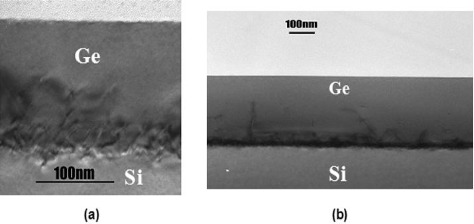
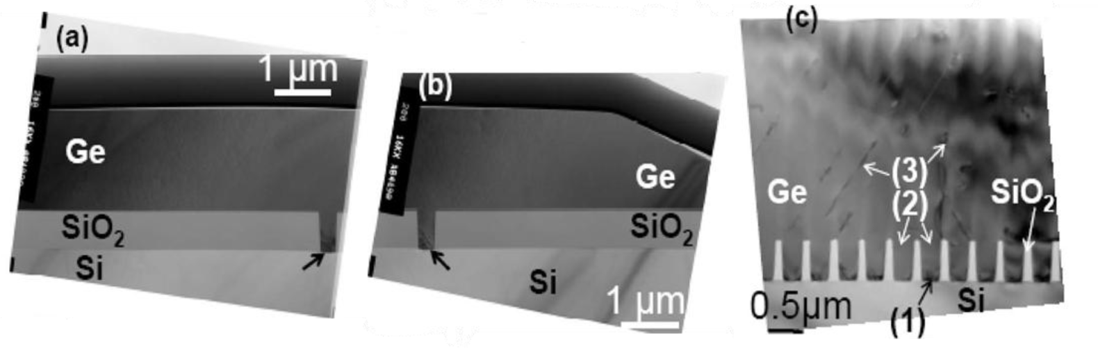
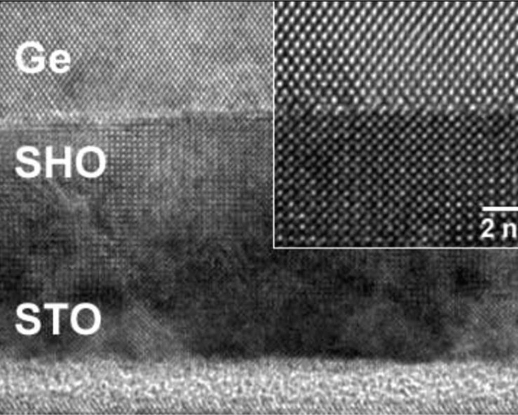
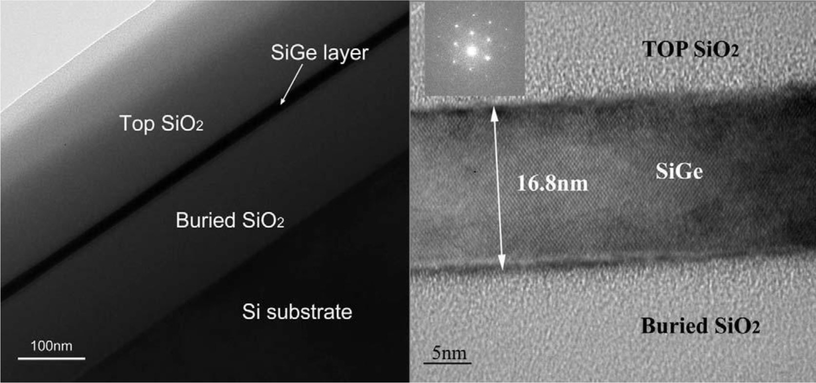
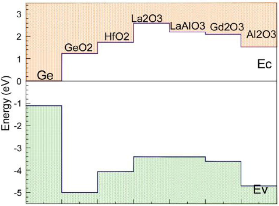
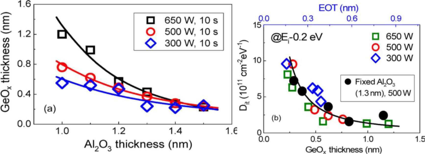
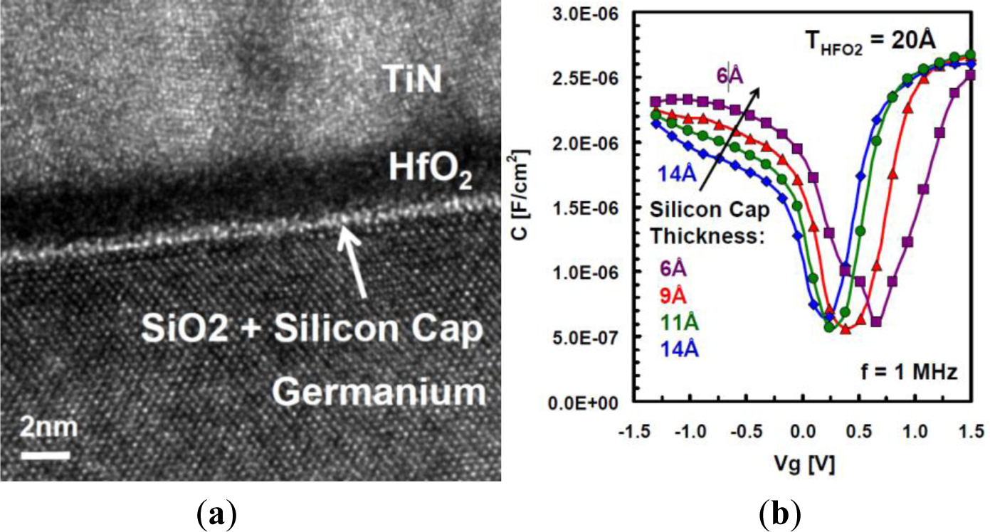
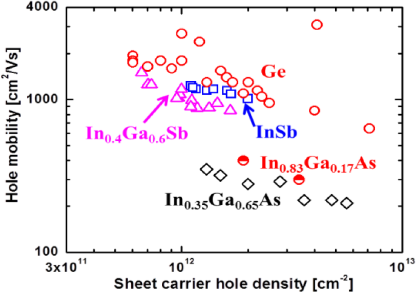
| Category | Approach | Details | Substrate | Bandgap of buffer material (eV) | Total thickness (nm) | Ref. |
|---|---|---|---|---|---|---|
| Direct Epitaxy | Multiple hydrogen annealing for heteroepitaxy (MHAH) | direct epitaxy of Ge; multiple cycles of growth (400 °C) and high temperature hydrogen annealing (700–800 °C) | standard bulk Si | 0.67 | 400 | [36,37] |
| Multiple cycles of low temp, high temp, hydrogen annealing | (i) deposit Ge directly on Si at low temp; (ii) deposit Ge at high temp onto low temp layer; (iii) high temperature hydrogen annealing; (iv) repeat (i) to (iii) 3 or 4 times | Si(100) 4° offcut towards <110> | 0.67 | 2400 (4 cycles) 1400 (3 cycles) | [38] | |
| Graded SiGe Buffer | Step graded Si1–xGex buffer | 0.8 um Si0.1Ge0.9, followed by 0.8 um Si0.05Ge0.95, followed by 1 um Ge (all at 400 °C); 750 °C annealing between layers. | Si (100) 6° offcut towards <110> | 0.67–1.12 | 3600 | [39] |
| Step graded Si1–xGex buffer | (i) 0.5–1.0 um Si0.7Ge0.3 layer grown on Si; (ii) 0.3 to 1.0 um Si0.3Ge0.7; (iii) 10–50 nm phos. doped Si0.3Ge0.7 to suppress parallel conduction; (iv) 0.5–3.0 um Si0.3Ge0.7. | Si | 0.67–1.12 | ~1550 (est. from TEM image) | [15] | |
| Continuously Graded Si1–xGex and chemical-mechanical polishing (CMP) | (i) Graded from Si to Si0.5Ge0.5 at 10% Ge um-1; (ii) 1.5 μm Si0.5Ge0.5 cap; (iii) top 5 μm removed by CMP; (iv) Si0.5Ge0.5 graded to Si0.08Ge0.92 at 10% Ge um−1; (v) 1.5 um Ge cap. | Si(100) 6° offcut towards <110> | 0.67–1.12 | 12000 | [40] | |
| Surfactant-Mediated Epitaxy | A surfactant (Sb) is used to alter the strain-relief mechanism in Ge on Si epitaxy | One monolayer (ML) of Sb is deposited on the Si substrate followed by 1 μm of Ge; a high Sb flux of ~2.4 ML/min is maintained during Ge growth. | Si(100) | 0.67 | ~1000 | [41] |
| Aspect Ratio Trapping | ART combined with epitaxial lateral overgrowth (ELO) and CMP | Ge is grown in patterned trenches in thermally grown SiO2; dislocations terminate on trench sidewalls; lateral Ge growth begins beyond trench height; CMP used to flatten the surface. | Si(100) | 0.67 | ~1000 | [42] |
| Oxide Buffer | Ge condensation technique | Epitaxial SiGe layers are grown on silicon-on-insulator (SOI) substrates followed by successive thermal oxidation. | strained and unstrained SOI | not reported | not reported | [43] |
| Epitaxial SHTO buffer | (i) Epitaxial SrTiO3 is deposited using method in ref. [44]; (ii) epitaxial SrHfxTix-1O3 grown; (iii) Ge grown in two steps, 610 °C for nucleation, then 350 °C for homogenous coverage. | Si(100) | 3.5 (STO) 6.5 (SHO) [45] | ~ 20 (est. from TEM image) | [46] | |
| GaAs Buffer | GaAs nucleation and buffer layer | An InGaAs QWFET heterogeneously integrated on Si was demonstrated using this buffer. | Si(100) 4° offcut towards <110> | 1.42 | 500 | [25] |
| k | Gap (eV) | |
|---|---|---|
| SiO2 | 3.9 | 9 |
| Si3N4 | 7 | 5.3 |
| Al2O3 | 9 | 8.8 |
| Ta2O5 | 22 | 4.4 |
| TiO2 | 80 | 3.5 |
| SrTiO3 | 2000 | 3.2 |
| ZrO2 | 25 | 5.8 |
| HfO2 | 25 | 5.8 |
| HfSiO4 | 11 | 6.5 |
| La2O3 | 30 | 6 |
| Y2O3 | 15 | 6 |
| α-LaAlO3 | 30 | 5.6 |
© 2014 by the authors; licensee MDPI, Basel, Switzerland This article is an open access article distributed under the terms and conditions of the Creative Commons Attribution license (http://creativecommons.org/licenses/by/3.0/).
Share and Cite
Goley, P.S.; Hudait, M.K. Germanium Based Field-Effect Transistors: Challenges and Opportunities. Materials 2014, 7, 2301-2339. https://doi.org/10.3390/ma7032301
Goley PS, Hudait MK. Germanium Based Field-Effect Transistors: Challenges and Opportunities. Materials. 2014; 7(3):2301-2339. https://doi.org/10.3390/ma7032301
Chicago/Turabian StyleGoley, Patrick S., and Mantu K. Hudait. 2014. "Germanium Based Field-Effect Transistors: Challenges and Opportunities" Materials 7, no. 3: 2301-2339. https://doi.org/10.3390/ma7032301