
Design and Implementation of Improved Gate Driver Circuit for Sensorless Permanent Magnet Synchronous Motor Control


1
Department of Life Science and Systems Engineering, Graduate School of Life Science and Systems Engineering, Kyushu Institute of Technology, Kitakyushu 808-0196, Fukuoka, Japan
2
Department of Electrical Engineering, Politeknik Elektronika Negeri Surabaya, Surabaya 60111, East Java, Indonesia
*
Author to whom correspondence should be addressed.
World Electr. Veh. J. 2024, 15(3), 106; https://doi.org/10.3390/wevj15030106
Submission received: 6 December 2023
/
Revised: 5 March 2024
/
Accepted: 6 March 2024
/
Published: 9 March 2024
(This article belongs to the Special Issue Permanent Magnet Motors and Driving Control for Electric Vehicles)
Abstract
:Reliable motor control is important for electric vehicle applications. The control process requires accurate measurements of the current and rotor position information to establish correct motor control design, particularly in sensorless permanent magnet synchronous motor control systems. Practical issues regarding the motor control circuit, such as the effects of parasitic element behavior on the switching components in the insulated gate bipolar transistor-driven inverter, were discussed in this study. It analyzed the effects of parasitic elements that can cause the ringing of switching losses and affect the spike of the signal in the motor current, which must be avoided in the implementation of motor control. The gate driver circuit topology was improved to reduce this effect in motor control devices. The proposed gate driver circuit design with the ringing suppression circuit configuration achieved good performance by keeping the signal spike at less than 10% in the motor current. Furthermore, a signal spike or noise was not observed in the estimation results of rotor position when using current information as the parameter control process. Both conditions were verified by experiments on the designed motor control devices. Under these conditions, signal precision can be achieved in motor control.
1. Introduction
Awareness of environmental issues, including the depletion of natural resources, increasing levels of pollution, significant greenhouse gas emissions, and rising global temperatures, is an important factor promoting the use of electric vehicles (EVs) as a viable solution [1,2,3]. The motor controller is a fundamental control component of EVs, has significant effects on the efficiency of the drive system, and is related to the comfort design of EVs [4,5,6]. Hence, it is meaningful to investigate the motor controller in EV applications.
Permanent magnet synchronous motors (PMSM) are the most promising solution for power drive systems, including EVs, and are characterized by a robust structure, high power density, high efficiency, and a wide speed range [7,8]. The implementation of advanced sensorless motor control is rapidly being developed to improve motor drive performance in EVs. Sensorless motor control systems offer sophisticated computational control algorithms for reducing the cost of sensors, simplifying the wiring system, and reducing the overall size of the system [8,9,10]. To obtain superior motor drive control, in addition to advanced computational algorithms in the motor control process, the control circuit also plays an important role in EV applications [9,10,11,12]. The accuracy of the motor control process is influenced by the motor control circuit. The precision of the signal must be maintained to achieve good performance in the control process. An important problem is the behavior of the power switching components [13,14,15]. In this case, the effect of power switching components influences the signal information used in motor control processing, such as current information and the motor rotor position. Many studies have reduced this effect by implementing compensation using digital processing in computing systems [15,16]. However, because this does not significantly weaken the effect of the switching component behavior, this effect still occurs in the motor drive control system. This study focused on improving the motor control circuit by considering the effect of the switching component behavior in an insulated gate bipolar transistor-driven inverter (IGBT-Driven Inverter). Based on the analysis of the behavior of switching components, which causes ringing flow, a ringing suppression circuit is used to overcome this effect. An integrated system consisting of a hardware motor control process and a motor control circuit is implemented into the design of motor control devices that can be used for the development of EVs with motor control capabilities.
To achieve loss reduction in the control circuit and a high precision of the control process in actual motor control applications, extensive research has been conducted to improve the motor drive control process. In [17], a bootstrap circuit was proposed to reduce the switching loss in gate driver design. The implemented system incorporated a mitigation circuit for performance improvement. The acceleration of the switching process and the reduction in switching losses can be obtained through the simple circuit proposed by the above-mentioned study. However, practical issues regarding component behavior in the integrated system were not discussed, although this condition should be considered to enhance the gate driver performance. In [18], the switched inductor (SL) technique was applied to reduce the current stress in the converter design and mitigate the resulting current ripple. Current stress analysis was carried out on the DC–DC converter system to optimize the SL performance by reducing the current ripple. The findings revealed that reducing the current ripple in the system can reduce the power loss and switching loss. Therefore, current precision is an important consideration for improving the performance of the power converter system. A previous study [19] focused on the failure operation in a high–low side inverter driver. A bootstrap circuit can protect the switching operation when the supply voltage drops. This circuit is suitable for the half bridge inverter configuration used in motor control applications. In actual motor control implementations, many electronics systems must operate with several parts to facilitate the control process. Therefore, the gate driver circuit should perform well to ensure a smooth and safe process. In [20], the Optoisolator integrated circuit (IC) provided good protection when implemented in motor control. Based on the controlled concept in transistor–transistor logic, gate driver circuit design can be achieved. For efficient design, the component usage should be minimized. Consequently, the number of protection components in each side (two components) should be minimized. Additionally, motor control systems proceed using a chopper drive and simple-structure devices, but the probability of failure or the noise spike effect have not been investigated. In [21], compensator design was implemented for an IGBT-driven inverter. The discrete system employed by a field programmable gate array (FPGA) introduces additional execution time requirements for computational systems. A previous study [22] investigated the compensator for the voltage source inverter in the EV motor controller and proposed a design motor control circuit. The losses from IGBT switching that impact overshoot and transient behavior under ideal conditions were investigated via simulation. In this case, practical issues in the motor controller process can be observed clearly only through simulation. Therefore, it is important to investigate the precision parameter used in the input control process. In [23], actual PMSM motor control was implemented in the FPGA system, and the structure and computation of the control process were explained, focusing on the precision of the motor current as the input of the motor control process to improve the control procedure. The compensator in analog to digital converter (ADC) system design in the FPGA block function aims to reduce the signal spike in the motor current. Notably, the actual motor current includes substantial noise. In [24], the hardware design of the motor control circuit was presented. The printed circuit board (PCB) layout of the implemented hardware system must be considered in the current measurement process. Because many motor control implementations employ vector control in the motor control process, PCB design for motor control hardware emphasizes the optimization of the current measurement results. To improve the performance of the motor control system in the proposed hardware design, system losses should be minimized, the measurement method should be improved, and the precision of vector control in the motor control process should be better maintained. A previous study [25] realized a sensorless PMSM based on the Back-EMF observer using machine learning, which was used to adjust certain motor measurement parameters. By reducing noise in the machine learning approach, results were obtained with high accuracy. Another study [26] investigated the application of modern control techniques by considering several conditions to test the control response. The above-mentioned study showed the influence of signal noise effects on the optimization of the control response, such as the time required to reach steady-state conditions. Therefore, in modern control implementations, high performance can be achieved by eliminating signal noise.
In summary, losses and spikes should be avoided to obtain precise results for the motor control process. Some practical issues in the hardware control process when the motor control circuit was integrated should also be considered to achieve good motor control design. Moreover, for the high-precision control of sensorless PMSMs, the performance of the general motor control circuit and motor control process must be improved in actual motor control applications. The contributions of this study are as follows:
- The improved Gate Driver Circuit (GDC) of the IGBT-driven inverter reduces the power supply usage and provides a good isolation side in motor control applications.
- The motor control circuit design considers the parasitic element effect of the IGBT-driven inverter in motor control applications.
- The noise of the signal spike in the motor current was reduced to increase the effectiveness of the sensorless motor control application.
The rest of this paper is organized as follows. Section 2 explains the parasitic element analysis of the motor control circuit. The sensorless PMSM control technique based on Back-EMF estimation is presented in Section 3. In Section 4, the details of the proposed improved GDC in the architecture of motor control devices are discussed. The experimental results and their verification are presented in Section 5. Finally, the conclusions are presented in Section 6.
2. Parasitic Element Analysis of IGBT-Driven Inverter for Motor Control
In the IGBT-driven inverter for the motor control device system, GDC design is essential. The interface performance of GDC is a vital consideration, owing to its ability to isolate the control side from the power inverter devices, and perform other optimization operations such as minimizing the switching losses affecting the signal spike in the motor current caused by the ringing switching behavior in the power inverter component. The equivalent circuit in Figure 1 describes the flow analysis of the ringing condition caused by the effect of parasitic elements in the power switching component. Here, are the capacitance and inductance, and represent the parasitic element of the gate, drain, and source in the power switching component, respectively; are the resistance, inductance, and induced voltage of PMSM as a load system, respectively.
In this system, the parasitic inductance in the ringing flow, denoted as , appears as a parasitic element on the source side when the DC source and are connected. Additionally, appears as AC and DC resistance in the ringing flow area. Parasitic inductance was connected in series with the drain and source in the power switching component, which affected the transition speed and peak voltage connected to the load. The voltage across the parasitic inductor during the ON-to-OFF transition or vice versa is expressed by Equation (2). During the ON transition, the drain output current increases and produces a positive voltage, owing to the effect induced by crossing the parasitic inductance, which causes a decrease in the effective voltage on the power switching device by inducing the occurrence of a voltage spike on the negative side. Moreover, during the OFF transition, the output current decreases and produces negative voltage, owing to the effect of crossing the parasitic inductance, which induces a voltage spike on the positive side. Based on these conditions, an additional circuit can be added to reduce the effect of parasitic inductance (), which increases significantly in high-frequency system implementations. The effect of parasitic inductance was represented in a ringing condition flow equivalent circuit for circuit analysis (Figure 2). Under the condition of voltage at and a constant source, the drain-to-source voltage can reach its peak as the drain output current value ID approaches zero. Additionally, if the input voltage at capacitor is less than the source voltage, owing to parasitic effects, and the output capacitor voltage is greater, the ringing flow condition can occur, as indicated by the blue dashed line (Figure 2a). The additional circuit uses a capacitor as the filter and a series-parallel capacitor-resistor as the ringing suppression circuit (Figure 2b,c) to provide a path by bypassing the resonance phenomena caused by parasitic elements. Thus, the circuit minimizes the effects of parasitic elements at high frequencies and prevents high-frequency currents from returning to the source. Thus, attenuation can be achieved under ringing flow conditions.
In practice, the capacitance value for the filter can be determined based on the minimum bootstrap capacitor value shown in the IC’s GDC datasheet. Furthermore, the capacitance and resistance values of the ringing suppression circuit are expressed by the following equations.
The voltage spike during the transition condition including the parasitic effect can be described as follows:
Owing to inductance, a parasitic effect occurs and causes a resonant condition, which can be expressed as follows:
The assumed voltage spike and resonant condition impact of the parasitic inductance effect can be analyzed by adding the capacitor and damping resistor. Therefore, the inductance parasitic elements of the circuit can be calculated as follows:
Additionally, ringing flow occurs when the switch is closed and a voltage source is connected to the series LC configuration of the parasitic element. Furthermore, to consider the damping ratio and frequency used for the circuit, the capacitance and resistance value of the ringing switching circuit can be described as follows:
where are the peak spike voltage in the ringing switching behavior, the voltage in the inductance parasitic, the drain current, and the floating current under the OFF condition, respectively; are the resonant frequency associated with the spike in the ringing flow, the frequency value of ringing flow provided by the original capacitance effect in the semiconductor component, the resonant value of ringing flow by the original capacitance effect in the semiconductor component with an additional external capacitance, and the switching frequency, respectively; and , and ξ are the inductance in parasitic behavior, the capacitance of the ringing suppression circuit, the original capacitance value in the semiconductor component, the external capacitance indicating the parasitic effect in the ringing flow, the resistance of the ringing suppression circuit, the resistance of the pulldown and OFF condition, and the damping in the optimal design of the ringing suppression circuit, respectively. Based on the above explanation, the GDC design should consider the effect of the parasitic element to improve the performance by minimizing the switching losses caused by the ringing switching behavior of the semiconductor components, which is important for achieving reliable motor control.
3. Back-EMF Observer Technique for Sensorless PMSM
In this study, the sensorless PMSM motor control was operated in a wide range of speeds (medium to high). The Back-EMF estimated using the observer technique can be used to obtain the rotor position information in the speed range. In this study, the full-order state observer was used to estimate the Back-EMF. The observer model for Back-EMF estimation was designed using motor parameters (motor resistance () and motor inductance ()) and motor variable measurements (voltage or current). In this case, estimation can be performed because Back-EMF has a correlation in three phase reference frames with the speed and rotor position information of the PMSM motor, as shown in Figure 3. Specifically, the Back-EMF estimation model for the PMSM motors can be formulated as follows [11]:
where are the stator voltage in each phase, the stator current in each phase, the resistance of the armature, and the self-inductances of the motor, respectively; p, are the differential operator , the Back-EMF constant in , and the rotor speed, respectively.
The PMSM motor used in this study was a surface-mounted permanent magnet synchronous motor (SPMSM). The correlation of Back-EMF in the SPMSM motor equation in the stationary frame can be described as follows:
where ,, ,, , are the stator voltage, stator current, and induced voltage (Back-EMF) in the αβ reference frame, respectively.
According to Equation (9), the Back-EMF estimation in the full-order observer was implemented using alpha-beta current information (, and the gain vector can be represented by a matrix when the Back-EMF axes are assumed as follows:
Based on the observer result, the estimated rotor position and rotor speed can be expressed as follows:
where , , , and are the estimated position of the rotor, the speed estimation of the rotor, the Back-EMF in the alpha (α) axis, and the Back-EMF in the beta (β) axis, respectively. In this case, the design of the observer model is highly dependent on the current signal to obtain the Back-EMF estimation result. Therefore, the accuracy of the motor control process and rotor position estimation can be maintained by minimizing the interference or noise in the signal.
4. Improvement GDC of IGBT-Driven Inverter for Motor Control Circuit
This section provides a detailed explanation of the improvement of the motor control circuit. Figure 4 shows the architecture of the integration of the circuit design and control process into the motor control device. The proposed improvement was implemented in the architecture of the motor control device to observe the performance in the sensorless PMSM control application.
In this study, the improved GDC using Infineon IC of the IR2110 with a ringing suppression circuit focused on IGBT-driven inverter design. In this case, the arrangement location of the component that caused the increasing temperature parasitic effect is not considered. Therefore, the system aims to provide a good isolation side and minimize switching losses. Additionally, the spike of the current signal that is suitable for implementation in sensorless motor control systems ignores the effect of temperature in the circuit. The basic function of GDC in the IGBT-driven inverter was explained earlier. The PWM signal generated by the FPGA has a voltage level of 3.3 V with limited current capability; therefore, it cannot be used directly to drive the IGBT-driven inverter, and the conditioning of the PWM signal level via amplification and the provision of an adequately isolated side are required. In this case, the FOD 3182 optocoupler IC was used to amplify the signal and provide isolation functions in the GDC design. This IC could increase the PWM signal level to 15 V with a current capability of up to 1 A, and also provided good isolation conditions (Figure 5).
Subsequently, the amplified and isolated PWM signal was applied to the IR2110 gate driver IC to generate high- and low-side signals, which were used to drive the IGBT on the inverter component. Contrary to previous studies and the typical configuration, the GDC using the IR2110 typically requires two power supplies, because the voltage levels on the input and output sides are different. However, in this study, the input and output voltage levels were the same, owing to voltage amplification, and one power supply was sufficient (Figure 6). Furthermore, by selecting an appropriate value, the maximum current can be drawn from the GDC to quickly charge the capacitance gate of the power inverter component when it is ON. The fast recovery diode FR207 and are used during the OFF state to ensure system safety against floating gate conditions when the power inverter component is not activated ( discharge including ).
Importantly, the effects of the parasitic elements that appear in the circuit, as explained in Section 2, should be minimized, because they can lead to switching losses and a current spike signal, which affect the control process (Figure 7). Generally, capacitor filters are used to overcome the resonance effects caused by parasitic elements. However, in systems that require precision and sensitivity, the circuit’s performance must be improved. A ringing suppressor circuit using a resistor and a capacitor installed in parallel series on the output pin (output to load) of the IR2110 is proposed as an improved IGBT-driven inverter. Because the pin is connected directly to the load, the parasitic element effect will influence the current flowing to the motor. Therefore, it is necessary to minimize this effect to reduce the current spike signal, which is used as important information in the motor control system. The detailed observations and correlation of the motor currents in motor control system applications are discussed in more depth in Section 5.
Additionally, the effect of parasitic elements in the circuit affects the switching gate signal connected to the inverter component. Therefore, to evaluate the performance of circuit improvements, the reduction in the effect of parasitic elements can be easily identified by observing the PWM signal generated to control the inverter. The impact of the parasitic element on the system decreases proportionally with the occurring spike. This study compared three GDC configurations, namely the GDC design using the IR2110PBF IC gate driver as a typical configuration, a configuration with the addition of a filter circuit, and an improved configuration with the addition of a ringing suppression circuit. The three schematic diagrams of each configuration are shown in Figure 7.
Test results for the ringing switching conditions of power switching components obtained referred previous studies [27] were used to observe the presence of parasitic phenomena under these conditions (Figure 8a). Based on the observation results (Figure 8b,c), the use of capacitors as a filter circuit installed in parallel on the high and low sides minimized the spike conditions by up to 75% in the PWM signal of the power inverter compared with using them in the typical configuration. However, the effectiveness of minimizing these conditions must be improved to achieve superior performance.
The result of the improved configuration using a ringing suppression circuit appears to have superior performance in minimizing the spike condition at the GDC output (Figure 8d). In this study, the voltage spike did not exceed 1.75% of the nominal PWM voltage, because the resistance function (Equation (7)) was applied as a damping system when the ringing condition was caused by the parasitic effect of the element. Therefore, in the improved GDC configuration, the ringing suppression circuit implemented using the series-parallel circuit of the capacitor and resistors connected to the load is suitable.
Figure 9 shows the results of the prototype laboratory motor control device. A sensorless PMSM was used as a controlled object by installing two current sensors to obtain the motor current information. The dependency on the current information and rotor position is critical in the processing of the control system. The improvements in the motor control circuit design achieved in this study are expected to mitigate factors affecting the control process computation. Thus, the effective use of motor control devices can be achieved to realize motor control applications.
5. Experimental Results
To evaluate the practical performance of the proposed laboratory prototype motor control device design, the experimental setup is shown in Figure 10. Tests were conducted on the implementation of the PMSM sensorless motor control using the Back-EMF estimation obtained by the observer method. In this study, the motor was operated in the speed range of 1000–3000 rpm, and the Back-EMF estimation was satisfactory. The Back-EMF estimation results were only used to show the dependence on the precision of the motor current information as an observer input parameter. The experimental results revealed the current signal spikes caused by the effects of parasitic elements in the motor control circuit affect the estimation result. The very strong dependence on the precision of motor current information, as expressed by Equations (12) and (13) in Section 3, shows that the reduction in current signal spikes is expected to improve the motor control performance and estimation of rotor position. Several tests were carried out to evaluate the performance of each circuit configuration in reducing the current signal spikes. Two current sensors were installed in phase A and phase B as variable information to design the observer model for the Back-EMF estimation and motor control process. In this case, the results of the current sensor readings for each phase were processed by the analog to digital converter and digital to analog converter system and were displayed on the Memory Hi-CORDER to simplify the evaluation and analysis process. The detailed specifications of the supporting equipment used in the experimental setup are presented in Table 1.
The experimental comparison results are presented in Table 2. Several tests were performed on the proposed motor controller device with a switching frequency of 25 kHz. The first test was conducted on the integration of the sensorless PMSM motor control system with the motor controller device using a typical GDC IR2110 configuration (Figure 7a). In this study, the system performance evaluation regarding the parasitic element effect for switching losses during the transition condition from OFF to ON was observed as described in Section 4. Furthermore, the parasitic element effect induced by the spike of the signal in the motor current on the motor control device was observed. Figure 11 shows that the inverter output current waveform connected to the motor experienced an average current spike of more than 33%, which is more than 1A under the peak current conditions of 3A. In this case, this condition occurred for 4 ms in one cycle. The results reveal that the parasitic element effect on the power inverter component caused the ringing switching loop phenomenon, which affected the inverter current.
The analysis of the parasitic element revealed that the correlation between the ringing condition and the current spike, which causes signal noise and occurs in the inverter, can be easily identified by the equivalent of a resonant circuit. As is known, the current waves in phase A and phase B have large current signal noise (Figure 11a,b). These conditions should be avoided to ensure that the control process is working well. Moreover, the computation of the control process and Back-EMF observer technique implies dependence on the motor current information. Figure 11c shows that there is a noise signal in the rotor position estimation owing to the spike of the current signal in the motor. Therefore, precise motor current information is required to achieve satisfactory motor control performance.
The GDC configuration with the addition of a capacitance filter in each section of the high and low side gate drivers (Figure 7b) was implemented in the second motor device control test to minimize the spikes in the motor current. However, based on the results shown in Figure 12, the performance of the motor controllers was still suboptimal because the spike of the current signal in phase A and phase B was still quite large—that is, approximately 30% under the peak current conditions of 3A (Figure 12a,b). Although the spike oscillation time under this condition was shorter by 2 ms compared with that with the typical configuration, this condition still affected the spike of the current signal of the motor and reduced the accuracy of the rotor position estimation results (Figure 12c). Therefore, further effort is needed to minimize spike occurrence and improve the performance of motor controllers.
The third test was performed based on the improved GDC configuration using a ringing suppression circuit to minimize spike occurrence. In this study, this configuration (Figure 7c) was applied to control the proposed motor devices in the sensorless PMSM motor control system. As shown in Figure 13, the performance of the improved circuit is satisfactory. In this case, when the output current inverter is connected to the motor, the current spike can be properly minimized. Based on the test results (Figure 13a,b), the current waveform is consistently smoother. In the event of a current spike, the maximum did not exceed 10% of the peak current of 3A, and the oscillation time was approximately less than 1 ms. These conditions contribute to satisfactory performance in terms of maintaining current motor information. Therefore, the computed control process is satisfactory. Moreover, minimizing the noise spike of the current signal in phase A and phase B can also maintain the rotor position estimation, which is a better result, as shown in Figure 13c.
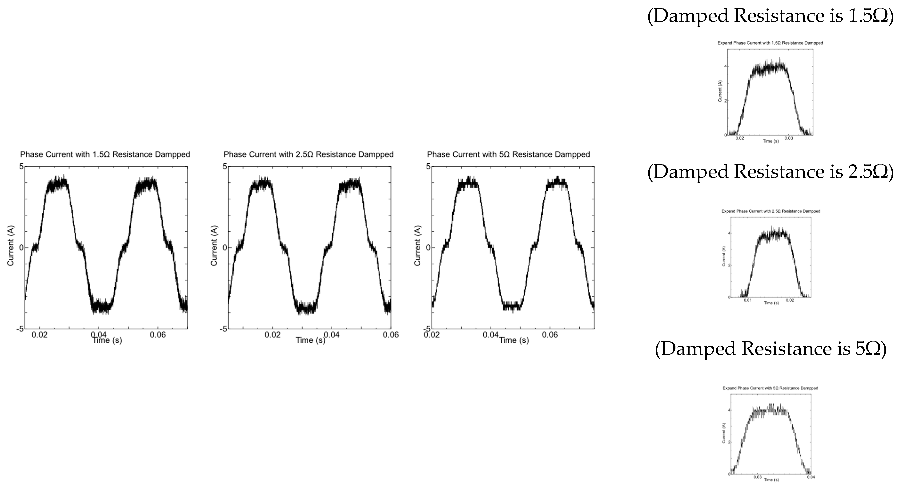
To achieve optimal performance for the proposed improved circuit, it is imperative to test it with various values of the components used. In this case, the resistance in the ringing suppression circuit acts as a damper to minimize the effect of parasitic elements. Therefore, according to Equation (7), the change in element damping causes the change in the resistance value. A higher setting for the damping element implies a greater resistance value. As shown Figure 14, with a higher resistance value in the ringing suppression circuit, the spike of the current signal becomes smaller, which is desirable in the control process implementation, because a low noise signal is provided.
Table 2 summarizes the performance results for each configuration circuit. Given the dependency on motor current information, circuit improvement is important for achieving a precise signal.
Based on the experimental results, the improved circuit of GDC in the motor control circuit, particularly the part of the IGBT-driven inverter, is significantly better than the typical configuration and additional capacitance filter. In this study, the reduction in the current spike, which affects the noise of the current signal, can be achieved to provide precise current information for use in the control process computation. Therefore, to achieve good performance, the motor current should have a small noise signal. Additionally, owing to the technique used for estimating the rotor position, the current motor information is also required. Hence, these conditions are expected to provide satisfactory estimation results. The experimental results reveal that the proposed motor control devices can be used as an alternative for improving the performance of industrial motor controllers.
6. Conclusions
This paper proposes the implementation of motor control devices for sensorless PMSM based on the Back-EMF observer technique. The parasitic element effect in the motor control circuit, motor control circuit design, speed and position estimation technique, and details of the improved circuit in the architecture of motor control devices were discussed. The improvement of motor control circuit design, particularly that of GDC, was explained, which can be helpful in obtaining accurate information for the motor control process parameters. For the PMSM motor control, a certain block transformation control process is required for execution in computational systems that use motor current information. Therefore, spikes in signal noise should be avoided to achieve good performance. Additionally, if the applied rotor position and motor speed estimation technique has a strong dependence on the motor current information, minimizing spikes in signal noise can provide better estimation results. The experimental results reveal that the designed motor control circuit performs well in minimizing spikes in signal noise in the motor current. When the motor control devices were used in the motor control process, the spike in the signal in the motor current was reduced by 20%, and the spike of the signal time was reduced to less than 1 ms. Therefore, the motor control process performance is satisfactory. In future work, the realization of sensorless PMSM control with high accuracy and high performance can be achieved in motor control devices for motor control applications in EVs.
Author Contributions
The manuscript preparation including system design and experiments was carried out by I.F. under the supervision of T.H. The analysis of data by I.F and T.H. has also contributed to manuscript correction. All authors have read and agreed to the published version of the manuscript.
Funding
This research received no external funding.
Data Availability Statement
The original contributions presented in the study are included in the article, further inquiries can be directed to the corresponding author.
Conflicts of Interest
The authors declare no conflict of interest.
References
- Men, X.; Guo, Y.; Wu, G.; Chen, S.; Shi, C.; Li, A.; Yuan, W.; Li, S.; Wang, X.; Qiu, X.; et al. Implementation of an Improved Mo-tor Control for Electric Vehicles. Energies 2022, 15, 4833. [Google Scholar] [CrossRef]
- Aiso, K.; Akatsu, K. Performance Comparison of High-Speed Motors for Electric Vehicle. World Electr. Veh. J. 2022, 13, 57. [Google Scholar] [CrossRef]
- Dhanamjayulu, C.; Padmanaban, S.; Ramachandaramurthy, V.K.; Holm-Nielsen, J.B.; Blaabjerg, F. Design and Implementation of Multilevel Inverters for Electric Vehicles. IEEE Access 2020, 9, 317–338. [Google Scholar] [CrossRef]
- Zaman, U.K.U.; Khan, U.S.; Bin Aqeel, A.; Zeb, A.; Ali, S.H.; Athar, U.; Jehangir, E.; Saif, M.M. Design and Development of Motor Controller and Electronic Differential System for Electric Vehicle Conversion. In Proceedings of the 2021 International Conference on Robotics and Automation in Industry (ICRAI), Rawalpindi, Pakistan, 26–27 October 2021; pp. 1–5. [Google Scholar] [CrossRef]
- Sieklucki, G.; Kara, D. Design and Modelling of Energy Conversion with the Two-Region Torque Control of a PMSM in an EV Powertrain. Energies 2022, 15, 4887. [Google Scholar] [CrossRef]
- Tomar, P.S.; Sandeep, N.; Verma, A.K.; Srivastava, M. Analysis, design, and implementation of an improved gate driver for high switching frequency EV application. IET Power Electron. 2020, 13, 1797–1806. [Google Scholar] [CrossRef]
- Yang, W.; Guo, H.; Sun, X.; Wang, Y.; Riaz, S.; Zaman, H. Wide-Speed-Range Sensorless Control of IPMSM. Electronics 2022, 11, 3747. [Google Scholar] [CrossRef]
- Wang, B.; Jiao, J.; Xue, Z. Implementation of Continuous Control Set Model Predictive Control Method for PMSM on FPGA. IEEE Access 2023, 11, 12414–12425. [Google Scholar] [CrossRef]
- Hattori, F.; Ushida, Y.; Sumiya, K.; Yanagisawa, Y.; Imaoka, J.; Noah, M.; Yamamoto, M. Frequency Doubler Gate Drive Cir-cuit Suitable for High-Frequency Applications. IEEE J. Emerg. Sel. Top. Power Electron. 2021, 10, 617–631. [Google Scholar] [CrossRef]
- Rook-Moon, K.; Lee, D. Analysis of Rotor Position Detection Performance According to the Frequency of Square Wave-form Voltage in the Harmonic Injection Sensorless Method through HILS. Processes 2021, 9, 2267. [Google Scholar] [CrossRef]
- Zhang, Z. Sensorless Back EMF Based Control of Synchronous PM and Reluctance Motor Drives—A Review. IEEE Trans. Power Electron. 2022, 37, 10290–10305. [Google Scholar] [CrossRef]
- Huang, Y.; Zhao, M.; Wang, Y.; Zhang, H.; Lu, M. An Improved Full-Speed Domain Sensorless Control Scheme for Permanent Magnet Synchronous Motor Based on Hybrid Position Observer and Disturbance Rejection Optimization. Electronics 2023, 12, 3759. [Google Scholar] [CrossRef]
- Anuragh, N.; Nath, S. Effect of Optocoupler Gate Drivers on SiC MOSFET. In Proceedings of the 2021 National Power Elec-tronics Conference (NPEC), Bhubaneswar, India, 15–17 December 2021; pp. 1–6. [Google Scholar]
- Yuan, B.; Xiao, L.; Wang, B.; Ying, J. High-Speed Dynamic Level Shifter for High-Side Bootstrapped Gate Driver in High-Voltage Buck Regulators. IEEE Trans. Circuits Syst. II Express Briefs 2021, 68, 3083–3087. [Google Scholar] [CrossRef]
- Xu, D.; Yang, M.; Hu, K.; Xu, D. A Transistor-Based Assist Gate Driver of SiC MOSFET for Crosstalk Suppression in a Phase-Leg Configuration. IEEE Access 2023, 11, 91247–91259. [Google Scholar] [CrossRef]
- Kumar, A.; Mandal, R.; Rushan, R.; Gauri, P. Design and Analysis of the Gate Driver Circuit for Power Semiconductor Switches. In Proceedings of the 2020 International Conference on Emerging Frontiers in Electrical and Electronic Technologies (ICEFEET), Patna, India, 10–11 July 2020; pp. 1–6. [Google Scholar]
- Qian, C.; Wang, Z.J.; Xin, G.; Shi, X. Partial-Bootstrap Gate Driver for Switching Loss Reduction and Crosstalk Mitigation. IEEE Trans. Power Electron. 2022, 37, 11523–11527. [Google Scholar] [CrossRef]
- Mollajafari, M.; Mohammadiazar, F.; Akbari, E.; Sheykhi, E.; Chaoui, H. A New Voltage-Multiplier-Based Power Converter Configuration Suitable for Renewable Energy Sources and Sustainability Applications. Sustainability 2022, 14, 16698. [Google Scholar] [CrossRef]
- Jin, W.; Cho, K. A Supply Voltage Noise Immunity Enhancement Design for High-Voltage Gate Driver IC based on Boot-strap Circuit. IEEE Trans. Circuits Syst. II Express Briefs 2021, 68, 3048–3052. [Google Scholar]
- Barman, P.; Baruah, P.; Sharma, S. An Optoisolator Based Gate Driver Design for Reliable Operation in High Power Motor Control Applications. In Proceedings of the 2021 International Conference on Advances in Electrical, Computing, Communication and Sustainable Technologies (ICAECT), Bhilai, India, 19–20 February 2021; pp. 1–6. [Google Scholar] [CrossRef]
- Wang, R.; Chen, Y.; Chen, J.; Liang, L.; Peng, L. Plug-in gate-loop compensators for series-connected IGBT drivers in a solid-state fault current limiter. CSEE J. Power Energy Syst. 2022, 8, 165–174. [Google Scholar]
- Sunardi, E.; Hindersah, H.; Rohman, A.; Zakaria, D. Compensator Design for Power Loss Reduction on IGBT Switching. In Proceedings of the 2023 International Conference on Computer Science, Information Technology and Engineering (IC-CoSITE), Jakarta, Indonesia, 16 February 2023; pp. 100–105. [Google Scholar]
- Milik, A.; Rudnicki, T. A Mixed Hardware-Software Implementation of a High-Performance PMSM Controller. Electronics 2023, 12, 440. [Google Scholar] [CrossRef]
- Triphati, P. Hardware Engineer’s Guide to a Brushless-DC Motor Controller: Design and challenges. IEEE Power Electron. Mag. 2022, 9, 40–45. [Google Scholar]
- Putra, D.S.; Chen, S.-C.; Khong, H.-H.; Chang, C.-F. Realization of Intelligent Observer for Sensorless PMSM Drive Control. Mathematics 2023, 11, 1254. [Google Scholar] [CrossRef]
- Negahban, M.; Ardalani, M.V.; Mollajafari, M.; Akbari, E.; Talebi, M.; Pouresmaeil, E. A Novel Control Strategy Based on an Adaptive Fuzzy Model Predictive Control for Frequency Regulation of a Microgrid with Uncertain and Time-Varying Parameters. IEEE Access 2022, 10, 57514–57524. [Google Scholar] [CrossRef]
- Zhang, Z.; Guo, B.; Wang, F. Evaluation of Switching Loss Contributed by Parasitic Ringing for Fast Switching Wide Band-Gap Devices. IEEE Trans. Power Electron. 2019, 34, 9082–9094. [Google Scholar] [CrossRef]
Figure 1.
Equivalent circuit and flow of ringing conditions in inverter including parasitic elements.
Figure 1.
Equivalent circuit and flow of ringing conditions in inverter including parasitic elements.

Figure 2.
Equivalent circuit and flow of ringing conditions in inverter including parasitic elements: (a) typical configuration; (b) configuration with capacitance in the high and low side; (c) configuration with a ringing suppression circuit of proposed systems.
Figure 2.
Equivalent circuit and flow of ringing conditions in inverter including parasitic elements: (a) typical configuration; (b) configuration with capacitance in the high and low side; (c) configuration with a ringing suppression circuit of proposed systems.
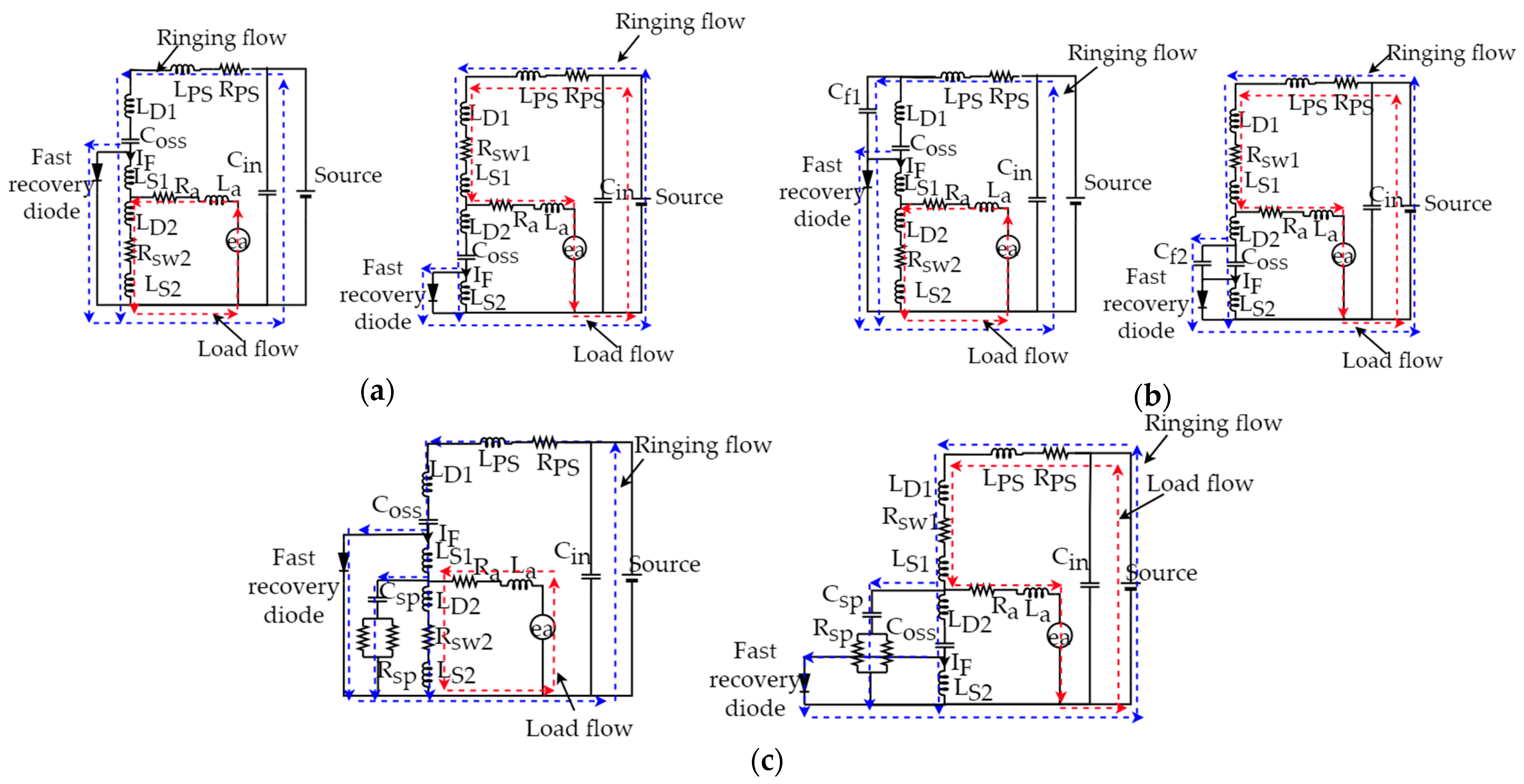
Figure 3.
Relationship between rotor position and speed of the motor in three reference frames.

Figure 4.
Architecture of the motor control device.
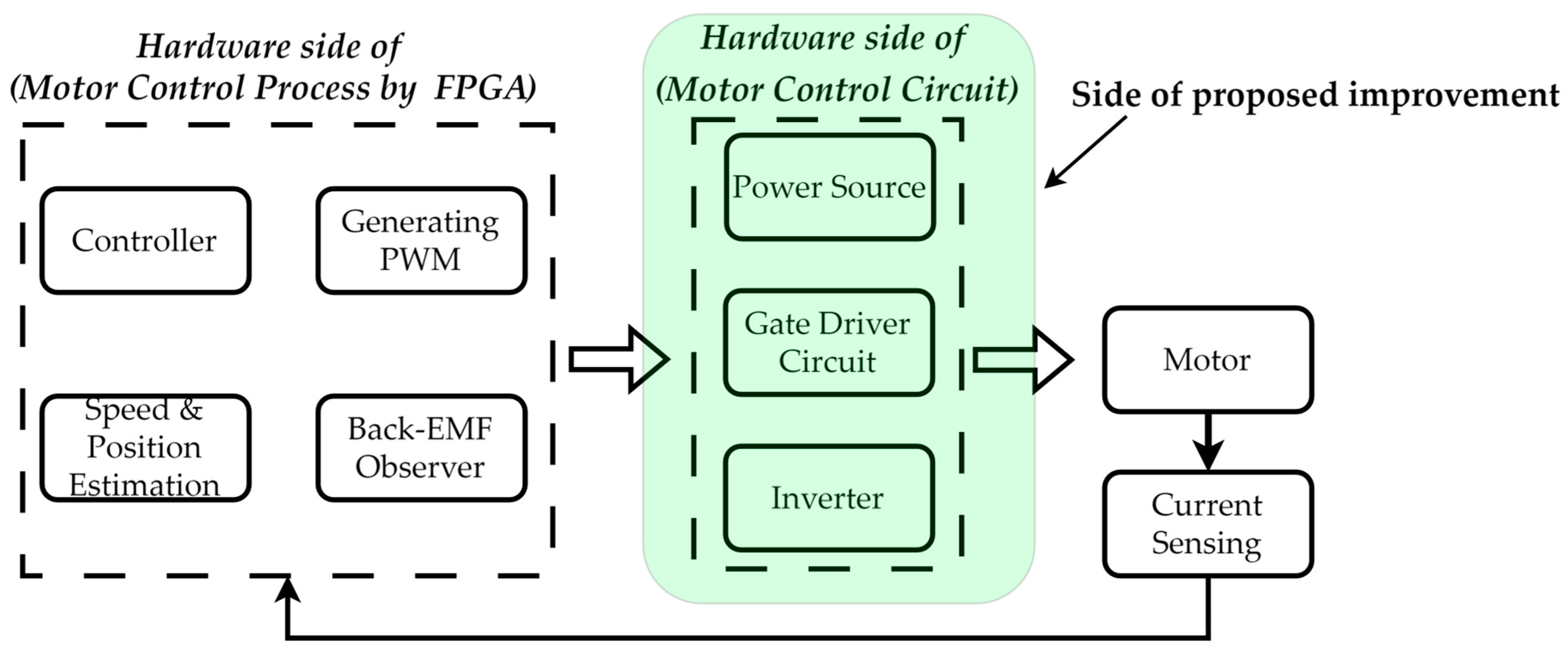
Figure 5.
Amplified and isolated PWM.
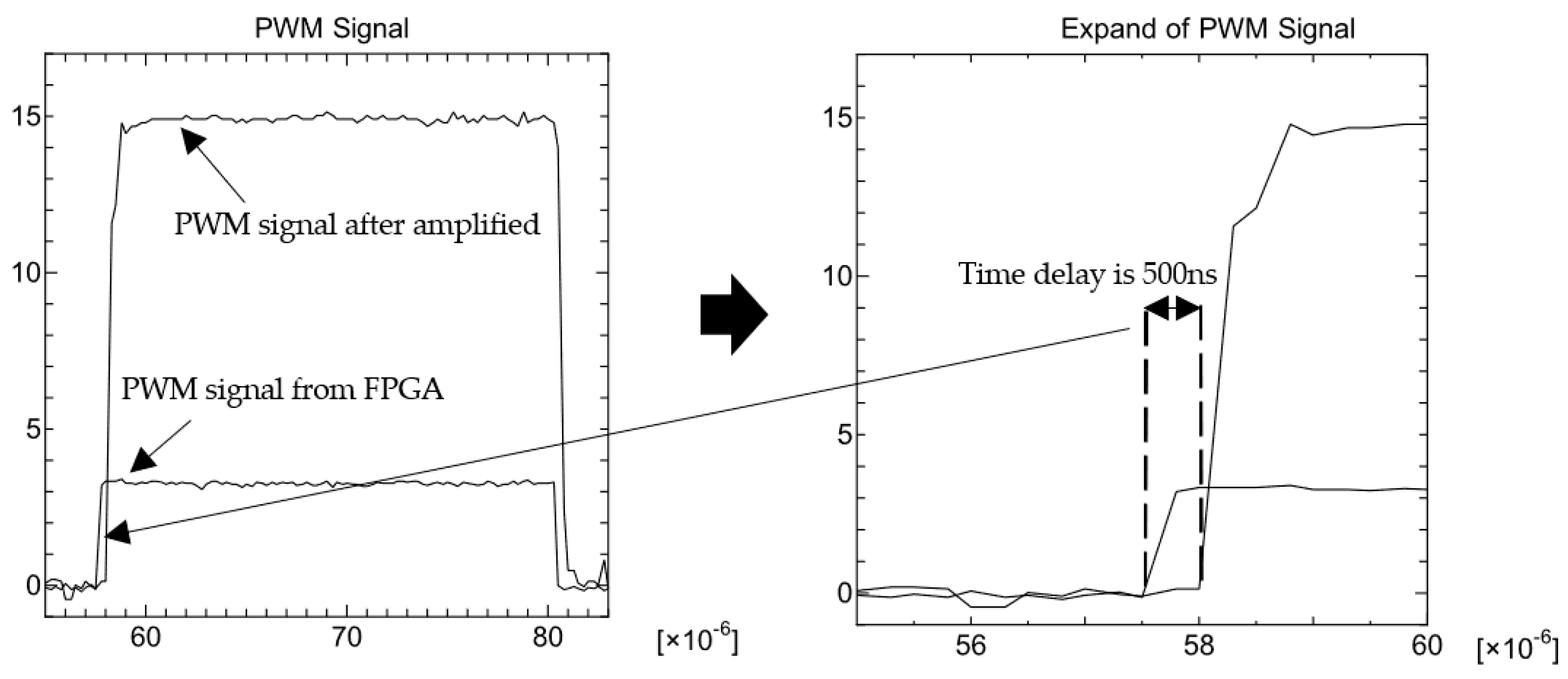
Figure 6.
Configuration of IC GDC using IR2110PBF: (a) typical configuration; (b) improved configuration with conditioning signal achieved through amplification and isolation side.
Figure 6.
Configuration of IC GDC using IR2110PBF: (a) typical configuration; (b) improved configuration with conditioning signal achieved through amplification and isolation side.
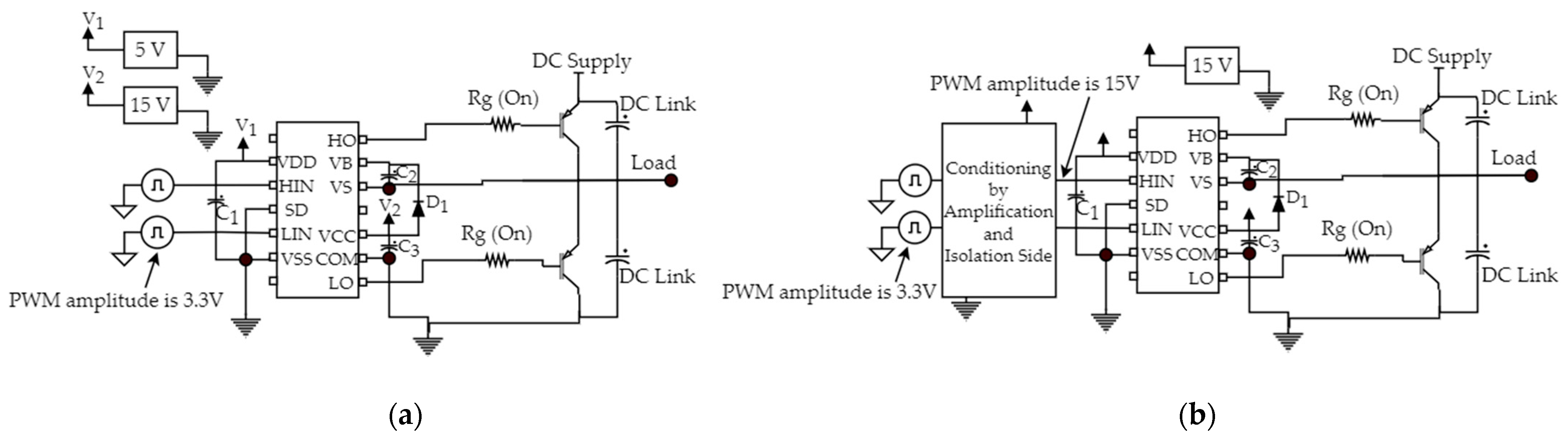
Figure 7.
Schematic of gate driver circuit using IR2110PBF with a conditioning and isolated side: (a) typical configuration; (b) configuration with capacitance in the high and low side; (c) configuration with a ringing suppression circuit of the proposed systems.
Figure 7.
Schematic of gate driver circuit using IR2110PBF with a conditioning and isolated side: (a) typical configuration; (b) configuration with capacitance in the high and low side; (c) configuration with a ringing suppression circuit of the proposed systems.
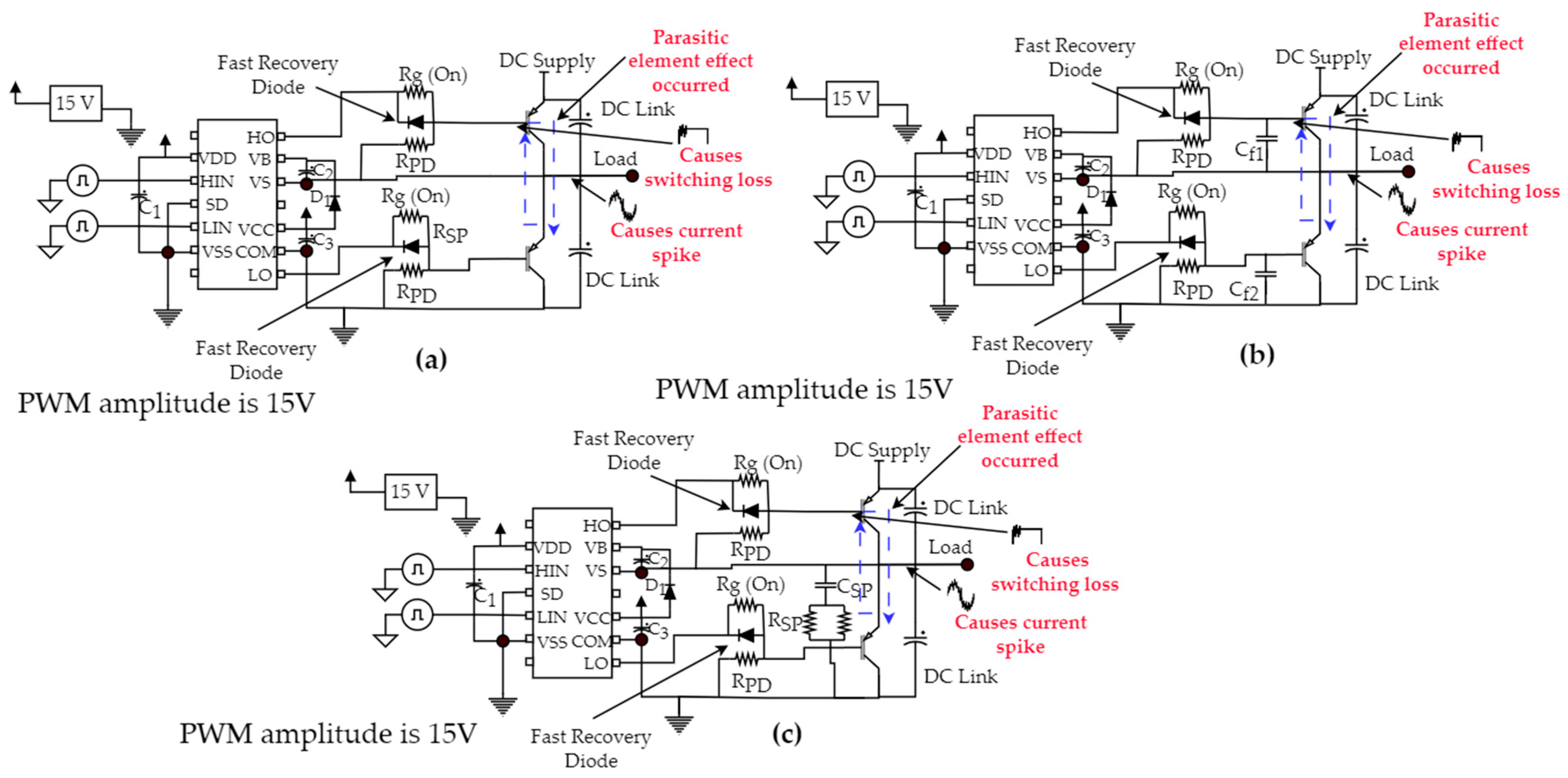
Figure 8.
Effect of ringing switching behavior in the semiconductor material: (a) the behavior of ringing in power switching component; (b) voltage spike in typical configuration; (c) voltage spike of configuration using capacitance in the high and low side; (d) voltage spike of configuration using a ringing suppression circuit of the proposed systems.
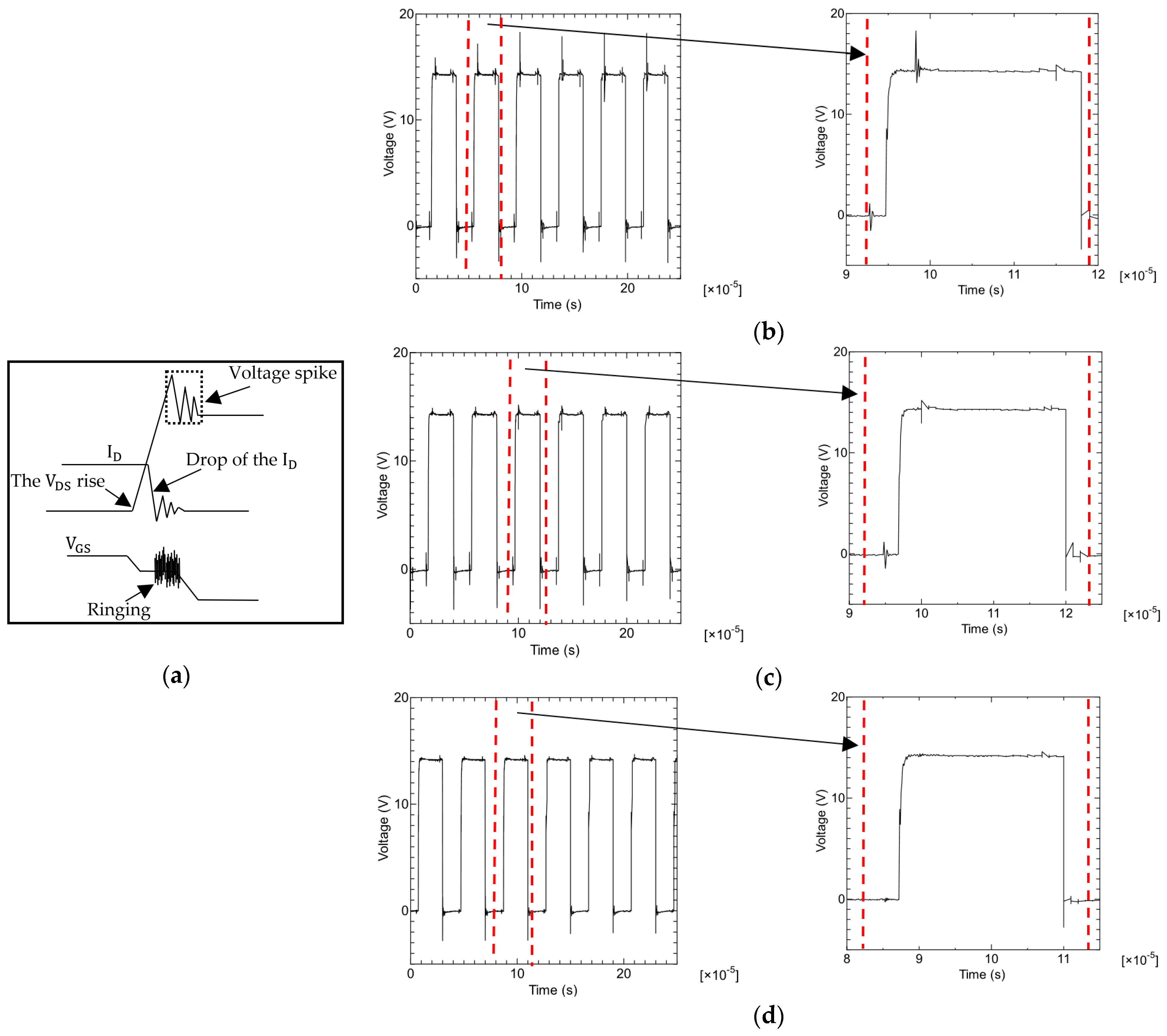
Figure 9.
Laboratory prototype of motor control devices.
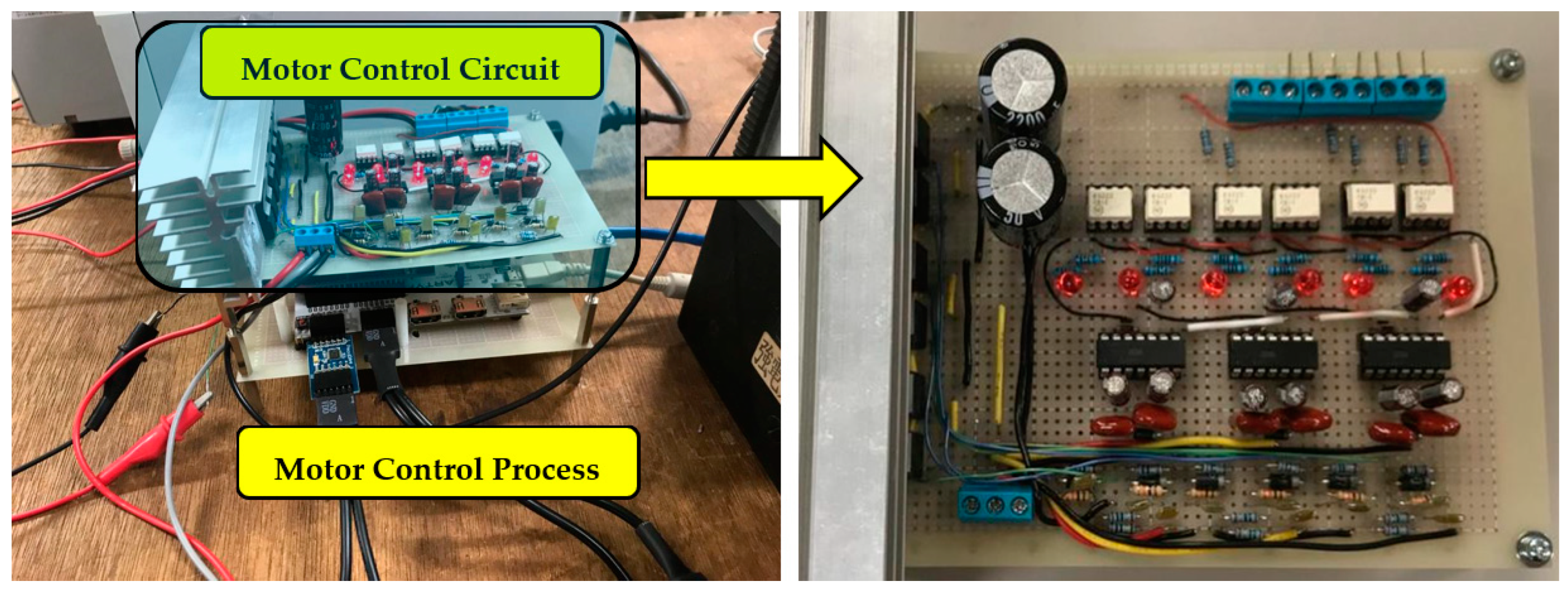
Figure 10.
Experimental setup.

Figure 11.
Observation results for motor control devices using GDC with a typical configuration IR2110: (a) current phase A in 3A; (b) current phase B in 3A; (c) rotor position estimation in 3A.
Figure 11.
Observation results for motor control devices using GDC with a typical configuration IR2110: (a) current phase A in 3A; (b) current phase B in 3A; (c) rotor position estimation in 3A.
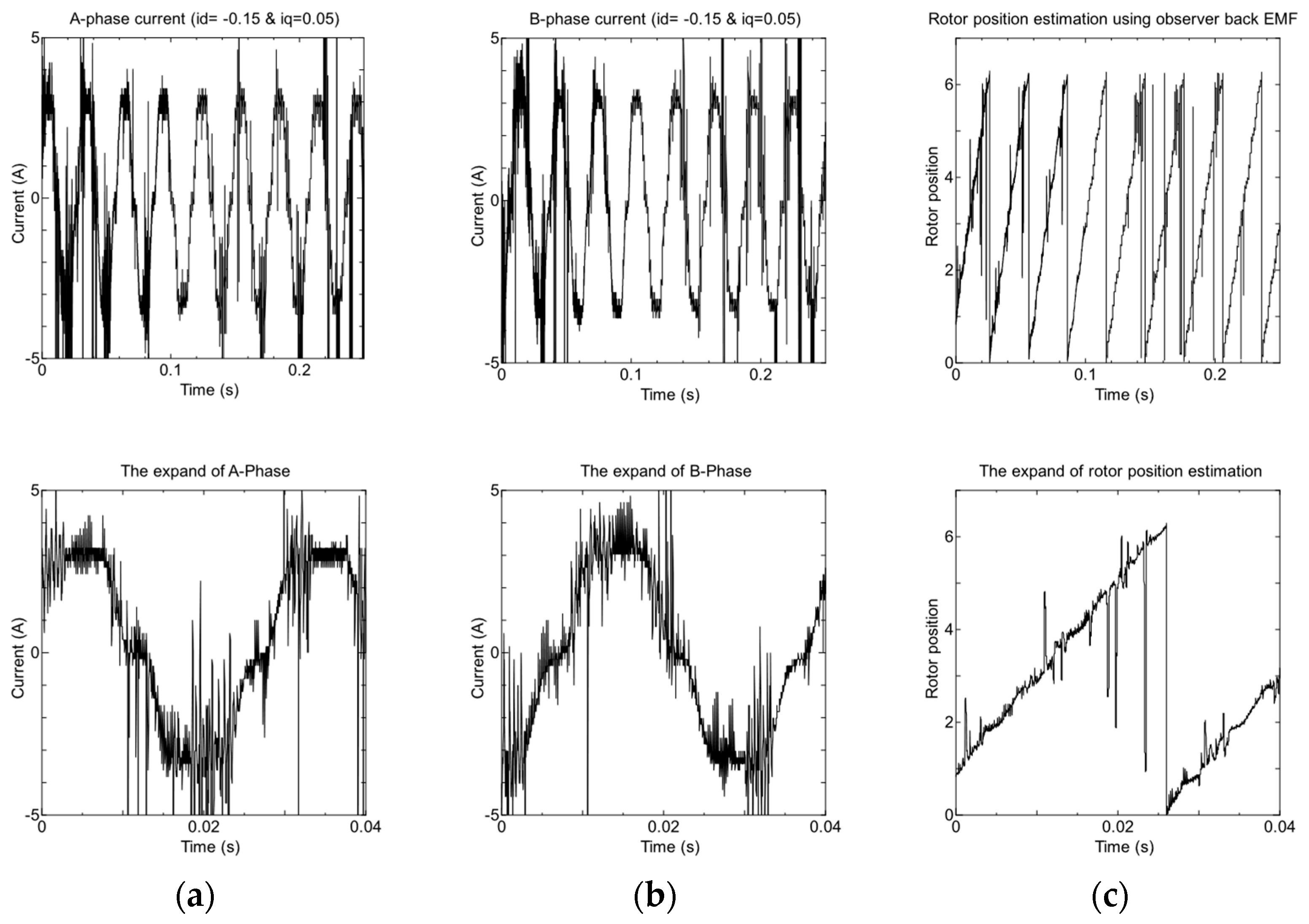
Figure 12.
Observation results for motor control devices using GDC and IR2110 with a capacitance filter in the high and low side: (a) current phase A in 3A; (b) current phase B in 3A; (c) rotor position estimation in 3A.
Figure 12.
Observation results for motor control devices using GDC and IR2110 with a capacitance filter in the high and low side: (a) current phase A in 3A; (b) current phase B in 3A; (c) rotor position estimation in 3A.
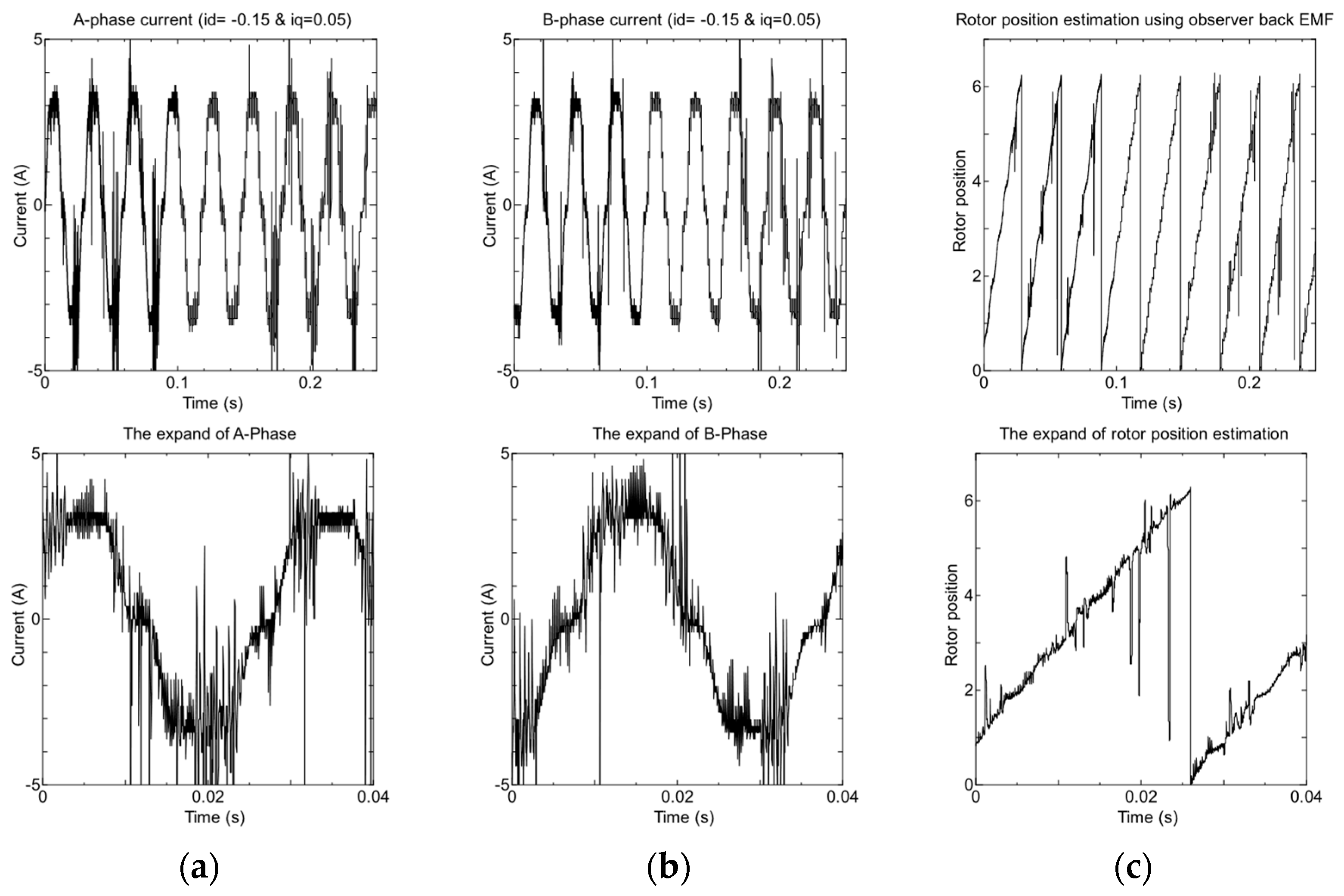
Figure 13.
Observation results of motor control devices using the proposed GDC and IR2110 with the proposed improvement circuit: (a) current phase A in 3A; (b) current phase B in 3A; (c) rotor position estimation in 3A.
Figure 13.
Observation results of motor control devices using the proposed GDC and IR2110 with the proposed improvement circuit: (a) current phase A in 3A; (b) current phase B in 3A; (c) rotor position estimation in 3A.

Figure 14.
Result of noise reduction in motor current signals with different damping values.

Table 1.
Specifications of equipment in experimental setup.
| Components | Specifications |
|---|---|
| DC Power Supply | (PSF-800L), (PW 18-1.3AT) |
| PMSM | DTBL-3518X (4 pole, 185 W, 15A) |
| Current Sensor | PmodISNS20 (ACS722-20A) |
| ADC | ADCS7476 (12 bit with rate conversion 1MSPS) |
| FPGA | ARTY Z7 pynq-20 |
| Memory Hi-CORDER | Hioki 8860-50 |
| PC Interface | Intel(R) Core (TM) i5-7200U |
Table 2.
Comparison of experimental results.
| Type of Configuration | Max. Current Spike | Max. Oscillation Time | Impact of Motor Current | Impact of Rotor Position Estimation |
|---|---|---|---|---|
| Typical configuration | 33% | 4 ms | Large noise spike occurred | |
| Configuration with filter C | <30% | 2 ms | Large noise spike occurred | |
| Proposed configuration | <10% | <1 ms | Large noise spike not occurred | |
Disclaimer/Publisher’s Note: The statements, opinions and data contained in all publications are solely those of the individual author(s) and contributor(s) and not of MDPI and/or the editor(s). MDPI and/or the editor(s) disclaim responsibility for any injury to people or property resulting from any ideas, methods, instructions or products referred to in the content. |
© 2024 by the authors. Licensee MDPI, Basel, Switzerland. This article is an open access article distributed under the terms and conditions of the Creative Commons Attribution (CC BY) license (https://creativecommons.org/licenses/by/4.0/).
Share and Cite
MDPI and ACS Style
Ferdiansyah, I.; Hanamoto, T. Design and Implementation of Improved Gate Driver Circuit for Sensorless Permanent Magnet Synchronous Motor Control. World Electr. Veh. J. 2024, 15, 106. https://doi.org/10.3390/wevj15030106
AMA Style
Ferdiansyah I, Hanamoto T. Design and Implementation of Improved Gate Driver Circuit for Sensorless Permanent Magnet Synchronous Motor Control. World Electric Vehicle Journal. 2024; 15(3):106. https://doi.org/10.3390/wevj15030106
Chicago/Turabian StyleFerdiansyah, Indra, and Tsuyoshi Hanamoto. 2024. "Design and Implementation of Improved Gate Driver Circuit for Sensorless Permanent Magnet Synchronous Motor Control" World Electric Vehicle Journal 15, no. 3: 106. https://doi.org/10.3390/wevj15030106