1. Introduction
Many different techniques have been proposed and used for the measurement of strain over the years. The most widely used technique is resistive strain gauges as at least 80% of strain measurements in stress experiments are performed with them [
1]. These gauges have been used to measure force, pressure, torsion and bending [
2]. A shortcoming of the resistive strain gauges is large strains cannot be measured with this type of gauge, which at most measures up to a single millistrain 10
−3 m/m. Furthermore, variations in ambient temperature will affect strain readings.
Semiconductor strain gauges follow the same principles as resistive strain gauges; however, the resistive material is now substituted by a semiconductor material [
3]. These strain gauges are typically built out of silicon or germanium and have a higher sensitivity to strain. Their breaking strength and elastic strain range is much higher than that of the resistive strain gauges. On the other hand, the temperature range for operation of the semiconductor strain gauges is much smaller (
−40 to
+100
°C) [
3], making it less appealing for high temperature applications.
Photo-elasticity principles are used in strain measurement where an optical mean is utilized in order to determine the strain. These principles primarily apply to the elastic region; however, research has been done to optically measure inelastic strain as well [
1]. Moiré fringe pattern interferometery is another technique that has been used to measure in- and out-of-plane strains, rotations, and curvatures in different materials [
1]. Focused Ion Beam (FIB) Moiré technique was used by Li
et al. [
4] to measure residual strains caused by nano-machining. Large deformations can be measured accurately; however, for small deformation, it requires high-sensitivity moiré interferometry. Another similar method is photo-elastic-coating [
1] where a thin sheet of photo-elastic material is bonded to the material being analyzed. As the material is loaded, the coating deforms with the material and a strain field is developed in the coating. This method is non-destructive and directly measures the strain in the material. Another similar technique utilizes brittle lacquer [
3]. X-ray diffraction has also been used in strain measurement [
3]. It consists of X-raying the area of interest on a structure and using the reflected pattern to determine the strain field and therefore the stress field. It requires that the wavelength of the incident X-rays be of comparable size to the atomic spacing in a crystal and can only be employed on micro-structures having crystal orientations that can diffract x-rays. But as with most strain measurement techniques, x-ray diffraction is only suitable for use in the linear elastic region of deformation.
Acoustic strain gauges [
3] consist of a main strain gauge attached to a steel wire that is plucked by means of a magnet so the natural frequency of the wire can be read. A disadvantage of this type of gauge is that the tension forces on the wire are not taken into consideration and could impact the outcome [
3]. Pneumatic strain gauges use the principle of a pressure increase due to a restriction in the flow stream [
3]. This method is very accurate in the measurement of static and dynamic strains; however, an extensometer is employed to visualize strains which are very nonlinear and requires more complicated configurations to reduce this nonlinearity.
Uttam
et al. [
5] utilized optical fiber to measure micro-strains in the order of magnitude from 0.1 up to 1,000. The advantages of this system include a wide range of micro-strain measured with high agreement with resistive strain gauges and a higher operating life than resistive strain gauges. Unfortunately, in order to use this method the optical fiber has to be embedded in the test specimen and demodulation circuitry has to be employed and a complex signal comparison is required to determine strain. Optical fibers have been used extensively in health monitoring of structures. Che
et al. [
6] achieved micro-strain measurements by means of differential capacitive strain sensors.
All of the techniques mentioned above are suitable for large specimens. When the size of the specimen is reduced to a few millimeters or even less than a millimeter (microscale specimen), these techniques cannot be used effectively. For scales smaller than a few millimeters, better suited techniques are laser extensometers, digital image correlation devices and video extensometers, and in situ testing using Scanning Electron Microscope.
Digital image correlation (DIC) has been one of the key techniques for strain measurements [
7] at microscale. Difficulties involved with DIC and video extensometer techniques are surface requirement and extensive post processing steps. Additionally the equipment are relatively more expensive. Laser extensometer is another technique that has been used in small scale. Again this technique requires certain surface finish or marking of the surface. Combination of digital image correlation, change in surface topology using atomic force microscopy, and integrated capacitive gauges were used by Espinosa
et al. [
8]. Another method that has been studied for microscale measurement is measurement through the utilization of a magnetoelastic microtransformer. This approach was taken by Amor
et al. at the Institute for Microtechnology, Hanover University in Germany [
9]. They utilized a magnetoelastic material in order to take advantage of the Villari effect. The Villari effect describes the change in permeability of a magneto-elastic material as it is subjected to deformation. Only compressive strains were reported in this study. Another research for strain measurement at microscale on magnetoelatic microtransformers was conducted by a joint team of researchers from the Slovak University of Technology, the Institute of Physics in the Czech Republic and Slovakia and the Istituto Elettrotecnico Nazionale Galileo Ferraris in Italy where they determined the effect of ambient temperature on the strain measurements [
10].
Several other devices and materials have been developed that can be used as strain gauges such as the device developed by Lin
et al. [
10] Mamin
et al. [
12], Herbert
et al. [
13], Tata
et al. [
14] and Anand and Mahapatra [
15]. These devices or materials need to be integrated with specimens in order to measure the strains. Still problem exist for measuring strains in specimens that may even be smaller than these strain gauges.
Many of the techniques mentioned here are not applicable for specimens that are smaller than the strain gauge itself. Some methods require extensive equipment and large amount of post processing in order to be used at microscale where the sample size is between approximately 0.01 and 1 millimeters. A new technique is proposed for its simplicity and applicability for microscale application. This technique requires small amounts of post processing making it suitable for cyclic and fatigue testing of material at smaller scales. Electroactive (piezoelectric) concepts are utilized to measure elastic and plastic strains in a microscale specimen. Knowing strain, other material properties such as Young’s modulus can be determined for unknown materials. The use of this technique is particularly applicable to small scale because lower levels of voltage are required (As the electric field is defined as voltage/distance, for creating an electric field of 1,000 v/m, the required voltage for a piezoelectric thickness of 1 cm is 10 v, but this required voltage reduces to 1 V for a thickness of 1 mm) to create a large electric field over thinner piezoelectric member.
At the microscale and smaller, the deformation of piezoelectric members subjected to a reasonably small electric field is far more noticeable. This scale allows the relative deformation of a system containing piezoelectric members and test materials to be quantified and recorded in a much simpler manner. Using a system with two piezoelectric members with a test material in between allows strain measurements to be made given the measurements of only the applied voltage in one piezoelectric member and the induced voltage in the other.
2. Strain Measurement Using Piezoelectric Sensor
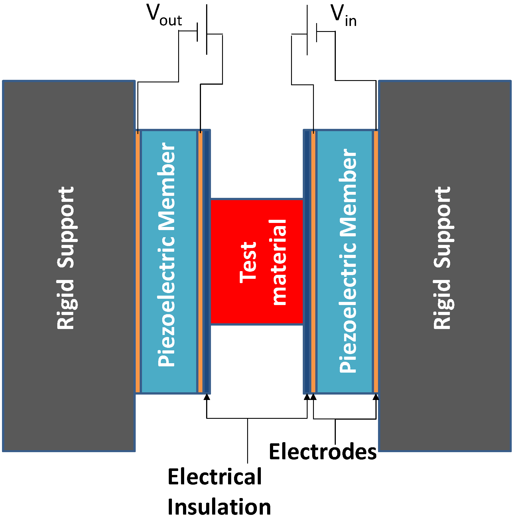
The test apparatus consists of two piezoelectric members (usually plates) which constrain the specimen from both sides and are constrained within a very rigid frame as seen in
Figure 1.
Figure 1.
The dual piezoelectric-actuator-sensor apparatus.
Figure 1.
The dual piezoelectric-actuator-sensor apparatus.
As input voltage is applied on the first piezoelectric member, it deforms. Since the structure is constrained within the rigid frame, the total deformation of the system consisting of both piezoelectric members and the test specimen is zero. It is unrealistic to assume that the frame will be perfectly rigid, but it is a small matter to determine its compliance and adjust the strain and output voltage results accordingly. The choice of frame material is important though, since piezoelectric materials generally are very stiff (the material described in the following analyses has an elastic modulus of 119 GPa). It is necessary to choose a material stiffer than the piezoelectric material used in the strain sensor. Steel, silicon and sapphire are all reasonable choices, particularly since this sensor is only fit for use at the microscale and the amount of supporting material required is relatively small.
With the application of the input voltage to the first piezoelectric member, force is developed in the first piezoelectric member and transferred through the test material to the second piezoelectric member, inducing some deformation in the second piezoelectric member. This deformation is directly proportional to the stiffness of the test material in the linear elastic region. Deformation in the second piezoelectric member can be determined by measuring the output voltage signal. If the stiffness of the test material changes, the force developed inside the structure will change and as a result the output voltage will change. This concept can be used to determine the material properties of the test material in addition to measuring the strain developed in the test material. PZT and other piezoelectric materials are known to have considerable hysteresis in displacement versus voltage. This hysteresis loops can be eliminated using closed loop piezoactuator or using hysteresis inverse models [
17].
3. Theoretical Analysis
3.1. Determining Sample’s Elastic Modulus
Piezoelectricity is a linear phenomenon that relates linear elasticity with electric charge 19. Many applications have been developed for the use of piezoelectric materials. Among them we have acoustic emission detectors, medical ultrasonic transducers, piezoelectric actuators and buzzers and piezoelectric transformers supplying high voltage [
18]. One advantage of piezoelectric material is their high yield stress (45–55 MPa) which provides a wide elastic range which is utilized in this new technique. The governing equations for piezoelectricity in matrix form are:
where
ε (
dimensionless) is the (6 × 1) strain vector,
D (
C/m2) is the (3 × 1) electric displacement vector,
σ (
Pa) is the (6 × 1) stress vector,
E (
V/m) is the (3 × 3) applied electric field,
eσ (
F/m) is (3 × 3) dielectric permittivity,
d (
C/N) is the (3 × 6) piezoelectric constant, and
SPZ (
Pa−1) is the (6 × 6) elastic compliance matrix. The piezoelectric constant,
, defines electric displacement per unit stress in a constant electric field, and its transpose,
dT, defines strain per unit field at a constant stress. The well known transformation between elastic compliance and elastic stiffness is shown in Equation 3.
As mentioned before, the strain measurement system consists of two piezoelectric plates with a sample of test material in between. The two piezoelectric members are denoted as segments 1 and 3, while the test material between them is denoted as 2. The whole system is rigidly constrained at the outer edges of the piezoelectric plates, allowing the following relationship to be used:
For this calculation, all three plates have equivalent dimensions in all directions (length
l, width
b, and thickness
t). The stress and resulting strains of interest occur only in the axial direction (
z) allowing the displacement relationship of Equation 4 to be further developed into the strain relationship shown by Equation 5.
Furthermore, since the plates all have the same cross-sectional areas, the stresses developed in each will be equivalent (see Equation 6).
Voltage,
V, is applied across the first piezoelectric material (segment 1), and the electric field it induces in the z-direction is described as:
Similarly, the electric field induced in the second piezoelectric material (segment 3) is described in terms of the voltage measured across the plate, as shown in Equation 8.
Substituting Equation 7 into Equation 1 and using only the terms that directly describe the materials response in the z-direction, the axial strain is described in terms of voltage applied and stress induced by Equation 9.
The strain, and therefore stress, induced in the second piezoelectric material (segment 3) is the most difficult to describe. Piezoelectric plates can be likened unto parallel plate capacitors, and the first step in determining the voltage across a capacitor is defining the generated electrical charge. Since the deformation in this segment is purely due to the stress induced in the system, the electrical displacement described by Equation 2 is reduced, in the z-direction, to [
20]:
The charge generated is related to this electrical displacement by
And the voltage induced in the third segment by:
The capacitance of a piezoelectric sheet is described by
So by substituting Equations 11 and 13 into Equation 12, the voltage induced in the third segment is described as shown in Equation 14.
Since the output voltage is already known in this strain measurement system, Equation 14 is solved for stress:
Using Hooke’s law, the strain in the third segment is described in Equation 16.
Note that the strain in the first segment (Equation 9) has an equivalent stress term in it. So it is further expressed as:
Substituting Equations 16 and 17 into Equation 5, solving for the strain in the second segment, and using Hooke’s law yields Equation 18:
Young’s Modulus,
, is the inverse of the compliance term shown and can be determined by substituting Equation 15 into Equation 18, as shown in Equation 19, and solving for
, as shown in Equation 20:
This process allows for strain and elastic modulus of any isotropic test material to be determined when only the voltage applied to the first piezoelectric segment and the voltage induced on the second piezoelectric segment are known.
3.3. Determining Coefficient of Thermal Expansion
Similarly to determining the plastic tangent modulus, the coefficient of thermal expansion (CTE), can be determined with this strain apparatus. For this derivation it is assumed that the temperature load will not induce a stress above the yield stress of either the piezoelectric pieces or the test material. Additionally, Young’s modulus of the test material must be known before the CTE can be determined.
The only load applied is the thermal load, so now both piezoelectric segments are treated as sensors, and it is assumed that equivalent electric fields, and thus equivalent voltages, will be induced in both. Also, the rigid supports are also treated as though they have an infinitesimal CTE (or they are fixed from the side attached to the specimen and free to deform from other side) and deformation due to the supports is neglected. The same geometric equivalencies are also used. First the sum of the strains originally defined by Equation 5 is rewritten in Equation 24 to account for the strains in the piezoelectric pieces being equivalent.
These strains are redefined for both the piezoelectric material and the test material in terms of their respective CTEs,
, by Equations 25 and 26 where
is the thermal load. Equation 25 also shows the strain in the piezoelectric materials in terms of the induced voltage.
A stress balance is competed by substituting Equation 26 and the first part of Equation 25 into Equation 24, as shown in Equation 27. Equation 28 is the result of solving Equation 27 for stress.
Similarly, Equation 26 and the second part of Equation 25 are substituted into Equation 24 yielding Equation 29.
Substituting Equation 28 into the stress term here and solving for the CTE of the test material yields Equation 30.
3.4. Predicting Output Voltage for known Sample Properties
Since this is a theoretical analysis, the output voltage is unknown in all cases. It is more useful to assume some material properties and predict the output voltages. These voltages can then be used for calibration of the sensor and to determine the characteristic behavior of the sensor when the properties of the test sample are known. The derivations are exactly the same, but instead of solving for the desired material property, the output voltage is solved for instead. So for the analysis of the elastic modulus, Equation 19 is solved for
instead of
, and the solution is shown in Equation 31.
For the plastic modulus analysis, Equation 23 is manipulated so the output voltage can be predicted in terms of the assumed material properties as shown in Equation 32.
And finally for the CTE analysis, Equation 30 is solved for output voltage as shown in Equation 33.
These relations provide an excellent way to compare the analytical solution to a solution developed using finite element analysis. Both are done using assumed material properties.
4. Finite Element Analysis
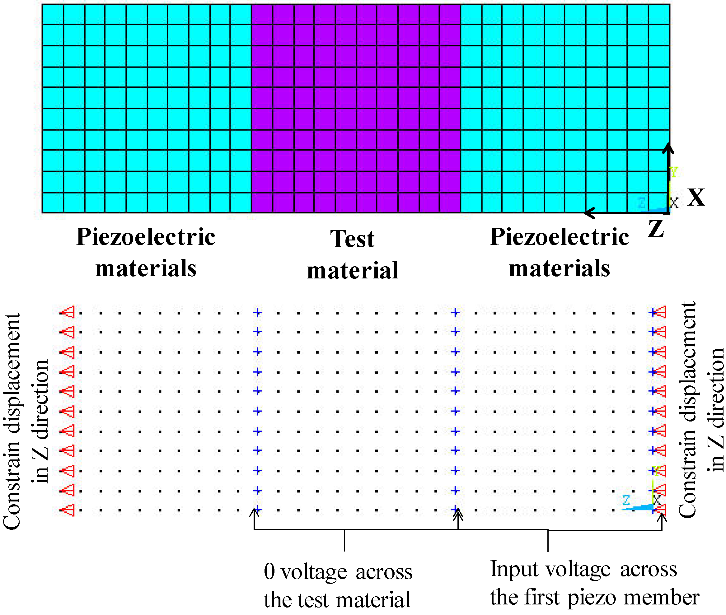
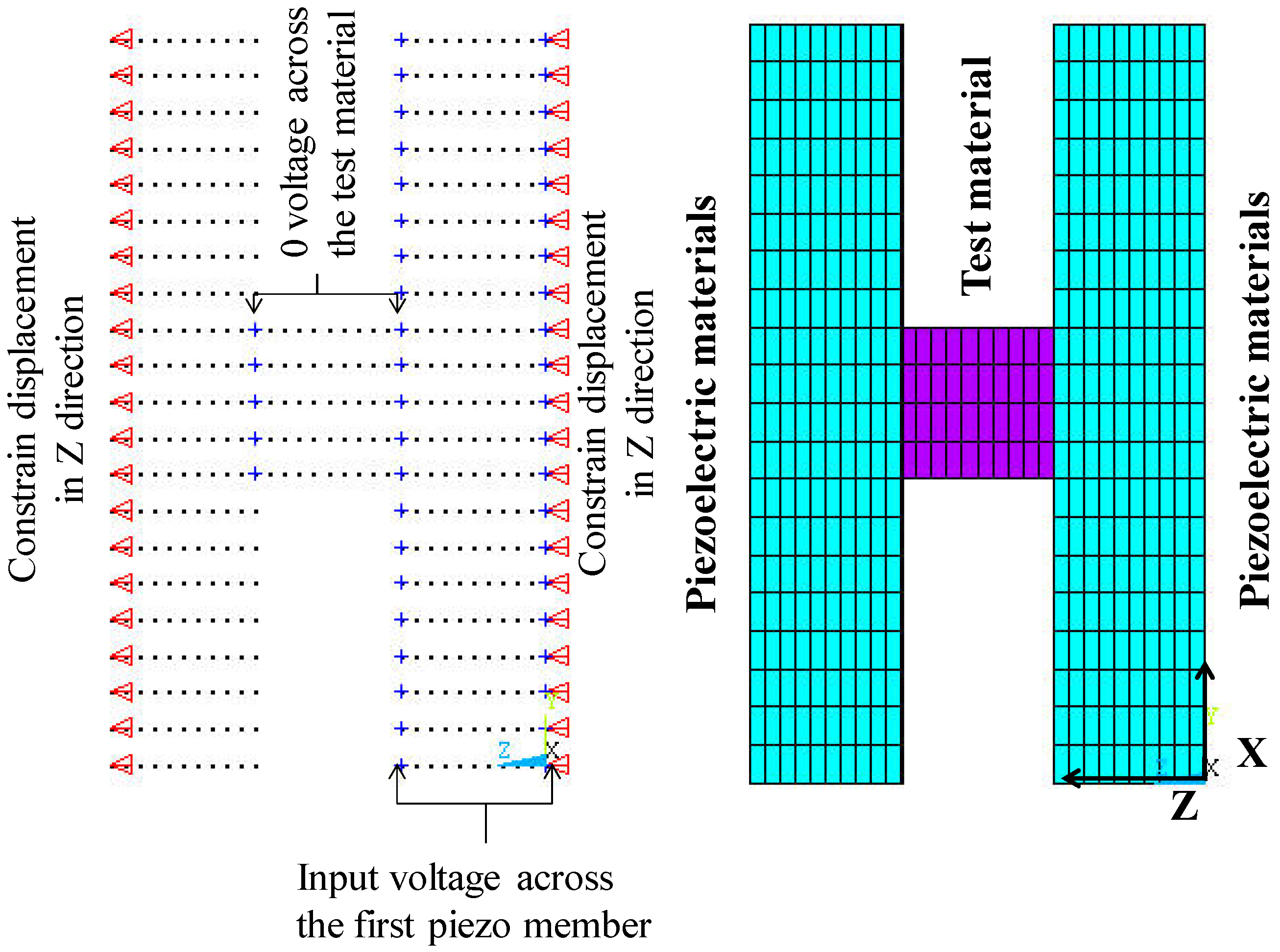
A finite element (FE) model is developed and conducted using ANSYS to predict output voltage given an input voltage and known sample properties. The results are used to correlate the elastic modulus of the test specimen to the induced output voltage, allowing a comparison to be made with the analytical predictions. In addition to the linear analysis, where the sample’s modulus of elasticity or the induced output voltage can easily be predicted, a non-linear analysis of test specimen’s plastic deformation is conducted to investigate the capability of the strain sensing system in indicating plastic behavior. SOLID5 elements are used to model the piezoelectric segments as it is a coupled-field solid element with capabilities in thermal, magnetic, electrical, structural and piezoelectric analysis. The test material is modeled with SOLID185 elements, because it has the capability to model non-linear and plastic behavior.
Figure 1 describes the geometry, boundary conditions, and axes orientations modeled in ANSYS.
The piezoelectric material used in the model is part of the class 4mm crystals, lead zirconate titanate
and is a piezoelectric ceramic that exhibits substantial deformation when subjected to an electric field. Its crystal structure is such that the x- and y-axes are symmetric, reducing the number of material constants in a way consistent with transversely isotropic materials. From all the piezoelectric ceramics available, PZT-5H is chosen due to its large piezoelectric constant in the z-direction,
, which causes a higher z-deformation when the electric field is applied in the z-direction. The piezoelectric constant, elastic compliance, dielectric permittivity, and CTE of PZT-5H used in the finite element analysis are shown in matrix form in Equations 34, 35, 36, and 37 respectively.
Additionally, since all material properties must be defined before using finite element to model anything, a test material is defined using the material properties shown in
Table 1. These properties are also used in the theoretical comparisons to the FE results.
Table 1.
Material properties of test specimen used for test case comparisons.
Table 1.
Material properties of test specimen used for test case comparisons.
| Modulus of Elasticity | 100.0 GPa |
| Poisson’s ratio | 0.3 |
| Yield stress | 1.0 MPa |
| Tangent modulus | 5.0 GPa |
The FE model, mesh, boundary conditions, and applied voltage load are shown in
Figure 2. For the initial configuration, the cross sectional area of both the test specimen and piezoelectric materials are equivalent (1 mm × 1 mm). The thickness of the piezo members and the specimen are all 1mm. The free ends of the piezoelectric material are constrained from displacement, the electric field within the test material is forced to be zero, and the voltage is applied across the first segment of piezoelectric material.
Figure 2.
Finite element model of the strain sensing system where the piezoelectric segments have cross-sectional areas equivalent to the test segment, with loads and constraints shown.
Figure 2.
Finite element model of the strain sensing system where the piezoelectric segments have cross-sectional areas equivalent to the test segment, with loads and constraints shown.
Now, the induced voltage on the second piece of piezoelectric material is predicted. The results are compared to those of the theoretical analysis of the output voltage in the next section.
5. Comparison of Analytical and Finite Element Results
Both elastic and plastic analyses are conducted in ANSYS using the test material properties and the piezoelectric properties described in previous section. The strain measurements and voltage responses generated by each are compared below.
5.1. Strain Measurement
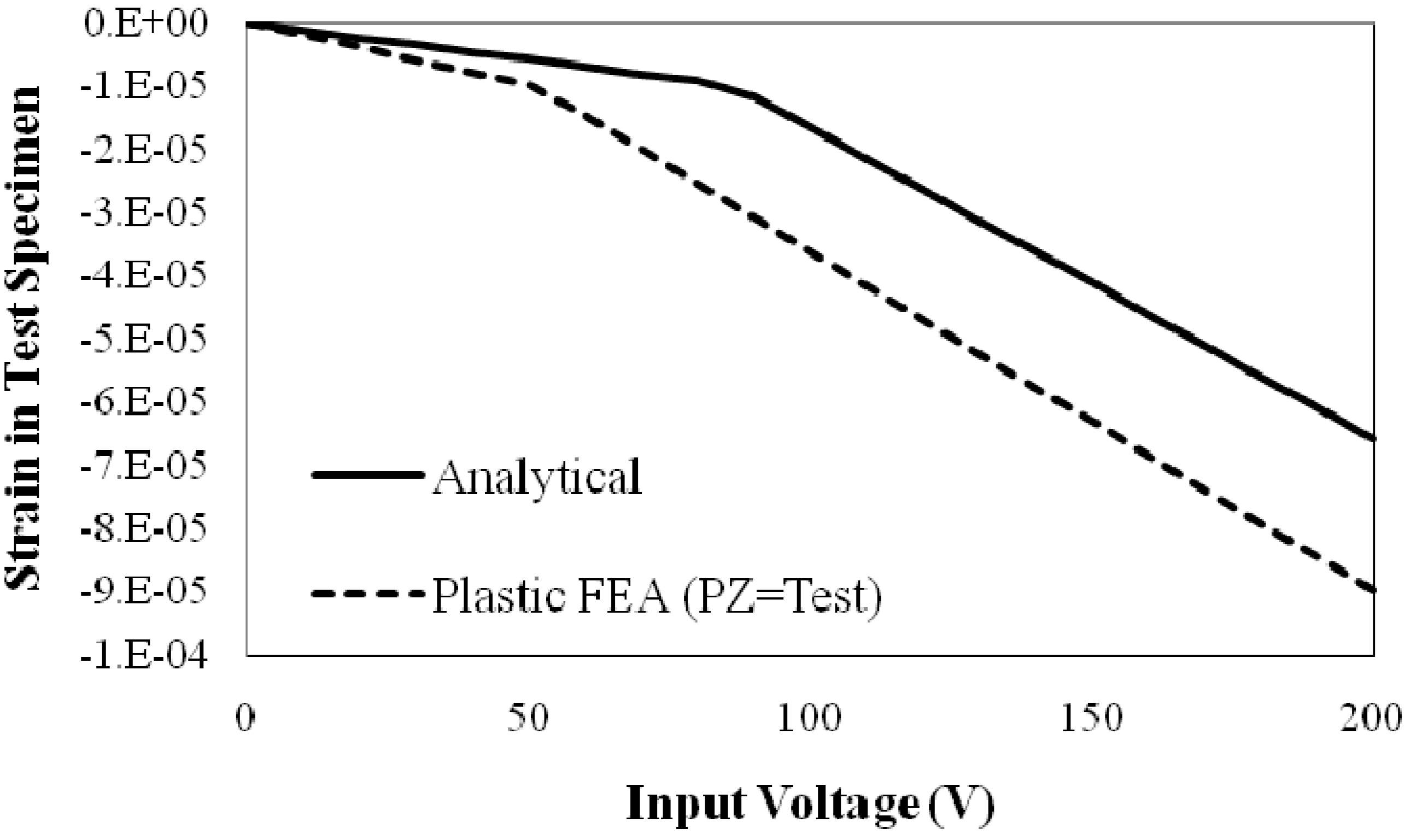
Since this apparatus is primarily a strain measurement device, strains in the test specimen generated analytically and using finite element techniques are shown first in
Figure 3. Both elastic and plastic deformations are accounted for in this figure. The analytical and finite element solutions do differ significantly, but they follow the same overall trend. These curves are very reminiscent of stress strain curve, which is expected since the stress levels in the strain sensing system are directly proportional to the voltage applied to the first piezoelectric member. The difference in yield point is the most obvious discrepancy between the two curves and is likely attributed to localized deformations in the finite element model. Proper calibration of the strain sensing device is necessary to account for this discrepancy.
Figure 3.
Comparison of strain measurements generated analytically and with finite element.
Figure 3.
Comparison of strain measurements generated analytically and with finite element.
5.2. Elastic Analyses
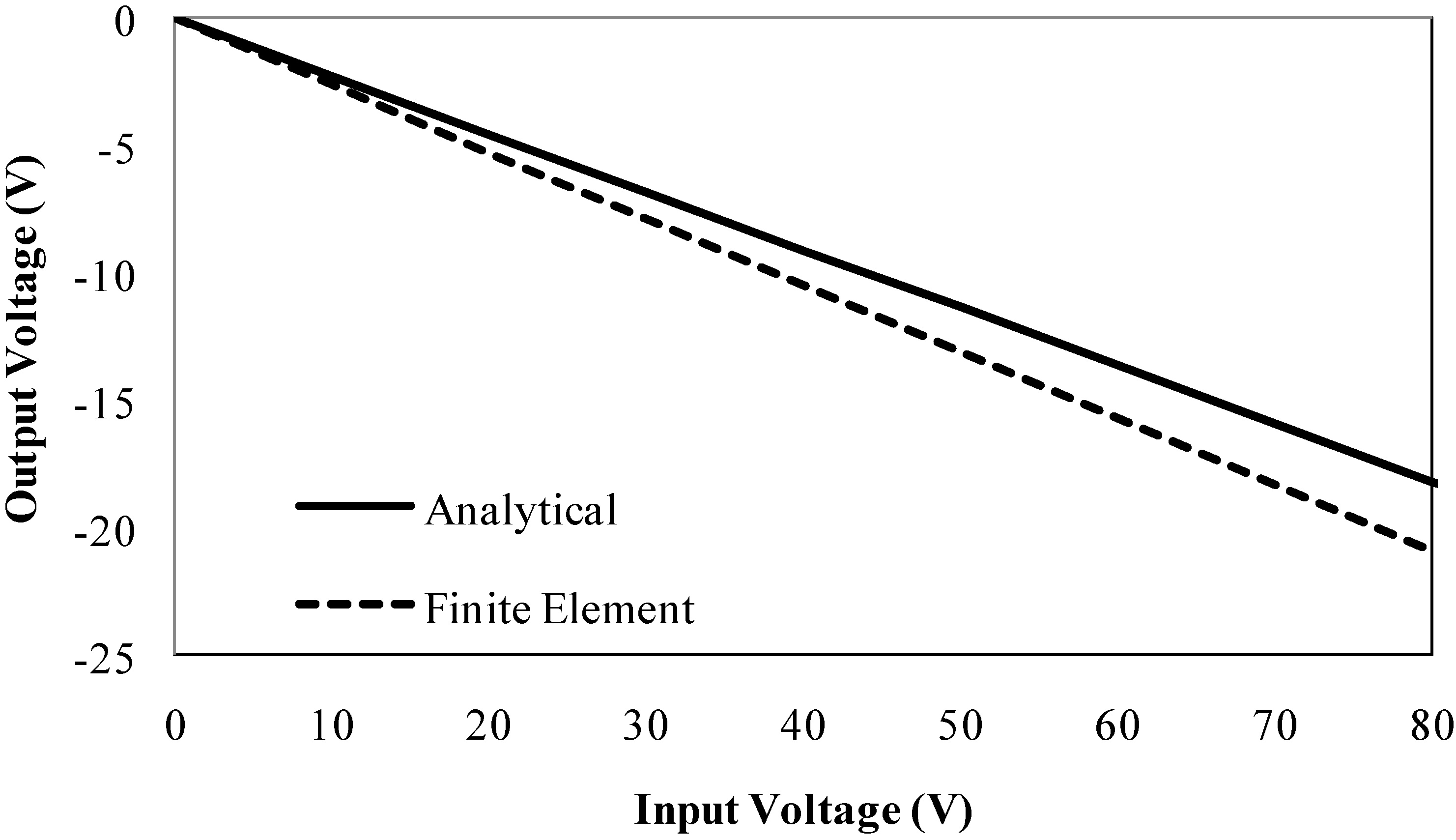
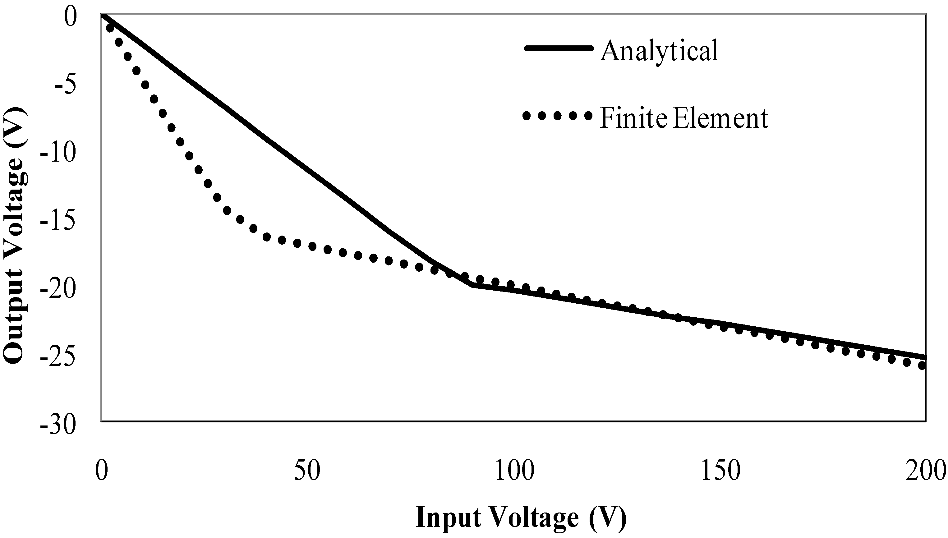
Figure 4 shows the differences between the analytical output voltages and the finite element model’s output voltages for a range of applied input voltages. For this FE analysis, only the elastic properties of the test sample are used, and induced voltages were only measured while the stresses were below the yield strength of the test material. All induced voltage responses were generated entirely in the elastic regime, and the linear behavior of both confirms this.
Figure 4.
Comparison of induced voltage responses generated analytically and with finite element within the elastic regime
Figure 4.
Comparison of induced voltage responses generated analytically and with finite element within the elastic regime
The two solutions are constantly 15% different than one another, indicating that the solutions are proportional, and that within the elastic region the modulus of elasticity can be determined from the strain sensor as long as the proportional relationship between output voltage and elastic modulus is calibrated correctly.
5.3. Plastic Analyses
Figure 5 is a comparison induced voltage predicted by the analytical and FE solutions for a range of applied voltages. Here the plastic properties of the test material are used in ANSYS and defined using a bilinear hardening law. Both analytical approach and finite element are able to determine the yield strength and reasonable tangent modulus. Bi-linear behavior is clearly shown. This model was used for simplicity, but from the results we predict that device is capable of detecting the non-linear plastic behavior by a similar non-linear output voltage. Note that in this case, the Finite Element solution severely over-predicts the magnitude of the induced voltage, relative to the analytical solution. This is attributed to the edge effects on stress and deformation as well as highly localized plasticity that served to stiffen the material more than would be realistic. To avoid this discrepancy between the finite element and analytical model, several modifications to design and configuration are proposed and are presented in following sections.
Figure 5.
Comparison of induced voltages generated analytically and from finite element models using a bilinear hardening relationship for plasticity.
Figure 5.
Comparison of induced voltages generated analytically and from finite element models using a bilinear hardening relationship for plasticity.
6. Design Modification
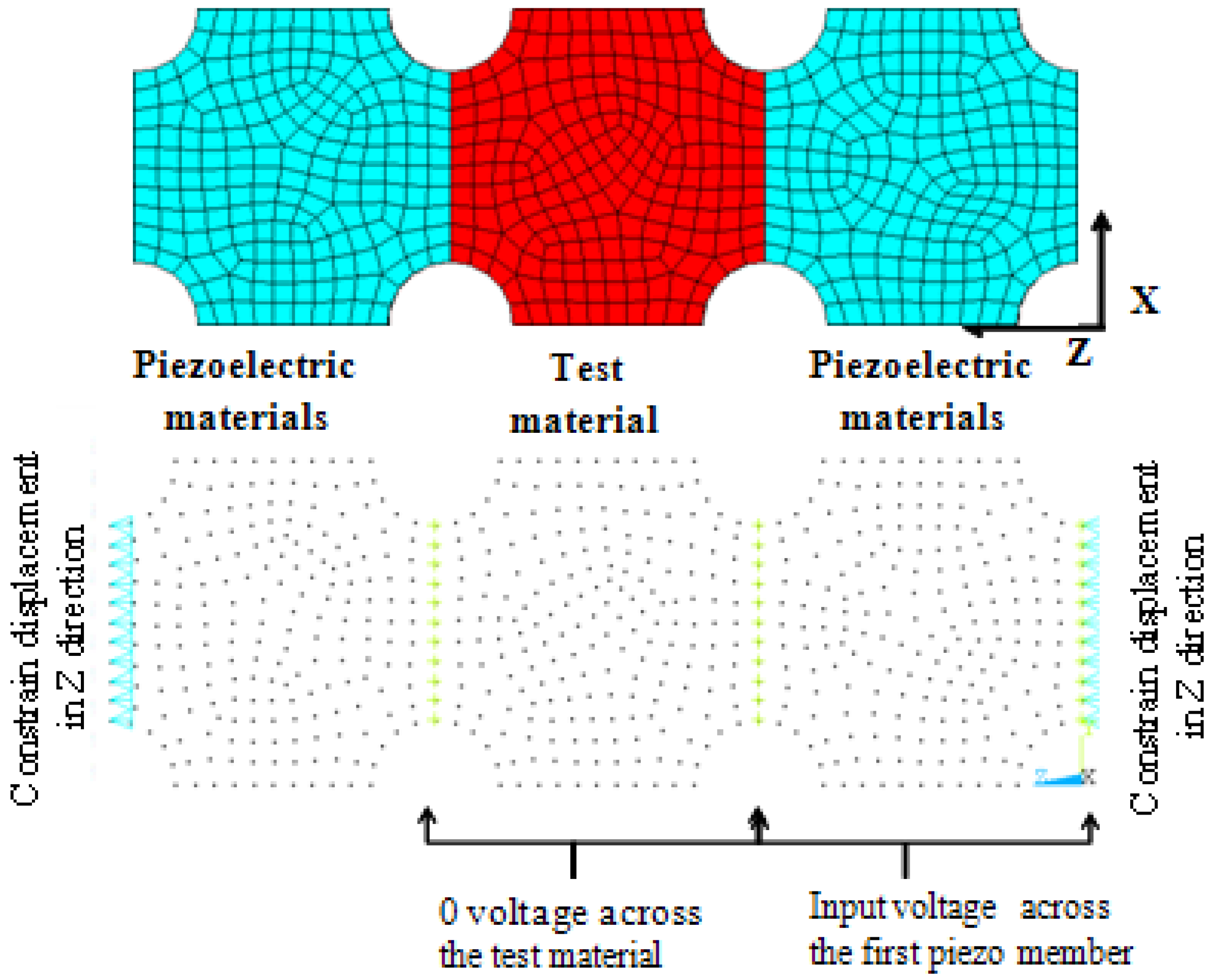
The discrepancies observed between the finite element and the analytical models were caused by the edge effect and concentrated stress that causes plastic deformation at the edges. The plastic deformation at the edge reduces the average deformation in the specimen, making it virtually stiffer which causes the larger output voltages. Several modifications are proposed to avoid severe plastic deformation at the edges. First, in an attempt to create a much more uniform deformation in the test segment that is free of edge effects, a new design is proposed in which the piezoelectric segments are built with cross-sectional areas 25 times greater than the test segment. The thicknesses of the piezoelectric materials and test specimen still remain the same.
Figure 6 shows the finite element model, mesh, boundary conditions, and applied voltage load. The analytical model remains the same for both the initial configuration using equivalent cross sections and the new cross section using non-equivalent cross section area. Due to small thicknesses of piezoelectric members, the stress will remain concentrated mostly within the interface cross section area and does not dissipate to larger piezo electric member area. The thicknesses of all the segments are equal (
t1 =
t2 =
t3), the lengths and widths of each segment are equal (
l1 =
b1;
l2 =
b2;
l3 =
b3), and the piezoelectric segments have the same dimensions as each other.
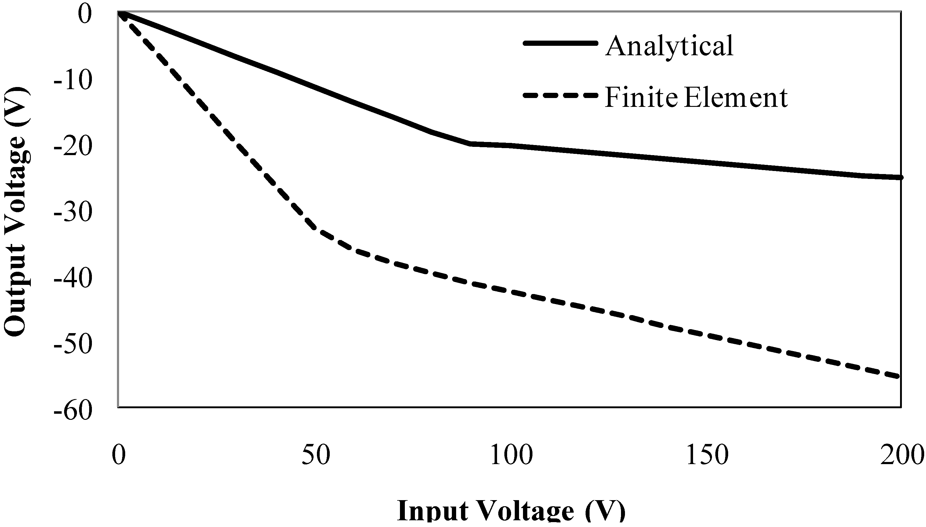
Surprisingly, the FE solution using larger piezoelectric plates produces results that deviate from the analytical solution in a different manner, as shown in
Figure 7. The elastic region now does not confirm with the analytical solution. However, analytical and finite element models both predict almost equivalent values for the tangent modulus. This deviation from the analytical model in the elastic region is reasoned to be due to deviation from uniformity of stress in z-direction in the piezoelectric material. Since the area of specimen is now much smaller than the piezoelectric material, the stress in more concentrated in the center of the piezoelectric segments. Therefore, the FE solution deviates from the initial assumption of uniform stress in the z-direction used for the analytical analysis.
Figure 6.
Finite element model of the strain sensing system where the piezoelectric segments have larger cross-sectional areas than the test segment, with loads and constraints shown.
Figure 6.
Finite element model of the strain sensing system where the piezoelectric segments have larger cross-sectional areas than the test segment, with loads and constraints shown.
Figure 7.
Comparison of the results for analytical and finite element solution with larger piezoelectric members when plasticity is included
Figure 7.
Comparison of the results for analytical and finite element solution with larger piezoelectric members when plasticity is included
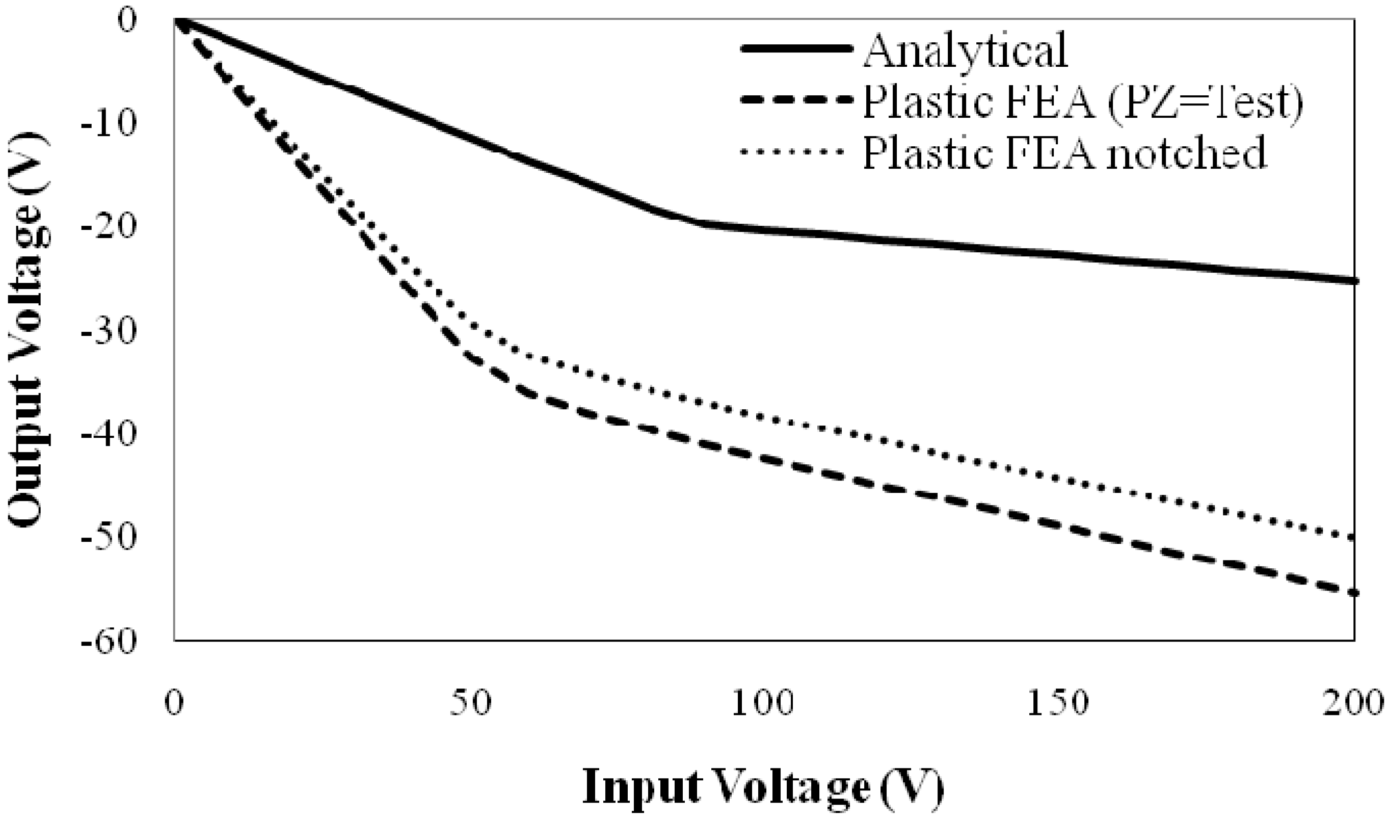
Another design modification consists of adding notches to the segments, as shown in
Figure 8. These notches should serve to reduce the effects of Poisson’s ratio in the 3-D FE model. A solution more similar to the analytical solution where all stress, strain, and electric fields are limited to the principle axis is obtained.
Figure 8.
Finite element model of the strain sensing system where the segments are notched, with loads and constraints shown.
Figure 8.
Finite element model of the strain sensing system where the segments are notched, with loads and constraints shown.
Figure 9 compares the analytical solution and the original FE solution to the notched FE solution for an inelastic solution. Adding the notches to the segments does serve to bring the FE solution closer to the analytical solution, and with proper notch design, the relative gains could increase even more.
Figure 9.
Comparison of the analytical and FE results using equivalent segments, and equivalent notched segments when plasticity is included.
Figure 9.
Comparison of the analytical and FE results using equivalent segments, and equivalent notched segments when plasticity is included.
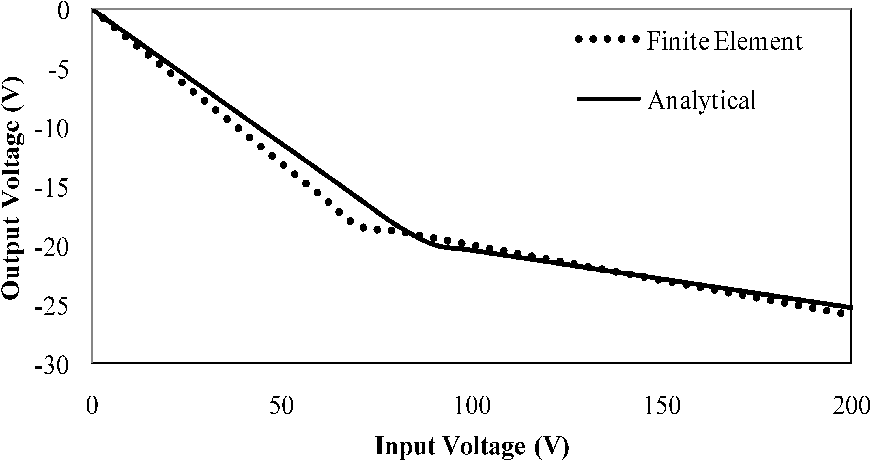
The FE model that utilizes equivalent segments agrees very well with the analytical solution in the elastic regime. Also, the FE model using larger piezoelectric pieces emulates the analytical solution in the plastic regime almost exactly. Using the purely elastic FE model with equivalent segment geometries and the purely plastic portion of the plastic FE model with larger piezoelectric segments, the analytical solution is shown to be a very good approximation. This comparison is shown in
Figure 10. Though the slopes in both the elastic and plastic regions are slightly over predicted in the Finite Element solution (relative to the analytical solution), the level of agreement is still profound. Of course this indicates that in order to get the most accurate results, the strain sensing system should be set up differently for elastic tests and inelastic tests.
Figure 10.
Comparison of induced voltages generated analytically and from both the elastic and plastic Finite Element models.
Figure 10.
Comparison of induced voltages generated analytically and from both the elastic and plastic Finite Element models.
7. Voltage Characteristics and Predicting Material Properties
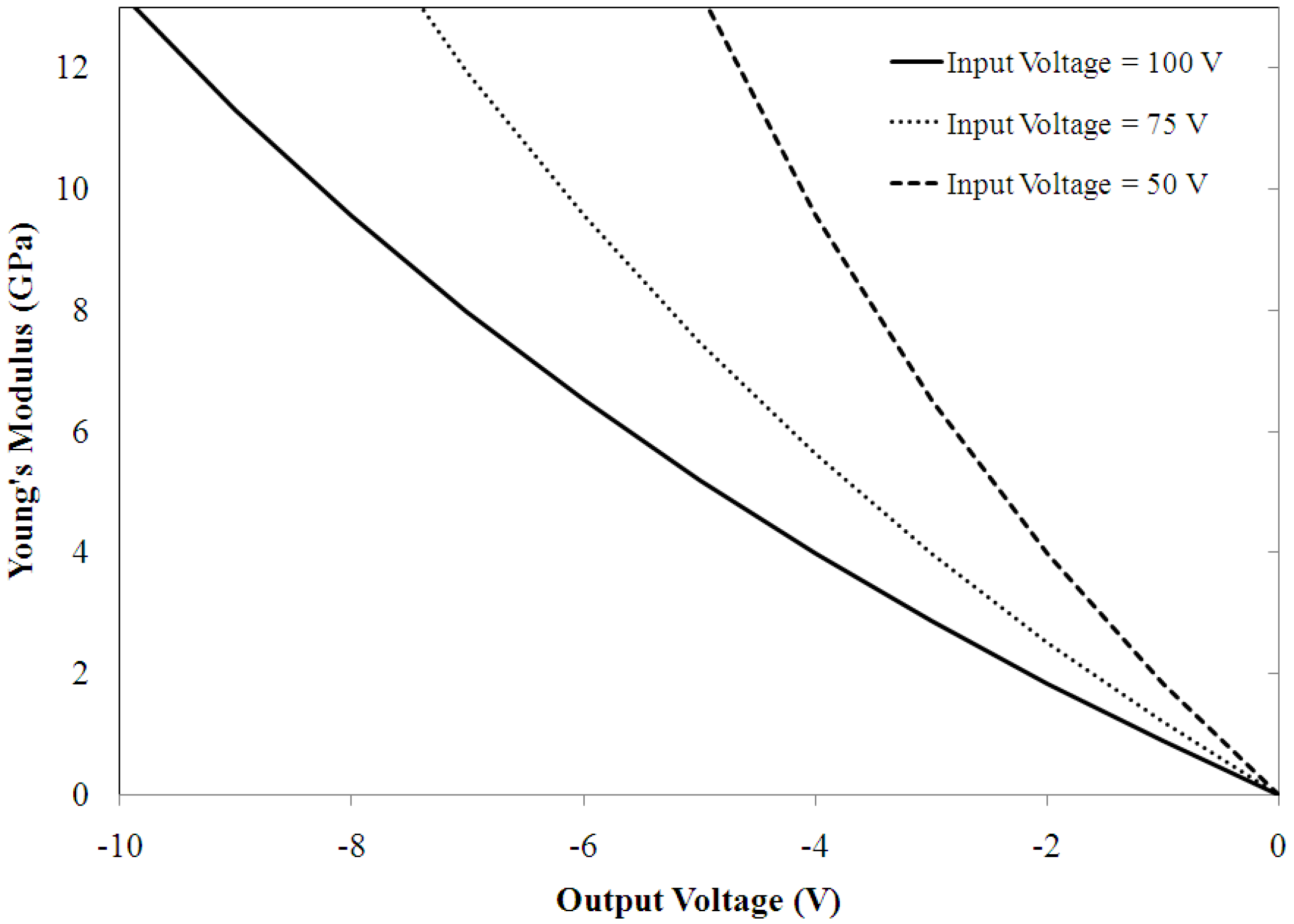
7.1. Elastic Characteristics
The analytical model is used to predict the Young’s modulus of the test material for applied voltages of
,
and
for a range of output voltages. Theoretically there is a voltage induced by a strain in the third segment that will balance the strain resulting from the applied voltage. This balance indicates a rigid test specimen having an infinite elastic modulus and occurs when
V3~−0.28 V1. Values of induced voltage near or above this value are unrealistic as there is no material with an infinite elastic modulus. Furthermore, when the output voltage exceeds 10 percent of the input voltage, the response of the elastic modulus become more non-linear, indicating an even lower limit of applicability. Since the test material is assumed to be far less stiff than the piezoelectric material, this limit on output voltage is reasonable. The characteristic curve shown in
Figure 11 is limited to elastic moduli under
13 GPa that may realistically be tested given the piezoelectric properties of this strain sensor system and only shows the voltage response of the second piezoelectric member given these constraints on the range of testable specimens. Within this range the response is linear which helps with calibration of the device.
Figure 11.
Predicted test material’s elastic modulus relative to the induced voltage and applied voltage.
Figure 11.
Predicted test material’s elastic modulus relative to the induced voltage and applied voltage.
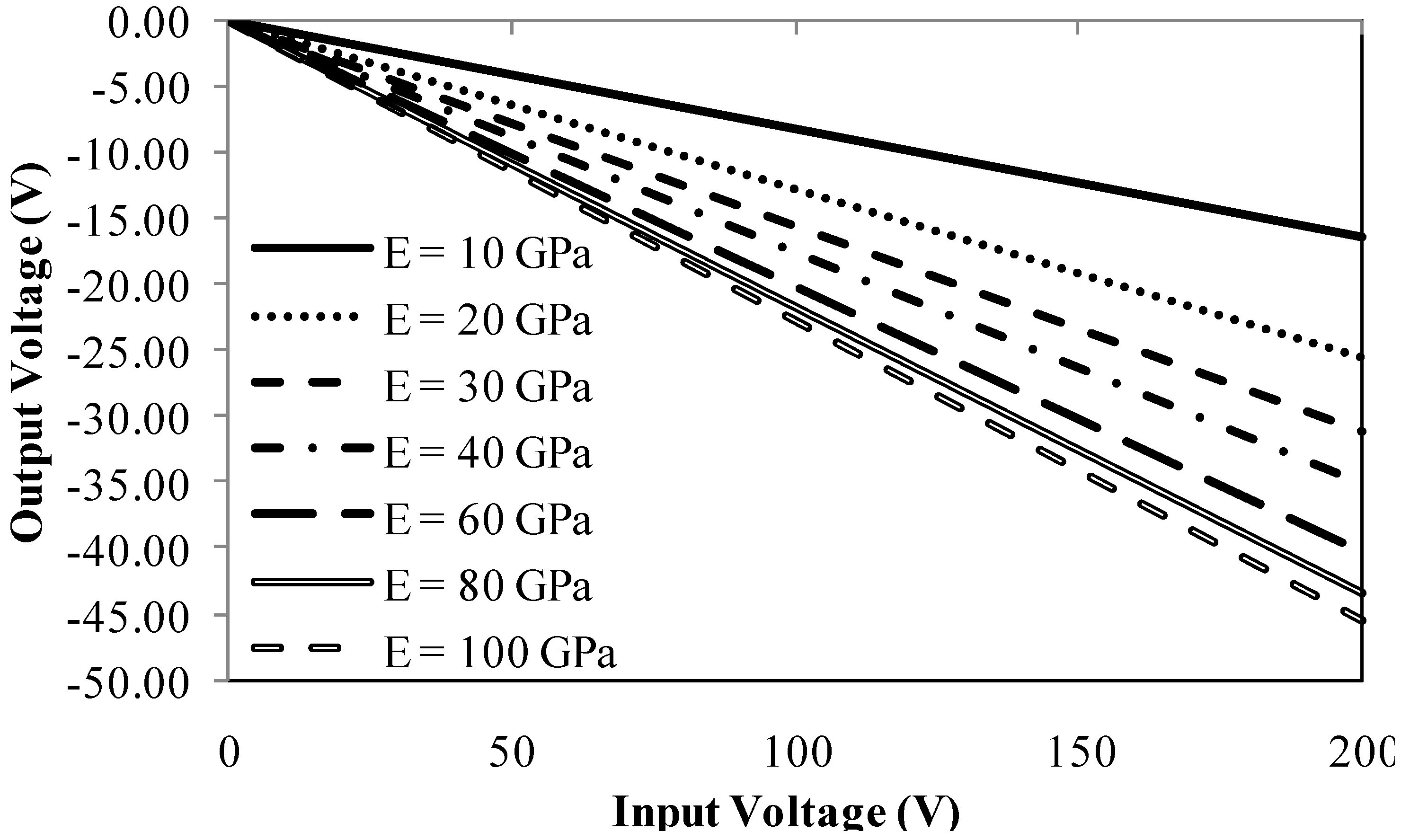
Since any voltage may be input to the strain sensing system, it is necessary to characterize how the output voltage changes for specific materials.
Figure 12 shows the linear behavior of output voltage as input voltage is increased for a range of elastic moduli. This linear response of output voltage is expected, and is directly proportional to the elastic modulus. Note that the range of elastic moduli exceeds the 15 GPa limit described relative to output voltage in
Figure 11. It is interesting to see that despite there being a non-linear response of elastic modulus relative to output voltage given a constant input voltage, the non-linearity disappears in the output voltage when the elastic modulus is held constant and the input voltage varied. This indicates that the limit on elastic modulus of 15 GPa is not a firm limit and that this strain measurement device will still work as long as the elastic modulus of the test material is lower than that of the piezoelectric material.
Figure 12.
Induced voltage resulting from applied voltage for a range of test specimen properties.
Figure 12.
Induced voltage resulting from applied voltage for a range of test specimen properties.
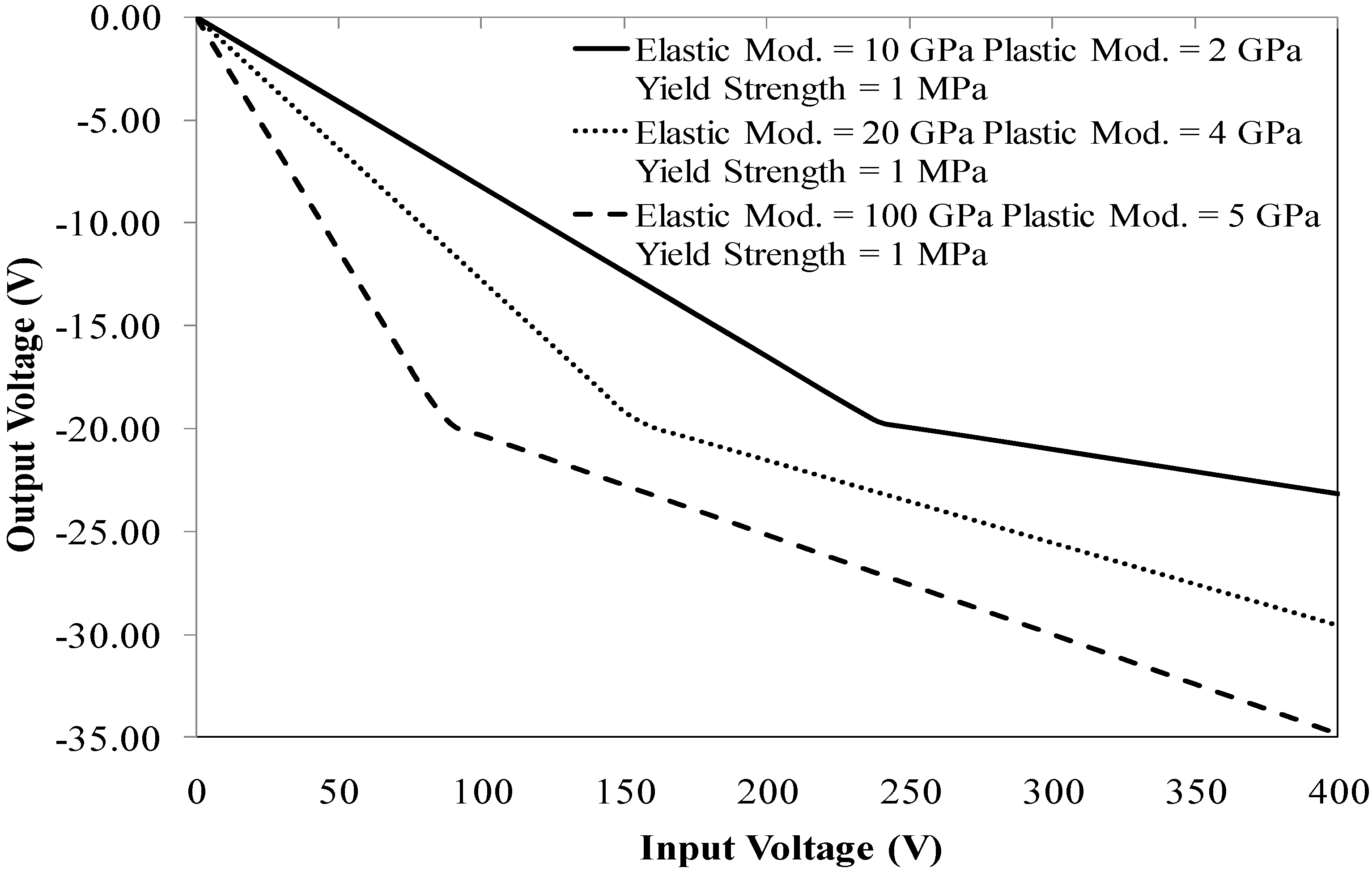
7.2. Plastic Characteristics
A similar analysis is conducted to generate a characteristic curve for elastic-plastic behavior as seen in
Figure 13 showing the response of the induced voltage for an array of material properties. The only difference being that both the elastic modulus and the plastic modulus (for the assumed bilinear hardening behavior) are varied. A low yield strength (1 MPa) is used for every case to keep the applied and induced voltages within a reasonable range.
Figure 13.
Induced voltage resulting from applied voltage for a range of test specimen properties.
Figure 13.
Induced voltage resulting from applied voltage for a range of test specimen properties.
Note again that the voltage response is linear in both the elastic and plastic regions. Therefore these plots are valid for materials that respond plastically in a bilinear manner, where the slopes of the output voltage in the elastic and plastic regimes are directly proportional to the elastic modulus and tangent modulus, respectively. It is reasonable to conclude that the response of the induced voltage above the yield point will mimic the plastic behavior of the test material, allowing for the appropriate hardening law to be derived from a curve fit of the induced voltage.
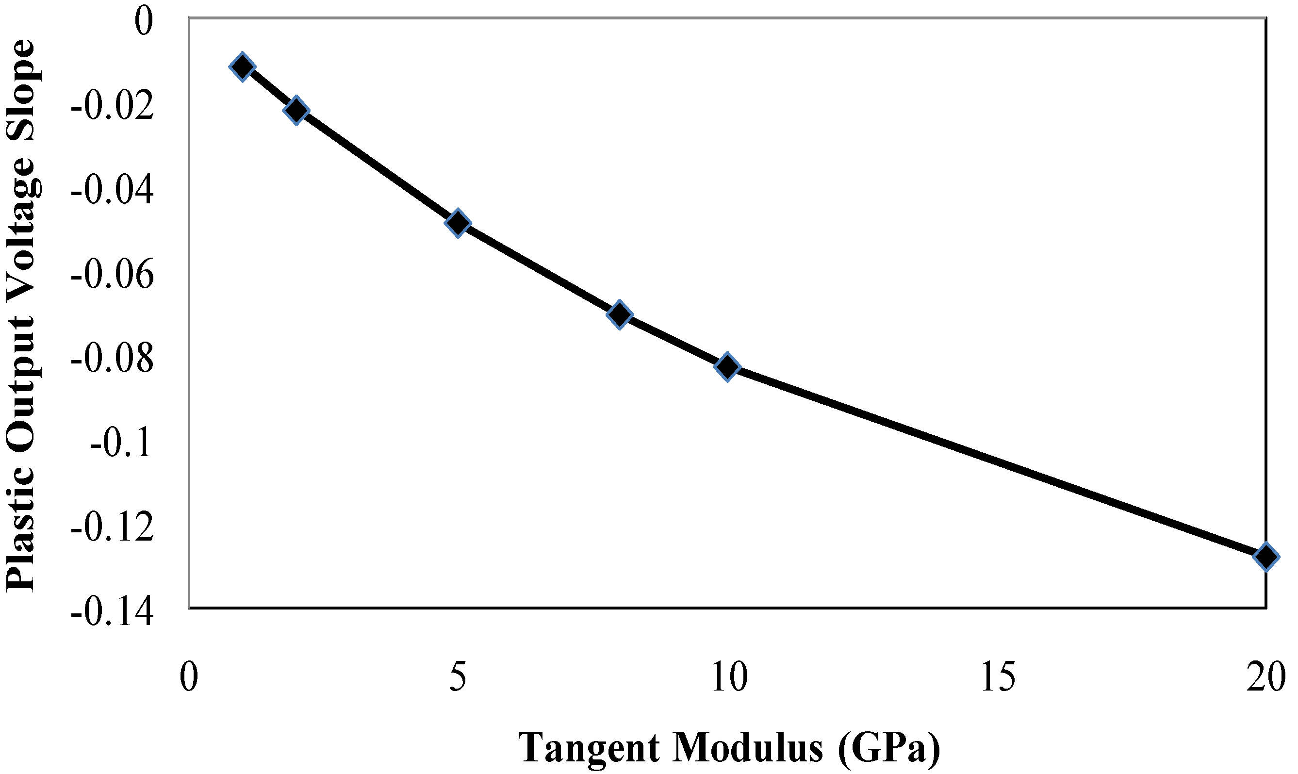
To further illustrate that the induced voltage response reproduces the bilinear plastic behavior,
Figure 14 shows how the slope of the output voltage changes with respect to a change in the plastic tangent modulus. The almost linear response of induced voltage slope relative to an increase in tangent modulus shows that the slope of the induced voltage is proportional to the tangent modulus. This indicates that when materials that exhibit more realistic hardening behavior are tested, the constants used for their curve fits will follow a similar trend.
Figure 14.
Comparison of the slope of the output voltage to the plastic tangent modulus.
Figure 14.
Comparison of the slope of the output voltage to the plastic tangent modulus.
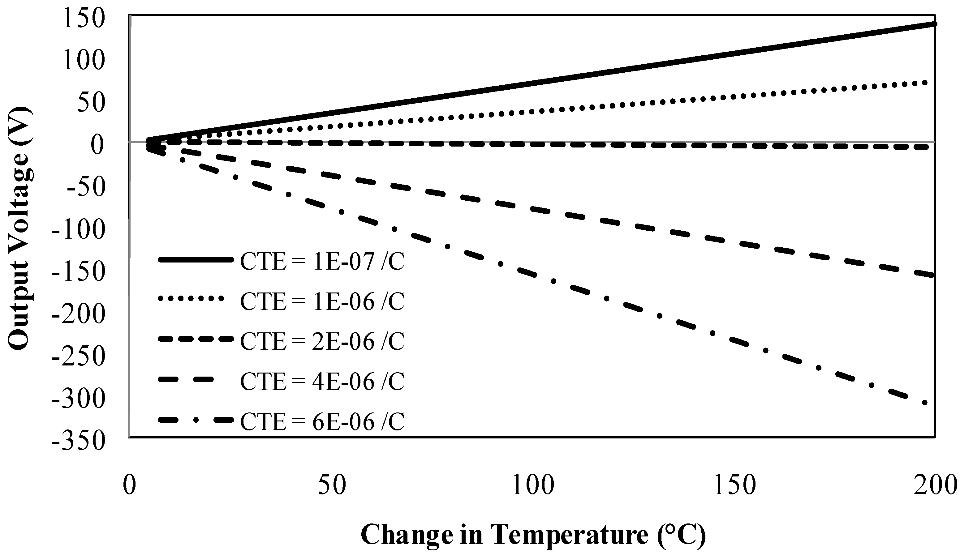
7.3. Thermal Characteristics
Finally, the induced voltage response for test materials with a range of CTEs is plotted relative to the change in temperature in
Figure 15. The elastic material properties shown in
Table 1 are used for every CTE value. Note that for low test material CTEs the output voltage is positive, indicating that the piezoelectric material exhibits tensile deformation, compressing the test material. Conversely, when the test material has a high CTE, the output voltage is negative, indicating that the piezoelectric material undergoes compressive deformation, resulting for the test material deforming in tension. There is a balance when the test material CTE is approximately 2E-06 °C
−1, and is governed by the relation shown in Equation 38.
Figure 15.
Induced voltage response relative to the change in temperature for a range of CTEs.
Figure 15.
Induced voltage response relative to the change in temperature for a range of CTEs.
When the products of CTE and Young’s modulus are equal for the piezoelectric material and the test material, the deformations throughout the sensor system will be completely balanced, and there will be no induced voltage. Similarly, when the inequality favors the test material, the output voltage will be negative. And when the inequality favors the piezoelectric material, the output voltage will be positive.
8. Device and Material Considerations
Although applicable to any scale, the proposed method is more feasible in meso and microscale. The electric field is inversely proportional to the piezoelectric member thickness. Therefore, achieving same electric field and same amount of strain at larger scale may require a large amount of voltage that can exceed the dielectric breakdown limit of the piezoelectric material. Therefore, this device is far more practical in small scales.
It should be noted that piezoelectric material are typically used when large amount of force is required. Therefore, piezoelectric members are suitable for testing stiffer material with estimated stiffness between 10 to 100 GPa. However, softer material such as some polymers and bio-material may have stiffness much smaller than this range. Depending on the type of test material and the amount of strain required in the system, other electro-active material such as, electro-active polymers, may be used, particularly for testing softer material such as tissues and cells. Electro-active polymers [
21,
22] can produce high levels of strain without inducing large amount of forces.
Compression tests can easily be conducted using this device as the forces generated in the system will hold the specimen in place. The analyses conducted in this manuscript are mostly at compression state. However, this device may also be used for tensile testing of material. In this case the test material must be attached to piezoelectric members. Therefore, another intermediate adhesive or coupling device must be used to attach the test material to piezoelectric members. Selecting a bonding agent that is strong enough to maintain full adhesion during loading is imperative. Determining the compliance of the interface medium for calibration and data processing purposes is also of utmost importance. Additionally, a negative voltage must be applied in such a way as to cause a compressive deformation in the first piezoelectric member and induce a positive (tensile) voltage in the second piezoelectric member.
It must also be noted that large amount of forces developed in the system may force the piezoelectric members to deform beyond elastic limits. Since piezoelectric materials are very brittle and stressing them beyond their elastic limit is undesirable. Furthermore, the level of complexity in deciphering the strain measured by a sensor that is itself plastically deforming is daunting. Therefore, it is suggested to start with small input voltages and increase the voltage incrementally with small increments to achieve the required force without exceeding the elastic limit of the piezoelectric members.
This should also be noted that the device is proposed to be used in quasi-static mode. Dynamic analysis using high frequency excitation of piezoelectric members can also be used to determine the material properties.
Difficulties are always present at the microscale. Fabricating properly shaped and dimensioned piezoelectric members and test samples may prove difficult. Also, attaching electrical leads large enough to produce and read the electric fields in the piezoelectric members will not be simple. Even affixing the strain sensing system within a rigid frame where the compliance is known and accounted for is difficult. Misalignments and microscopic imperfections at the interface of the three members produce significant deviations from the expected at this small a scale.
But all of these difficulties are present in any testing done at the micro-scale or lower and should not detract from the simplicity of the proposed device itself. Surrounding the test material with two piezoelectric members, all with the same thickness, allows strain measurements of the test sample be made using only the voltage applied to the first member and the voltage induced in the second member. The calibration and post-processing required is not any more involved or difficult than what is required in any other strain measurement device.
9. Conclusion and Summary
This piezoelectric strain sensing system shows a lot of promise in its applicability as an accurate strain measurement device in micro-scale environments. Though there are a number of calculations that must be made to use the sensor, they are by no means complex. All that is required are some simple constitutive equations that relate the electromechanical deformation in the piezoelectric members to the mechanical deformation in the test segment.
The original concept of the device using equivalently sized piezoelectric and test segments is shown to have analytical and FE solutions that agree very well. Any discrepancies are completely proportional, and with proper calibration and proportionality factors, the analytical equations can be easily modified to agree with the FE results.
For inelastic deformation, modifications to the equivalent segment device are required to produce accurate results. By making the piezoelectric segments larger than the test segment, the inelastic behavior of the test material predicted both analytically and using a FE model. Of course, there is a large degree of variability between the two solutions below the yield strength of the test material. But since the elastic solution is more easily obtained using the equivalent segment configuration, only the purely plastic results are compared, and they agree very well.
Another modification that shows promise is using notched segments. This serves to decrease the variance between the analytical and FE solutions, but the results in both the elastic and inelastic regimes still deviate more than is acceptable. One may be able to further modify the notched configuration by increasing the size, aspect ratio, or placement of the notch, but that is not investigated here.
Despite there being some logistical kinks to work out, the piezoelectric device investigated here shows a lot of promise as a small scale measurement device. It can be used to measure deformation in both the elastic and inelastic regions of deformation, as well as deformation due to thermal loading. Analytically, the relationships for all three types of loading are not overly complicated, and the modifications required to change from one test to the next are minimal.
The suitability to a certain application depends of the type of electroactive material. For stiffer material the electroactive material need to insert large amount of force and therefore, piezoelectric material (which typically are ceramic material with large stiffness) are more suitable for stiffer material. However, large forces may also introduce more deformation in the rigid frame and increase the amount of error. Furthermore, finding a material for rigid frame with higher stiffness than piezoelectric material may not be always possible. However, when testing softer materials the forces generated in the system are not large and do not introduce large deformation in the rigid frame. Additionally, finding a rigid frame that is stiffer than polymer electroactive members is much more likely. Therefore, the amount of error is much smaller and in general this device is more accurate in softer materials. Since the linear behavior can be predicted almost accurately, this device is recommended for use for stresses applied under specimen’s yield stress. Further modification may make the device more accurate in testing material with inelastic behavior. If a material with non-linear plastic behavior is used, similar methodology may be utilized to characterize the material behavior.


