A Flexible Capacitive Sensor with Encapsulated Liquids as Dielectrics


Abstract
:1. Introduction

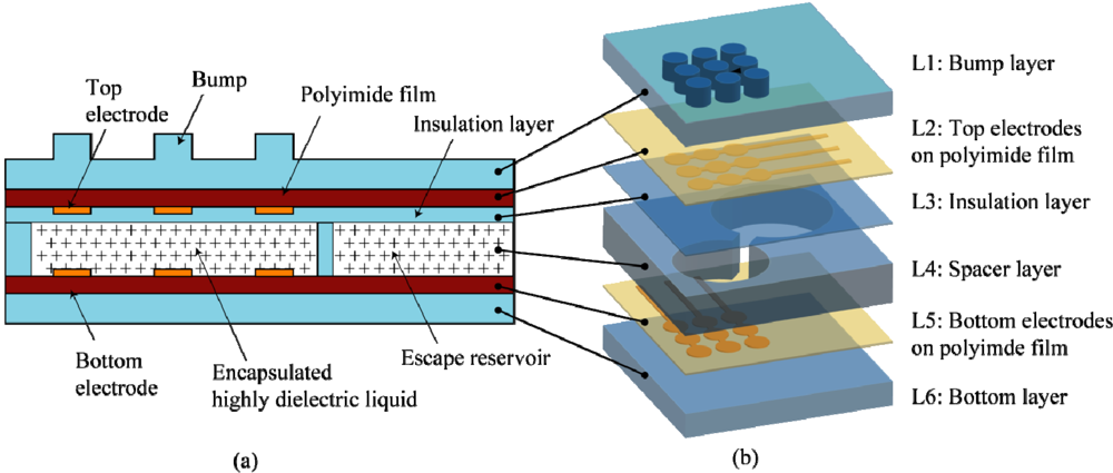
2. Design

3. Experimental Section
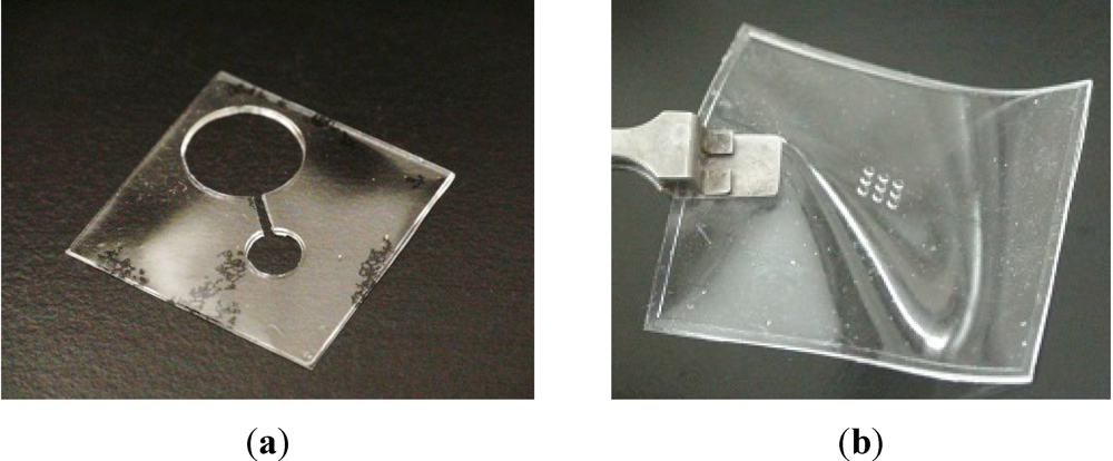
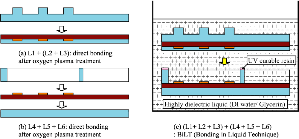
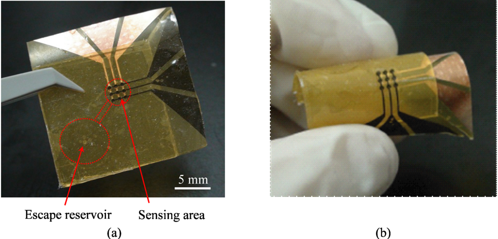
3.1. Fabrication


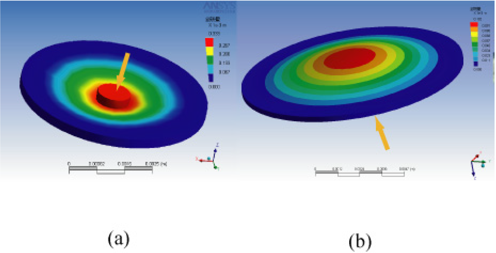
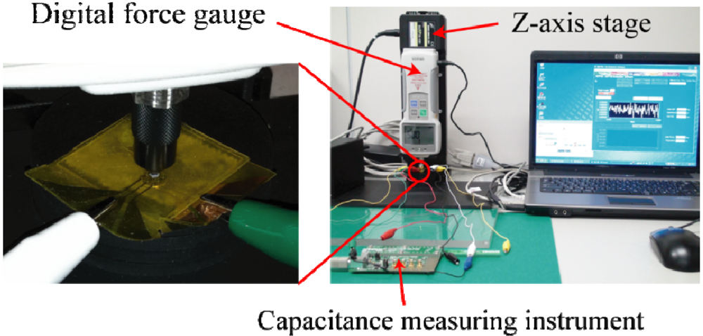
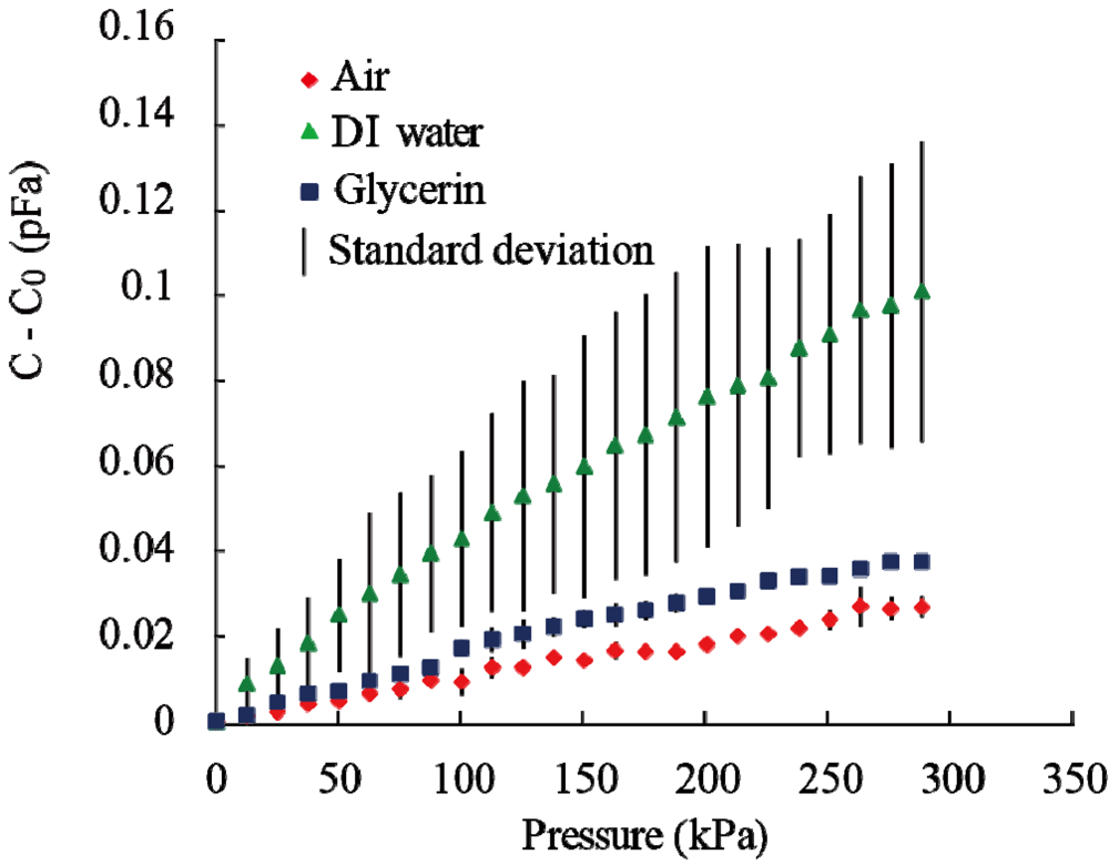
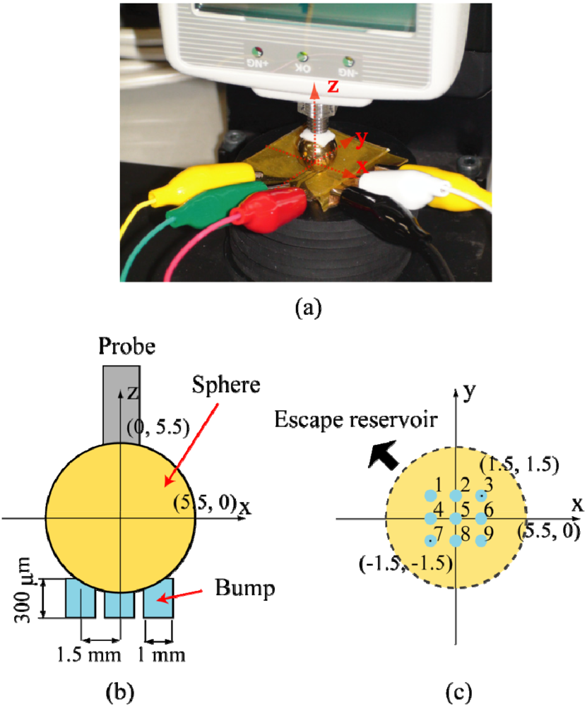
3.2. Experimental Results


4. Conclusions
Acknowledgments
References
- Eltaib, M.E.H.; Hewit, J.R. Tactile sensing technology for minimal access surgery—A review. Mechatronics 2003, 13, 1163–1177. [Google Scholar]
- Zhu, F.; Spronck, J.W. A capacitive tactile sensor for shear and normal force measurements. Sens. Actuat. A 1992, 31, 115–120. [Google Scholar]
- Hoshi, T.; Shinoda, H. Robot Skin based on Touch-Area-Sensitive Tactile Element. In Proceedings of the 2006 IEEE International Conference on Robotics and Automation, Orlando, FL, USA, 15–19 May 2006; pp. 3463–3468.
- Cheng, M.-Y.; Lin, C.-L.; Yang, Y.-J. Tactile and Shear Stress Sensing Array Using Capacitive Mechanisms with Floating Electrodes. In Proceedings of 2010 IEEE 23rd International Conference on Micro Electro Mechanical Systems (MEMS), Wanchai, Hong Kong, 24–28 January 2010; pp. 228–231.
- Lee, H.K.; Chung, J.; Chang, S.-I.; Yoon, E. Normal and shear force measurement using a flexible polymer tactile sensor with embedded multiple capacitors. J. Microelectromech. Syst. 2008, 17, 934–942. [Google Scholar] [CrossRef]
- Lee, H.K.; Chang, S.-I.; Yoon, E. A flexible polymer tactile sensor: Fabrication and modular expandability for large area deployment. J. Microelectromech. Syst. 2006, 15, 1681–1686. [Google Scholar] [CrossRef]
- Shimojo, M.; Namiki, A.; Ishikawa, M.; Makino, R.; Mabuchi, K. A tactile sensor sheet using pressure conductive rubber with electrical-wires stitched method. IEEE Sens. J. 2004, 4, 589–596. [Google Scholar]
- Castellanos-Ramos, J.; Navas-González, R.; Macicior, H.; Sikora, T.; Ochoteco, E.; Vidal-Verdú, F. Tactile sensors based on conductive polymers. Microsyst. Technol. 2010, 16, 765–776. [Google Scholar]
- Begej, S. Planar and finger-shaped optical tactile sensors for robotic applications. IEEE J. Robot. Autom. 1988, 4, 472–484. [Google Scholar]
- Watanabe, N.; Moriyama, N. Grip force control using vision-based tactile sensor for dexterous handling. Eur. Robot. Symp. 2008, 44, 113–122. [Google Scholar]
- Zhang, Y.; Miki, N. Sensitivity enhancement of a micro-scale biomimetic tactile sensor with epidermal ridges. J. Micromech. Microeng. 2010, 20. [Google Scholar] [CrossRef]
- Lee, M.H.; Nicholls, H.R. Review article tactile sensing for mechatronics—A state of the art survey. Mechatronics 1999, 9, 1–31. [Google Scholar]
- Dahiya, R.S.; Metta, G.; Valle, M.; Sandini, G. Tactile sensing—From humans to humanoids. Robotics 2010, 26, 1–20. [Google Scholar]
- De Souza, R.J.; Wise, K.D. A Very High Density Bulk Micromachined Capacitive Tactile Imager. In Proceedings of the International Conference on Solid State Sensors and Actuators (TRANSDUCERS ’97), Chicago, IL, USA, 16–19 June 1997; pp. 1473–1476.
- Peng, P.; Rajamani, R.; Erdman, A.G. Flexible tactile sensor for tissue elasticity measurements. J. Microelectromech. Syst. 2009, 18, 1226–1233. [Google Scholar]
- Kim, H.-K.; Lee, S.-G.; Han, J.-E.; Kim, T.-R.; Hwang, S.-U.; Ahn, S.D.; You, I.-K.; Cho, K.-I.; Song, T.-K.; Yun, K.-S. Transparent and Flexible Tactile Sensor for Multi Touch Screen Application with Force Sensing. In Proceedings of the International Actuators and Microsystems Conference on Solid-State Sensors, (TRANSDUCERS 2009), Denver, CO, USA, 21–25 June 2009; pp. 1146–1149.
- Ko, C.-T.; Wu, J.-P.; Wang, W.-C.; Huang, C.-H.; Tseng, S.-H.; Chen, Y.-L.; Lu, M.S.-C. A Highly Sensitive CMOS-MEMS Capacitive Tactile Sensor. In Proceedings of the 2006 IEEE 19th International Conference on Micro Electro Mechanical Systems (MEMS), Istanbul, Turkey, 22–26 January 2006; pp. 642–645.
- Wibbeler, J.; Pfeifer, G.; Hietschold, M. Parasitic charging of dielectric surfaces in capacitive microelectromechanical systems (MEMS). Sens. Actuat. A 1998, 71, 74–80. [Google Scholar]
- Fujimori, T.; Hanaoka, Y.; Fukuda, H. Above-IC Integration of Capacitive Pressure Sensor Fabricated with CMOS Interconnect Processes. In Proceedings of the 2007 IEEE 19th International Conference on Micro Electro Mechanical Systems (MEMS), Hyogo, Japan, 21-25 January 2007; pp. 43–46.
- Salo, T.; Kirstein, K.-U.; Sedivy, J.; Grunenfelder, J.; Vancura, T.;Zund, G; Baltes, H. Continuous blood pressure monitoring utilizing a CMOS tactile sensor. Eng. Med. Biol. Soc. 2004, 3, 23226–23229. [Google Scholar]
- Hezarjaribi, Y.; Hamidon, M.N.; Keshmiri, S.H.; Bahadorimehr, A.R. Capacitive Pressure Sensors based on MEMS, Operating in Harsh Environments. In Proceedings of the 2008 IEEE International Conference on Semiconductor Electronics, Johor Bahru, Malaysia, 25-27 November 2008; pp. 184–187.
- Wang, S.; Feng, Y. Micro Capacitive Vacuum Sensor Based on MEMS. In Proceedings of the 5th IEEE International Conference on Nano/Micro Engineered and Molecular Systems (NEMS), Xiamen, China, 20–23 January 2010; pp. 1160–1164.
- Cheng, M.-Y.; Tsao, C.-M.; Lai, Y.-T.; Yang, Y.-J. A Novel Highly-Twistable Tactile Sensing Array Using Extendable Spiral Electrodes. In Proceedings of the 2009 IEEE 21th International Conference on Micro Electro Mechanical Systems (MEMS), Sorrento, Italy, 25–29 January 2009; pp. 92–95.
- Noda, K.; Hoshino, K.; Matsumoto, K.; Shimoyama, I. A shear stress sensor for tactile sensing with the piezoresistive cantilever standing in elastic material. Sens. Actuat. A 2006, 127, 295–301. [Google Scholar]
- Shimojo, M.; Namiki, A.; Ishikawa, M.; Makino, R.; Mabuchi, K. A tactile sensor sheet using pressure conductive rubber with electrical-wires stitched method. IEEE Sens. J. 2004, 4, 589–596. [Google Scholar]
- Kerpa, O.; Weiss, K.; Worn, H. Development of a Flexible Tactile Sensor System for a Humanoid Robot. In Proceedings of the 2003 IEEE/RSJ International Conference on Intelligent Robots and Systems, Nice, France, 22–26 September 2003; pp. 1–6.
- Engel, J.; Chen, J.; Liu, C. Development of polyimide flexible tactile sensor skin. J. Micromech. Microeng. 2003, 13, 359–366. [Google Scholar]
- Huan, X.-D.; Huan, J.-Q.; Qin, M.; Huan, Q.-A. A Fully Integrated Capacitive Pressure Sensor with High Sensitivity. In Proceedings of the IEEE Sensors 2007 Conference, Atlanta, GA, USA, 28–31 October 2007; pp. 1052–1055.
- Shkel, Y.M.; Ferrier, N.J. Electrostriction enhancement of solid-state capacitance sensing. Mechatronics 2003, 8, 318–325. [Google Scholar]
- Thakur, O.P.; Singh, A.K. Modeling of Capacitive Sensor Filled with Elastic Dielectrics and Its Advantages. In Proceedings of the 3rd International Conference on Sensing Technology, Tainan, Taiwan, 30 November–3 December 2008; pp. 467–471.
- Khiem, N.B.; Matsumoto, K.; Shimoyama, I. Polymer thin film deposited on liquid for varifocal encapsulated liquid lenses. Appl. Phys. Lett. 2008, 93. [Google Scholar] [CrossRef]
- Kim, H.; Najafi, K. An Electrically-Driven, Large-Deflection, High-Force, Micro Piston Hydraulic Actuator Array for Large-Scale Microfluidic Systems. In Proceedings of the 2009 IEEE 21th International Conference on Micro Electro Mechanical Systems (MEMS), Sorrento, Italy, 25–29 January 2009; pp. 483–486.
- Arouette, X.; Matsumoto, Y.; Ninomiya, T.; Okayama, Y.; Miki, N. Dynamic characteristics of a hydraulic amplification mechanism for large displacement actuators systems. Sensors 2010, 10, 2946–2956. [Google Scholar]
- Ninomiya, T.; Okayama, Y.; Matsumoto, Y.; Arouette, X.; Osawa, K.; Miki, N. MEMS-based hydraulic displacement amplification mechanism with completely encapsulated liquid. Sens. Actuat. A 2011, 166, 277–282. [Google Scholar]
- Okayama, Y.; Nakahara, K.; Arouette, X.; Ninomiya, T.; Matsumoto, Y.; Orimo, Y.; Hotta, A.; Omiya, M.; Miki, N. Characterization of a bonding-in-liquid technique for liquid encapsulation into MEMS devices. J. Micromech. Microeng. 2010, 20. [Google Scholar] [CrossRef]
- Antelius, M.; Fischer, A.C.; Niklaus, F.; Stemme, G.; Roxhed, N. Hermetic Integration of Liquids in MEMS by Room Temperature, High-Speed Plugging of Liquid-Filled Cavities at Wafer Level. In Proceedings of the 2011 IEEE 24th International Conference on Micro Electro Mechanical Systems (MEMS), Cancun, Mexico, 23–27 January 2011; pp. 356–359.
- Hotta, Y.; Zhang, Y.; Miki, N. Flexible Distributed Capacitive Sensor with Encapsulated Ferroelectric Liquid. In Proceedings of the 2011 IEEE 24th International Conference on Micro Electro Mechanical Systems (MEMS), Cancun, Mexico, 23–27 January 2011; pp. 573–576.
- Fuard, D.; Tzvetkova-Chevolleau, T.; Decossas, S.; Tracqui, P.; Schiavone, P. Optimization of poly-di-methyl-siloxane (PDMS) substrates for studying cellular adhesion and motility. Microelectron. Eng. 2008, 85, 1289–1293. [Google Scholar]
- Miki, N.; Teo, C.J.; Ho, L.C.; Zhang, X. Enhancement of rotordynamic performance of high-speed micro-rotors for power MEMS applications by precision deep reactive ion etching. Sens. Actuat. A 2003, 104, 263–267. [Google Scholar]
- Miki, N. Wafer bonding techniques for MEMS. Sens. Lett. 2005, 3, 263–273. [Google Scholar]
- Sawano, S.; Naka, K.; Werber, A.; Zappe, H.; Konishi, S. Sealing Method of PDMS as Elastic Material for MEMS. In Proceedings of the 2008 IEEE 21st International Conference on Micro Electro Mechanical Systems (MEMS), Tucson, AZ, USA, 13–17 January 2008; pp. 419–422.
© 2012 by the authors; licensee MDPI, Basel, Switzerland. This article is an open-access article distributed under the terms and conditions of the Creative Commons Attribution license (http://creativecommons.org/licenses/by/3.0/).
Share and Cite
Hotta, Y.; Zhang, Y.; Miki, N. A Flexible Capacitive Sensor with Encapsulated Liquids as Dielectrics. Micromachines 2012, 3, 137-149. https://doi.org/10.3390/mi3010137
Hotta Y, Zhang Y, Miki N. A Flexible Capacitive Sensor with Encapsulated Liquids as Dielectrics. Micromachines. 2012; 3(1):137-149. https://doi.org/10.3390/mi3010137
Chicago/Turabian StyleHotta, Yasunari, Yuhua Zhang, and Norihisa Miki. 2012. "A Flexible Capacitive Sensor with Encapsulated Liquids as Dielectrics" Micromachines 3, no. 1: 137-149. https://doi.org/10.3390/mi3010137