Design of an Angle Detector for Laser Beams Based on Grating Coupling

Abstract
:
1. Introduction
2. Design of the Angle Detector Based on Grating Coupling
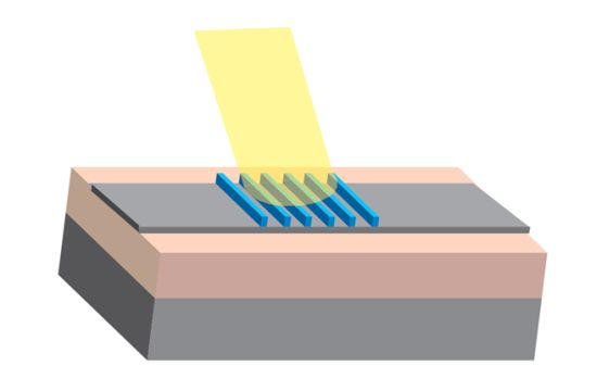
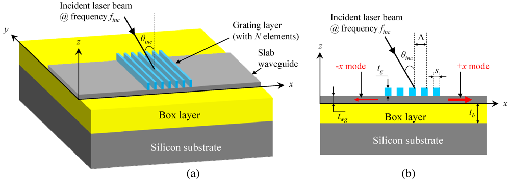
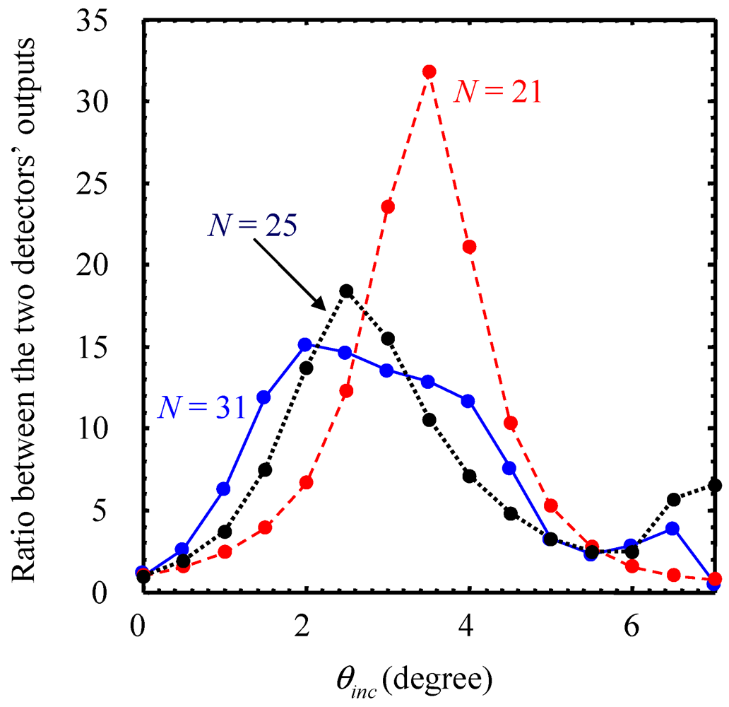
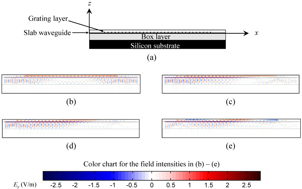
 . The grating layer sits on top of an SOI slab waveguide. A laser beam with frequency finc is incident onto the device from the top. The incident direction is in the x–z plane. The angle between the incident laser and z direction (i.e., surface normal direction) is denoted as θinc. When the laser is incident obliquely, θinc takes positive values when the incident laser is along +x direction and θincis negative when the incident laser is along –x direction. Our device is designed such that the incident light is efficiently coupled to the “+x traveling mode” and “−x traveling mode” in the slab waveguide. When θinc = 0 (that is, normal incidence), “+x mode” and “−x mode” in the slab waveguide are equally strong, due to the geometrical symmetry. When θinc ≠ 0 (that is, oblique incidence), the “+x mode” and “−x mode” are unbalanced. As a result, θinc can be found by comparing the “+x mode” and “−x mode.” In our device, the “+x mode” and “−x mode” are observed by placing two detectors in the slab waveguide. The two detectors are named “+x detector” and “−x detector,” respectively. The “+x detector” is placed to the right of the grating structure and it serves to detect the power of the “+x mode;” similarly, the “−x detector” is placed to the left of the grating structure and it detects the power of the “−x mode.” The photodetectors in the waveguide can be implemented by following available architectures in [16,17,18].
 (1)
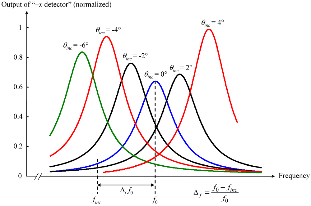
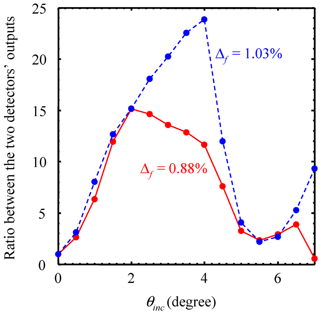
(1) is the wavenumber along x for the fundamental guided mode in the slab waveguide. It is noted that is non-linear with respect to the frequency. The transverse resonant frequency for θinc = 0 is denoted as “f0.” The transverse resonant frequency increases with the increase of θinc, as shown in Figure 2. Bandwidth of the resonance is measured by finding the frequencies at which the photodetector’s output drops by 3 dB with respect to the value at the resonant frequency. Further, quality factor is defined as the ratio between the resonant frequency and the bandwidth.
 (2)
(2)
3. Numerical Results


4. Conclusions
Acknowledgments
References and Notes
- Mawatari, K.; Shimoide, K. Reflective thermal lens detection device. Lab Chip 2006, 6, 127–130. [Google Scholar] [CrossRef]
- Müller, H.; Chiow, S.-W.; Long, Q.; Vo, C.; Chu, S. Active sub-Rayleigh alignment of parallel or antiparallel laser beams. Opt. Lett. 2005, 30, 3323–3325. [Google Scholar] [CrossRef]
- Mukai, S.; Watanabe, M.; Itoh, H.; Yajima, H.; Hosoi, Y.; Uekusa, S. Beam scanning and switching characteristics of twin-striped lasers with a reduced stripe spacing. Opt. Quant. Electron. 1985, 17, 431–434. [Google Scholar] [CrossRef]
- Scifres, D.R.; Streifer, W.; Burnham, R.D. Beam scanning with twin-stripe injection-lasers. Appl. Phys. Lett. 1978, 33, 702–704. [Google Scholar]
- Kurosaka, Y.; Iwahashi, S.; Liang, Y.; Sakai, K.; Miyai, E.; Kunishi, W.; Ohnishi, D.; Noda, S. On-chip beam-steering photonic-crystal lasers. Nat. Photon. 2010, 4, 447–450. [Google Scholar] [CrossRef]
- Tuantranont, A.; Bright, V.M.; Zhang, J.; Zhang, W.; Neff, J.A.; Lee, Y.C. Optical beam steering using MEMS-controllable microlens array. Sensors Actuat. A: Phys. 2001, 91, 363–372. [Google Scholar] [CrossRef]
- May-Arrioja, D.A.; Bickel, N.; LiKamWa, P. Optical beam steering using InGaAsP multiple quantum wells. IEEE Photonic Technol. Lett. 2005, 17, 333–335. [Google Scholar]
- Jarrahi, M.; Fabian, R.; Pease, W.; Miller, D.A.B.; Lee, T.H. High-speed optical beam-steering based on phase-arrayed waveguides. J. Vac. Sci. Technol. B 2008, 26, 2124–2126. [Google Scholar] [CrossRef]
- Nakamura, O.; Goto, M.; Toyoda, K.; Takai, N.; Kurosawa, T.; Nakamata, T. A laser tracking robot-performance calibration system using ball-seated bearing mechanisms and a spherically shaped cat’s-eye retroreflector. Rev. Sci. Instr. 1994, 65, 1006. [Google Scholar] [CrossRef]
- Umetsu, K.; Furutnani, R.; Osawa, S.; Takatsuji, T.; Kurosawa, T. Geometric calibration of a coordinate measuring machine using a laser tracking system. Meas. Sci. Technol. 2005, 16, 2466–2472. [Google Scholar] [CrossRef]
- Manojlovic, L.M.; Barbaric, Z.P. Optimization of optical receiver parameters for pulsed laser-tracking systems. IEEE Trans. Instrum. Meas. 2009, 58, 681–690. [Google Scholar] [CrossRef]
- Toyoda, M.; Araki, K.; Suzuki, Y. Measurement of the characteristics of a quadrant avalanche photodiode and its application to a laser tracking system. Opt. Eng. 2002, 41, 145–149. [Google Scholar] [CrossRef]
- Makynen, A.; Kostamovaara, J.T.; Myllyla, R.A. Displacement sensing resolution of position-sensitive detectors in atmospheric turbulence using retroreflected beam. IEEE Trans. Instrum. Meas. 1997, 46, 1133–1136. [Google Scholar] [CrossRef]
- Fujita, T.; Nakamura, K.; Matozaki, T. Simple and accurate propagation-angle observation of a collimated laser beam within a short optical path range by use of a dual-focus Fresnel lens. Opt. Rev. 2005, 12, 260–263. [Google Scholar] [CrossRef]
- Kunz, R.E.; Dubendorfer, J. Novel miniature integrated optical goniometers. Sensor Actuat. A: Phys. 1997, 60, 23–28. [Google Scholar] [CrossRef]
- Roelkens, G.; Van Thourhout, D.; Baets, R.; Notzel, R.; Smit, M. Laser emission and photodetection in an InP/InGaAsP layer integrated on and coupled to a Silicon-on-Insulator waveguide circuit. Opt. Express 2006, 14, 8154–8159. [Google Scholar] [CrossRef]
- Liang, D.; Fiorentino, M.; Okumura, T.; Chang, H.-H.; Spencer, D.T.; Kuo, Y.-H.; Fang, A.W.; Dai, D.; Beausoleil, R. G.; Bowers, J. E. Electrically-pumped compact hybrid silicon microring lasers for optical interconnects. Opt. Express 2009, 17, 20355–20364. [Google Scholar]
- Roelkens, G.; Brouckaert, J.; Taillaert, D.; Dumon, P.; Bogaerts, W.; Van Thourhout, D.; Baets, R.; Notzel, R.; Smit, M. Integration of InP/InGaAsP photodetectors onto silicon-on-insulator waveguide circuits. Opt. Express 2005, 13, 10102–10108. [Google Scholar]
- Meep. Available online: http://ab-initio.mit.edu/wiki/index.php/Meep (accessed on 30 January 2012).
- Yang, X.; Yu, M.; Kwong, D.-L.; Wong, C.W. Coupled resonances in multiple silicon photonic crystal cavities in all-optical solid-state analogy to electromagnetically induced transparency. IEEE J. Sel. Top. Quantum Electr. 2010, 16, 288–294. [Google Scholar] [CrossRef]
- Baumann, K.; Stoferle, T.; Moll, N.; Raino, G.; Mahrt, R.F.; Wahlbrink, T.; Bolten, J.; Scherf, U. Design and optical characterization of photonic crystal lasers with organic gain material. J. Opt. 2010, 12, 065003. [Google Scholar] [CrossRef]
- Kim, T.-T.; Lee, S.-G.; Kim, S.-H.; Kim, J.-E.; Park, H. Y.; Kee, C.-S. Ring-type Fabry-Perot filter based on the self-collimation effect in a 2D photonic crystal. Opt. Express 2010, 18, 17106–17113. [Google Scholar]
© 2012 by the authors; licensee MDPI, Basel, Switzerland. This article is an open-access article distributed under the terms and conditions of the Creative Commons Attribution license (http://creativecommons.org/licenses/by/3.0/).
Share and Cite
Saha, T.K.; Lu, M.; Ma, Z.; Zhou, W. Design of an Angle Detector for Laser Beams Based on Grating Coupling. Micromachines 2012, 3, 36-44. https://doi.org/10.3390/mi3010036
Saha TK, Lu M, Ma Z, Zhou W. Design of an Angle Detector for Laser Beams Based on Grating Coupling. Micromachines. 2012; 3(1):36-44. https://doi.org/10.3390/mi3010036
Chicago/Turabian StyleSaha, Tapas Kumar, Mingyu Lu, Zhenqiang Ma, and Weidong Zhou. 2012. "Design of an Angle Detector for Laser Beams Based on Grating Coupling" Micromachines 3, no. 1: 36-44. https://doi.org/10.3390/mi3010036