Rapid Laser Manufacturing of Microfluidic Devices from Glass Substrates

 , , ,
, , ,  ,
,
Abstract
:1. Introduction
2. Materials and Methods
2.1. Material Used
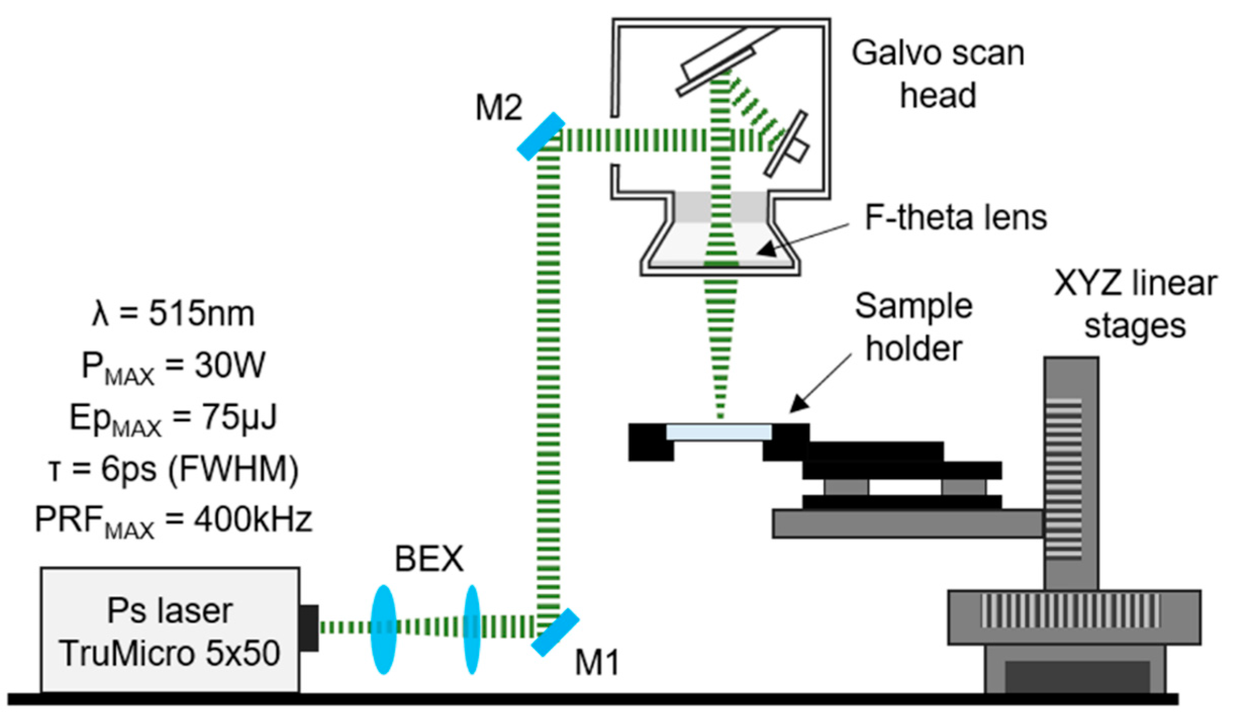
2.2. Laser System
2.3. Laser Micromachining Procedure
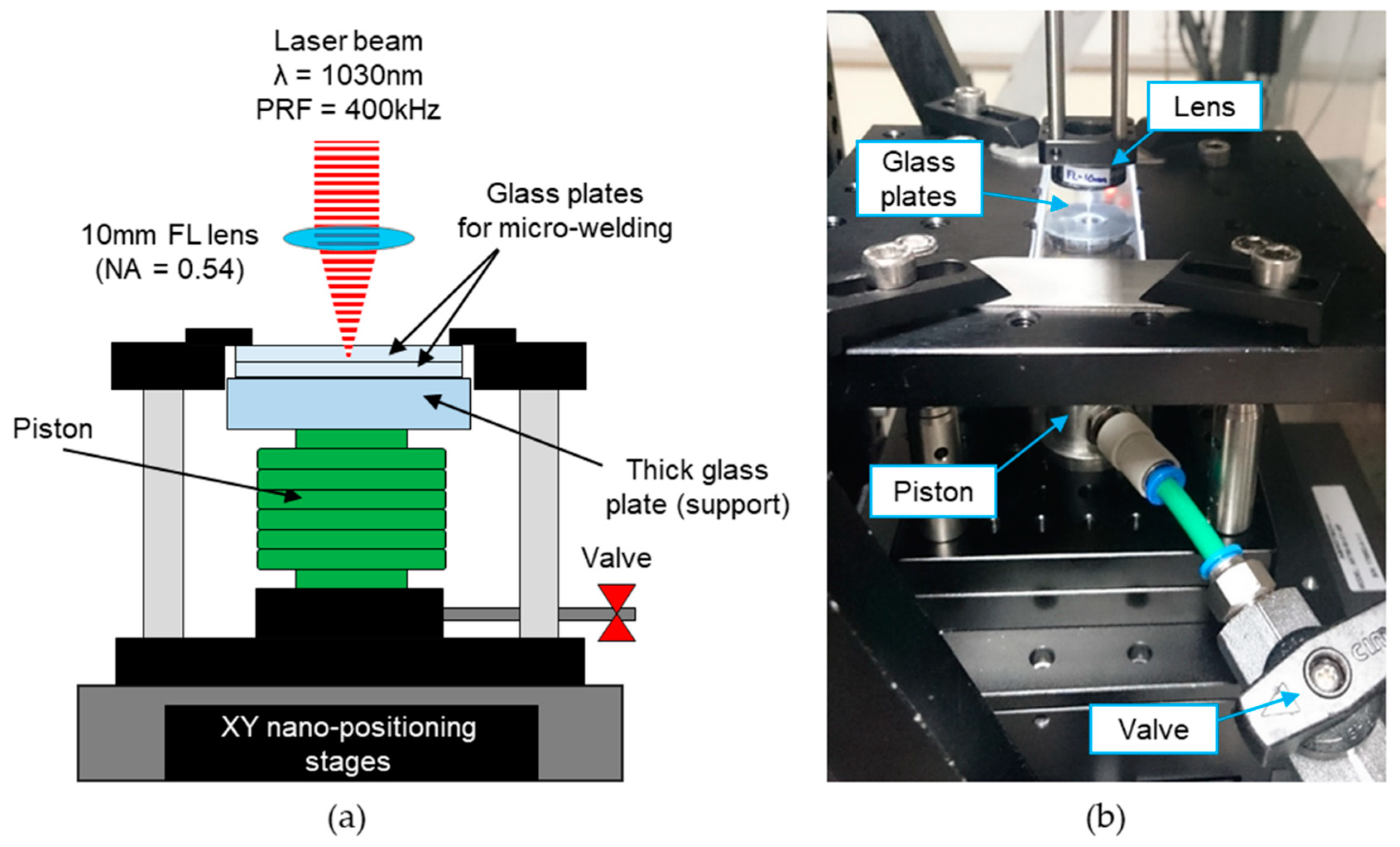
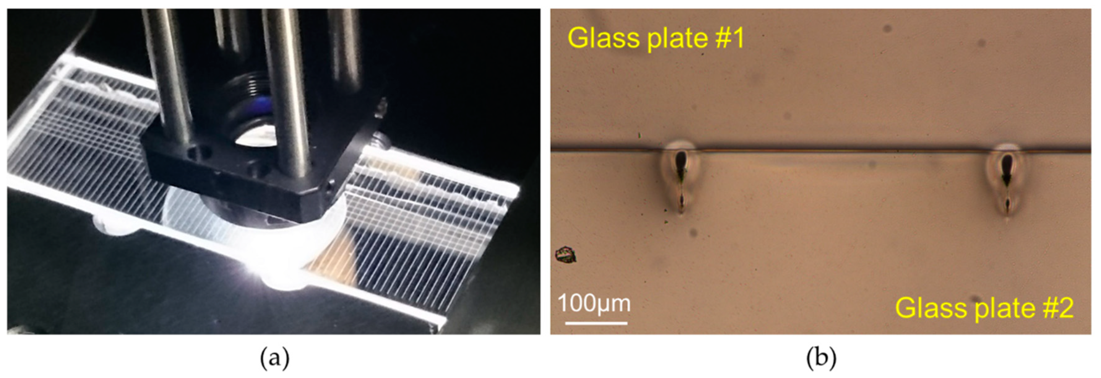
2.4. Laser Microwelding Procedure
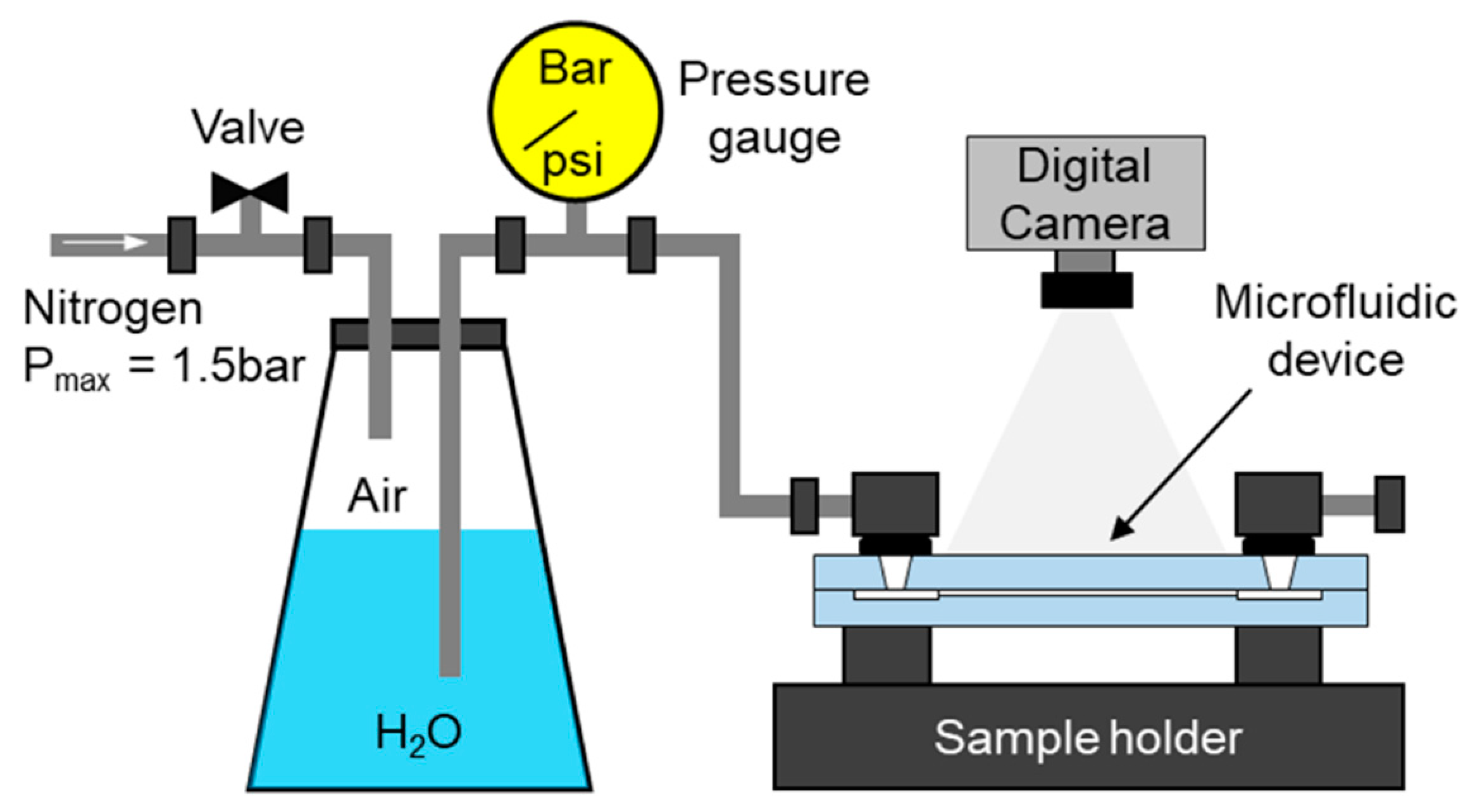
2.5. Testing of the Laser-Manufactured Microfluidic Devices
3. Results and Discussion
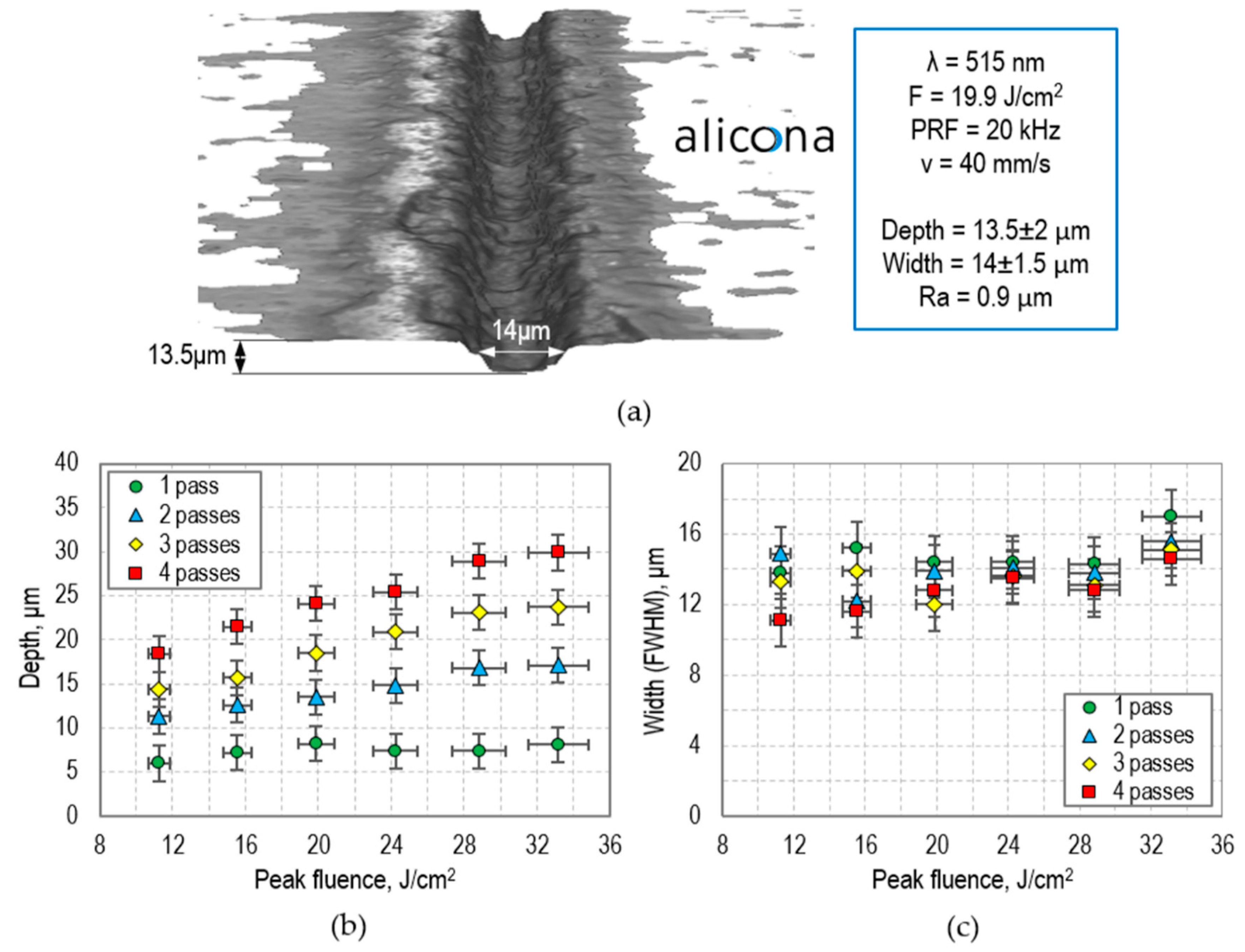
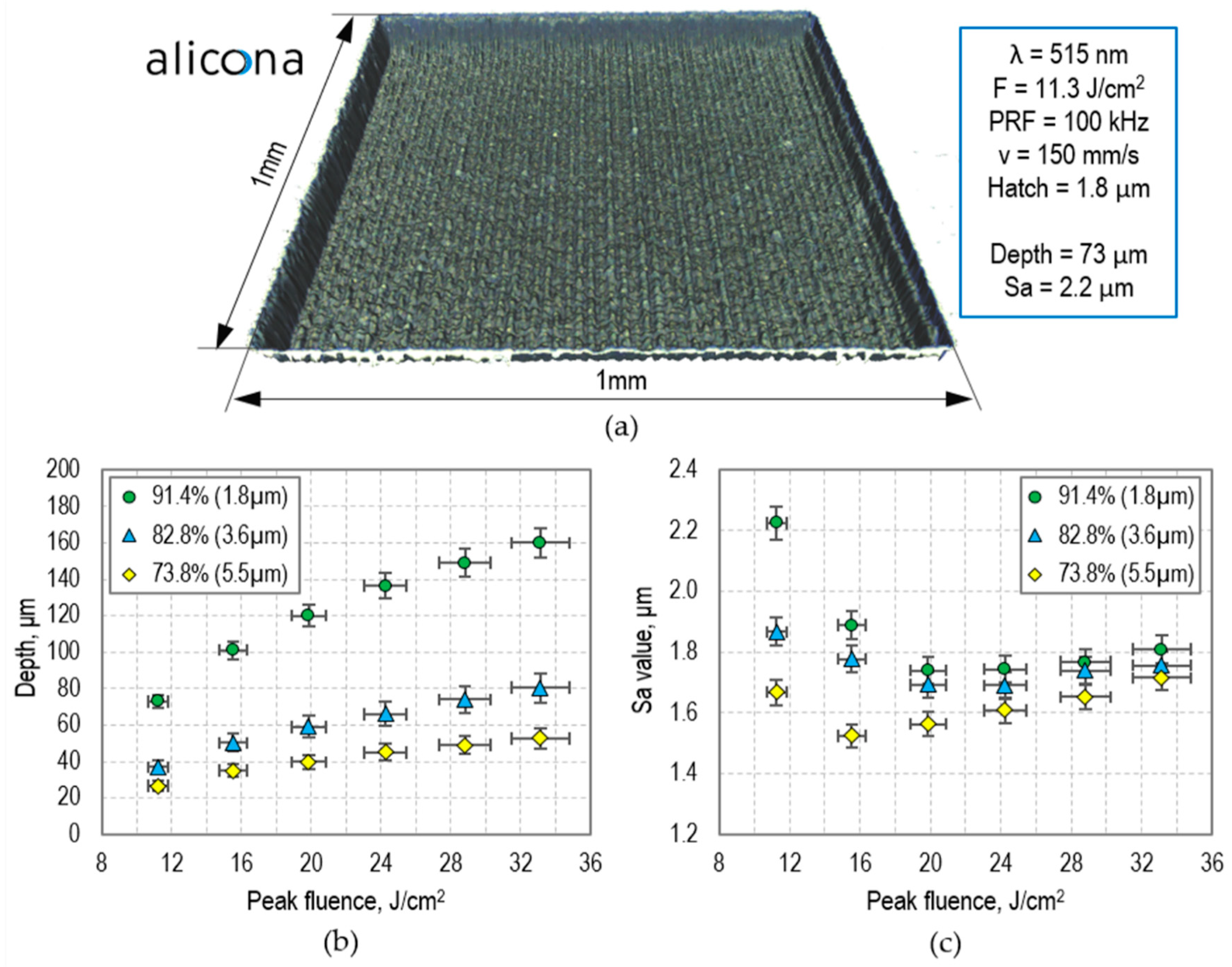
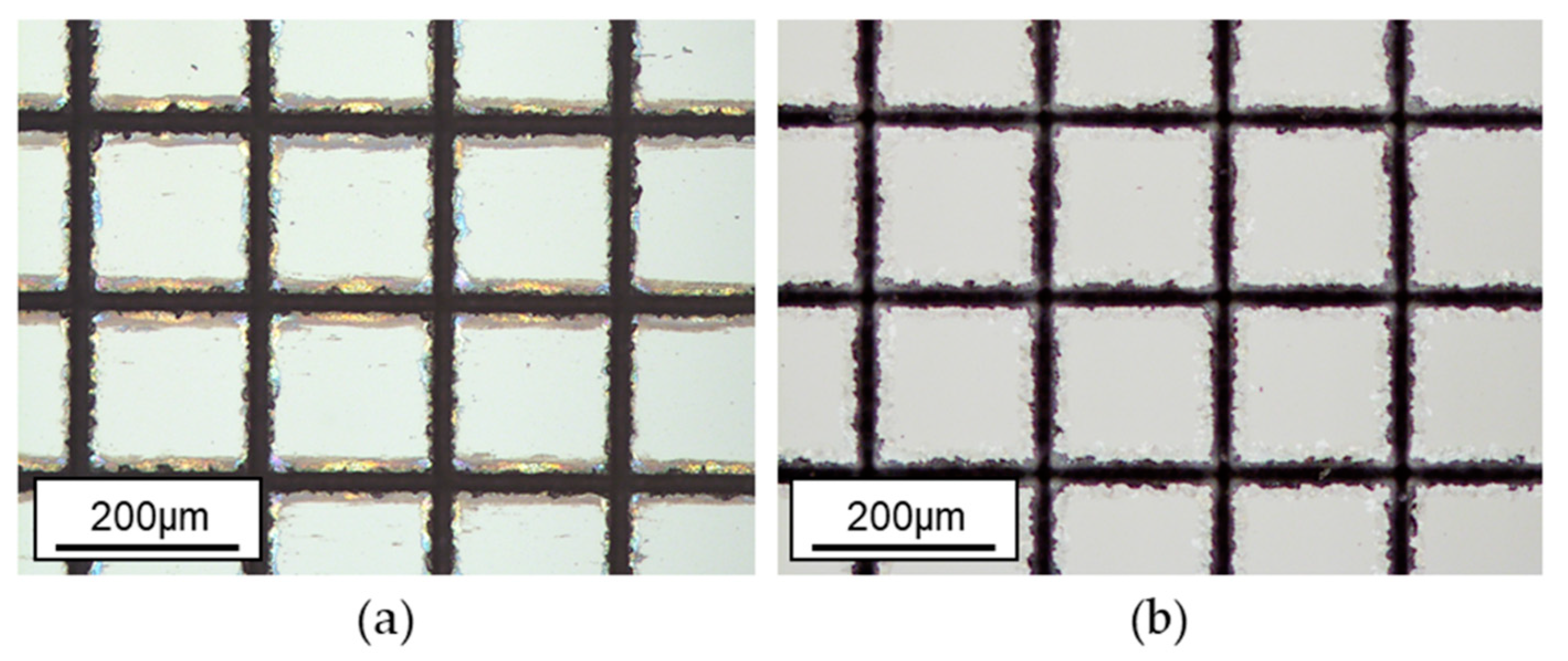
3.1. Calibration of the Laser Micro-Machining Process
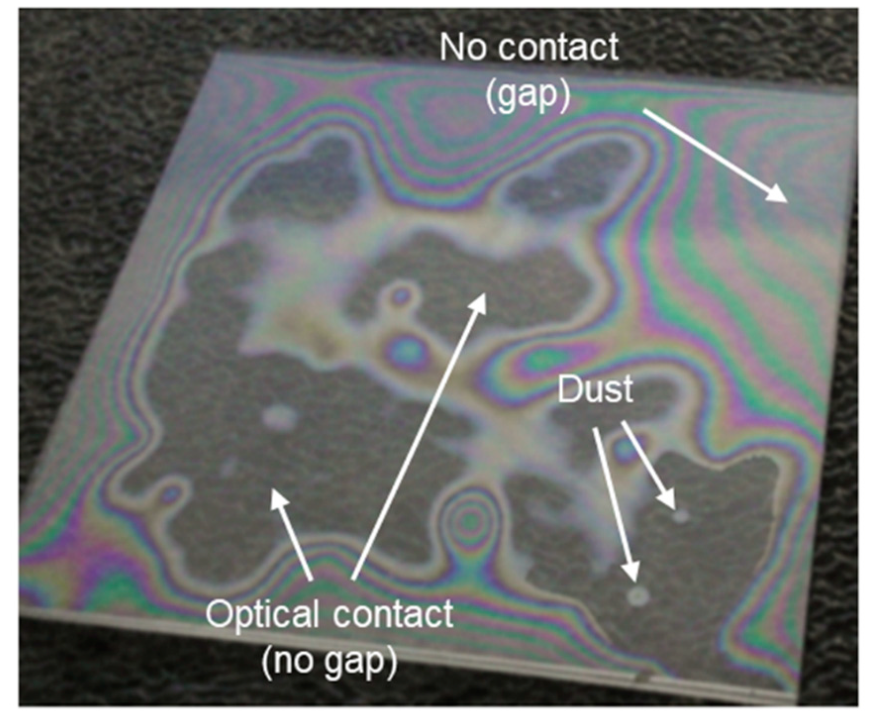
3.2. Calibration of the Laser Microwelding Process
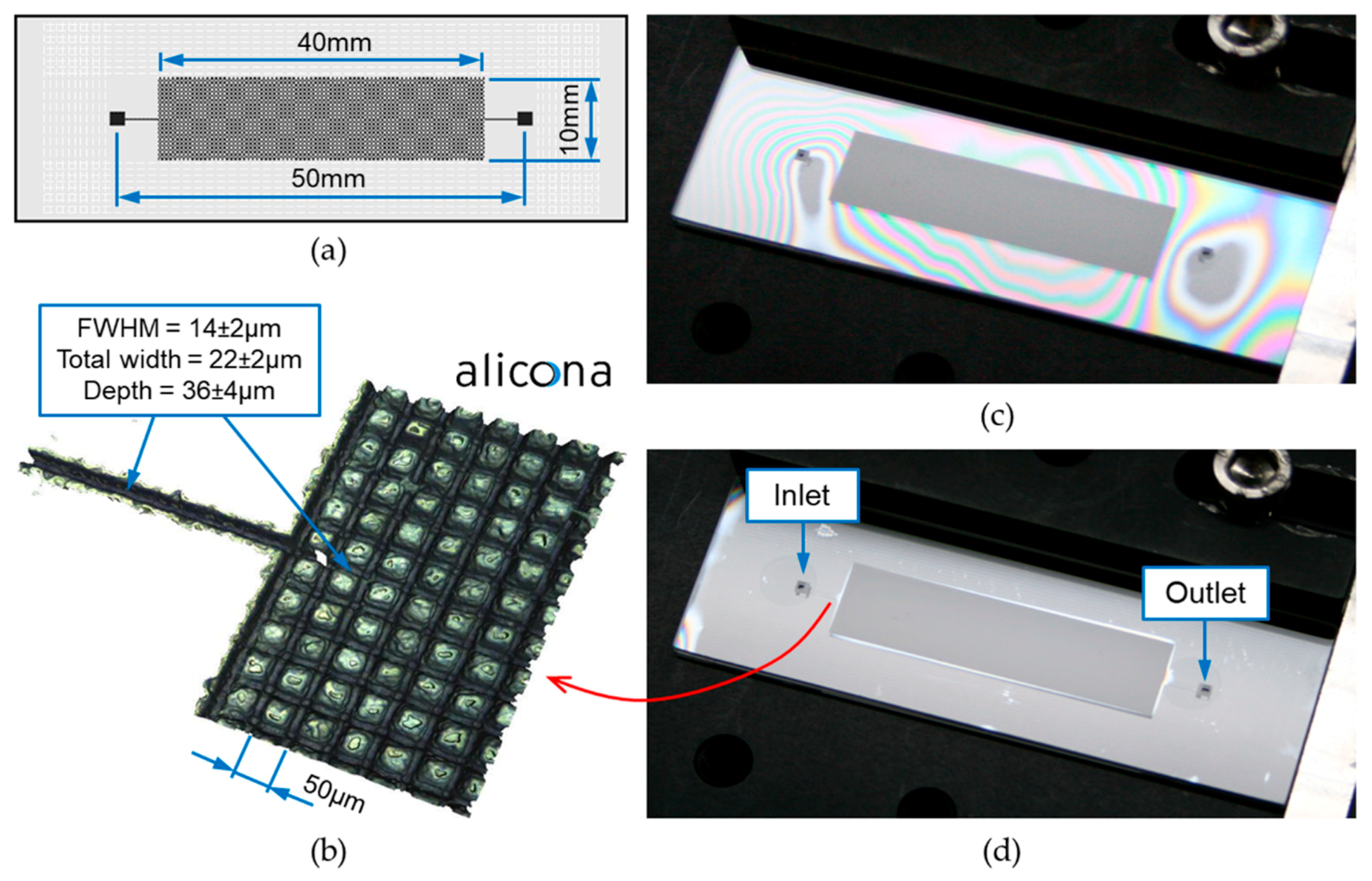
3.3. Manufacturing of Microfluidic Devices
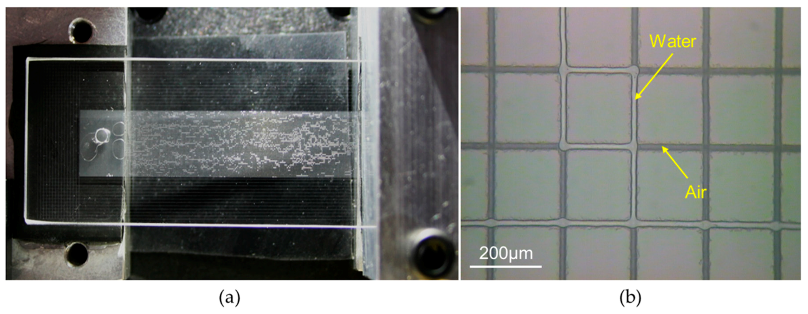
3.4. Fluid Flow Test
4. Conclusions
Supplementary Materials
Author Contributions
Funding
Conflicts of Interest
References
- Whitesides, G.M. The origins and the future of microfluidics. Nature 2006, 442, 368–373. [Google Scholar] [CrossRef] [PubMed]
- Sackmann, E.K.; Fulton, A.L.; Beebe, D.J. The present and future role of microfluidics in biomedical research. Nature 2014, 507, 181–189. [Google Scholar] [CrossRef] [PubMed]
- Watanabe, T.; Sassa, F.; Yoshizumi, Y.; Suzuki, H. Review of microfluidic devices for on-chip chemical sensing. Electron. Commun. Jpn. 2017, 100, 25–32. [Google Scholar] [CrossRef]
- Weibel, D.B.; Whitesides, G.M. Applications of microfluidics in chemical biology. Curr. Opin. Chem. Biol. 2006, 10, 584–591. [Google Scholar] [CrossRef] [PubMed]
- Riahi, R.; Tamayol, A.; Shaegh, S.A.M.; Ghaemmaghami, A.M.; Dokmeci, M.R.; Khademshosseini, A. Microfluidics for advanced drug delivery systems. Curr. Opin. Chem. Eng. 2015, 7, 101–112. [Google Scholar] [CrossRef]
- Nan, L.; Jiang, Z.; Wei, X. Emerging microfluidic devices for cell lysis: A review. Lab Chip 2014, 14, 1060–1073. [Google Scholar] [CrossRef] [PubMed]
- Faustino, V.; Catarino, S.O.; Lima, R.; Minas, G. Biomedical microfluidic devices by using low-cost fabrication techniques: A review. J. Biomech. 2016, 49, 2280–2292. [Google Scholar] [CrossRef] [PubMed] [Green Version]
- Bruijns, B.; van Asten, A.; Tiggelaar, R.; Gardeniers, H. Microfluidic devices for forensic DNA analysis: A review. Biosensors 2016, 6, 41. [Google Scholar] [CrossRef] [PubMed]
- Sajeesh, P.; Sen, A.K. Particle separation and sorting in microfluidic devices: A review. Microfluid. Nanofluid. 2014, 17, 1–52. [Google Scholar] [CrossRef]
- Karadimitriou, N.K.; Hassanizadeh, S.M. A review of micromodels and their use in two-phase flow studies. Vadose Zone J. 2012, 11. [Google Scholar] [CrossRef]
- Tsakiroglou, C.; Vizika-Kavvadias, O.; Lenormand, R. Use of Micromodels to Study Multiphase Flow in Porous Media. Available online: http://www.jgmaas.com/SCA/2013/SCA2013-038.pdf (accessed on 15 August 2018).
- Riazi, M.; Sohrabi, M.; Bernstone, C.; Jamiolahmady, M.; Ireland, S. Visualisation of mechanisms involved in CO2 injection and storage in hydrocarbon reservoirsand water-bearing aquifers. Chem. Eng. Res. Des. 2011, 89, 1827–1840. [Google Scholar] [CrossRef]
- Hu, R.; Wan, J.; Kim, Y.; Tokunaga, T.K. Wettability effects on supercritical CO2–brine immiscible displacement during drainage: Pore-scale observation and 3D simulation. Int. J. Greenh. Gas Contorl 2017, 60, 129–139. [Google Scholar] [CrossRef]
- Kim, Y.; Wan, J.; Kneafsey, T.J.; Tokunaga, T.K. Dewetting of silica surfaces upon reactions with supercritical CO2 and brine: Pore-scale studies in micromodels. Environ. Sci. Technol. 2012, 46, 4228–4235. [Google Scholar] [CrossRef] [PubMed]
- Bahralolom, I.M.; Bretz, R.E.; Orr, F.M. Experimental investigation of the interaction of phase behavior with microscopic heterogeneity in a CO2 flood. SPE Reserv. Eng. 1988, 3, 662–672. [Google Scholar] [CrossRef]
- Wang, Y.; Zhang, C.; Wei, N.; Oostrom, M.; Wietsma, T.W.; Li, X.; Bonneville, A. Experimental study of crossover from capillary to viscous fingering for supercritical CO2–water displacement in a homogeneous pore network. Environ. Sci. Technol. 2013, 47, 212–218. [Google Scholar] [CrossRef] [PubMed]
- Campbell, B.T.; Orr, F.M. Flow visualization for CO2/crude-oil displacements. Soc. Pet. Eng. J. 1985, 25, 665–678. [Google Scholar] [CrossRef]
- Van Dijke, M.I.J.; Sorbie, K.S.; Sohrabi, M.; Danesh, A. Simulation of WAG floods in an oil-wet micromodel using a 2-D pore-scale network model. J. Pet. Sci. Eng. 2006, 52, 71–86. [Google Scholar] [CrossRef]
- Sohrabi, M.; Danesh, A.; Tehrani, D.H.; Jamiolahmady, M. Microscopic mechanisms of oil recovery by near-miscible gas injection. Transp. Porous Media 2008, 72, 351–367. [Google Scholar] [CrossRef]
- Sohrabi, M.; Danesh, A.; Jamiolahmady, M. Visualisation of residual oil recovery by near-miscible gas and SWAG injection using high-pressure micromodels. Transp. Porous Media 2008, 74, 239–257. [Google Scholar] [CrossRef]
- Oostrom, M.; Mehmani, Y.; Romero-Gomez, P.; Tang, Y.; Liu, H.; Yoon, H.; Kang, Q.; Joekar-Niasar, V.; Balhoff, M.T.; Dewers, T.; et al. Pore-scale and continuum simulations of solute transport micromodel benchmark experiments. Comput. Geosci. 2016, 20, 857–879. [Google Scholar] [CrossRef]
- Goldenberg, L.C.; Hutcheon, I.; Wardlaw, N. Experiments on transport of hydrophobic particles and gas bubbles in porous media. Transp. Porous Media 1989, 4, 129–145. [Google Scholar] [CrossRef]
- Leester-Schädel, M.; Lorenz, T.; Jürgens, F.; Richter, C. Fabrication of microfluidic devices. In Microsystems for Pharmatechnology; Dietzel, A., Ed.; Springer: New York, NY, USA, 2016; pp. 23–57. [Google Scholar]
- Iliescu, C.; Taylor, H.; Avram, M.; Miao, J.; Franssila, S. A practical guide for the fabrication of microfluidic devices using glass and silicon. Biomicrofluidics 2012, 6, 016505. [Google Scholar] [CrossRef] [PubMed]
- Queste, S.; Salut, R.; Clatot, S.; Rauch, J.-Y.; Khan Malek, C.G. Manufacture of microfluidic glass chips by deep plasma etching, femtosecond laser ablation, and anodic bonding. Microsyst. Technol. 2010, 16, 1485–1493. [Google Scholar] [CrossRef]
- Khan Malek, C.G. Laser processing for bio-microfluidics applications (part I). Anal. Bioanal. Chem. 2006, 385, 1351–1361. [Google Scholar] [CrossRef] [PubMed]
- Khan Malek, C.G. Laser processing for bio-microfluidics applications (part II). Anal. Bioanal. Chem. 2006, 385, 1362–1369. [Google Scholar] [CrossRef] [PubMed]
- Yen, M.-H.; Cheng, J.-Y.; Wei, C.-W.; Chuang, Y.-C.; Young, T.-H. Rapid cell-patterning and microfluidic chip fabrication by crack-free CO2 laser ablation on glass. J. Micromech. Microeng. 2006, 16, 1143–1153. [Google Scholar] [CrossRef]
- Nikumb, S.; Chen, Q.; Li, C.; Reshef, H.; Zheng, H.Y.; Qiu, H.; Low, D. Precision glass machining, drilling and profile cutting by short pulse lasers. Thin Solid Films 2005, 477, 216–221. [Google Scholar] [CrossRef] [Green Version]
- Darvishi, S.; Cubaud, T.; Longtin, J.P. Ultrafast laser machining of tapered microchannels in glass and PDMS. Opt. Laser. Eng. 2012, 50, 210–214. [Google Scholar] [CrossRef]
- Fu, L.-M.; Ju, W.-J.; Yang, R.-J.; Wang, Y.-N. Rapid prototyping of glass-based microfluidic chips utilizing two-pass defocused CO2 laser beam method. Microfluid. Nanofluid. 2013, 14, 479–487. [Google Scholar] [CrossRef]
- Gomez, D.; Goenaga, I.; Lizuain, I.; Ozaita, M. Femtosecond laser ablation for microfluidics. Opt. Eng. 2005, 44, 051105. [Google Scholar] [CrossRef]
- Sugioka, K.; Cheng, Y. Fabrication of 3D microfluidic structures inside glass by femtosecond laser micromachining. Appl. Phys. A 2014, 114, 215–221. [Google Scholar] [CrossRef]
- Serhatlioglu, M.; Ortaç, B.; Elbuken, C.; Biyikli, N.; Solmaz, M.E. CO2 laser polishing of microfluidic channels fabricated by femtosecond laser assisted carving. J. Micromech. Microeng. 2016, 26, 115011. [Google Scholar] [CrossRef]
- Bellouard, Y.; Said, A.; Dugan, M.; Bado, P. Fabrication of high-aspect ratio, micro-fluidic channels and tunnels using femtosecond laser pulses and chemical etching. Opt. Express 2004, 12, 2120–2129. [Google Scholar] [CrossRef] [PubMed]
- Matsuo, S.; Sumi, H.; Kiyama, S.; Tomita, T.; Hashimoto, S. Femtosecond laser-assisted etching of Pyrex glass with aqueous solution of KOH. Appl. Surf. Sci. 2009, 255, 9758–9760. [Google Scholar] [CrossRef]
- Gottmann, J.; Hermans, M.; Ortmann, J. Digital photonic production of micro structures in glass by in-volume selective laser-induced etching using a high speed micro scanner. Phys. Procedia 2012, 39, 534–541. [Google Scholar] [CrossRef]
- Gottmann, J.; Hermans, M.; Repiev, N.; Ortmann, J. Selective laser-induced etching of 3D precision quartz glass components for microfluidic applications—Up-scaling of complexity and speed. Micromachines 2017, 8. [Google Scholar] [CrossRef]
- Wlodarczyk, K.L.; MacPherson, W.M.; Hand, D.P. Laser Processing of Borofloat®33 Glass. Available online: https://researchportal.hw.ac.uk/en/publications/laser-processing-of-borofloat33-glass (accessed on 15 August 2018).
- Wlodarczyk, K.L.; Brunton, A.; Rumsby, P.; Hand, D.P. Picosecond laser cutting and drilling of thin flex glass. Opt. Lasers Eng. 2016, 78, 64–74. [Google Scholar] [CrossRef]
- Carter, R.M.; Chen, J.; Shephard, J.D.; Thomson, R.R.; Hand, D.P. Picosecond laser welding of similar and dissimilar materials. Appl. Opt. 2014, 53, 4233–4238. [Google Scholar] [CrossRef] [PubMed]
- Chen, J.; Carter, R.M.; Thomson, R.R.; Hand, D.P. Avoiding the requirement for pre-existing optical contact during picosecond laser glass-to-glass welding. Opt. Express 2015, 23, 18645–18657. [Google Scholar] [CrossRef] [PubMed]
- Borofloat®33—Borosilicate Glass. Available online: https://www.schott.com/borofloat/english/ (accessed on 11 Jun 2018).
- Rabbani, H.S.; Or, D.; Liu, Y.; Lai, C.-Y.; Lu, N.B.; Datta, S.S.; Stone, H.A.; Shokri, N. Suppressing viscous fingering in structured porous media. Proc. Natl. Acad. Sci. USA 2018, 115, 4833–4838. [Google Scholar] [CrossRef] [PubMed]


| Wavelength (nm) | P (W) | Ep (μJ) | 2 ω0 (μm) | M2 (value) | F (J/cm2) 1 |
|---|---|---|---|---|---|
| 1030 | 50 | 125 | 35 ± 1 | 1.3 ± 0.1 | 26.0 ± 1.5 |
| 515 | 30 | 75 | 21 ± 1 | 1.4 ± 0.1 | 36.3 ± 3.5 |
| 343 | 18 | 45 | 20 ± 1 | 2.1 ± 0.1 | 28.9 ± 2.9 |
© 2018 by the authors. Licensee MDPI, Basel, Switzerland. This article is an open access article distributed under the terms and conditions of the Creative Commons Attribution (CC BY) license (http://creativecommons.org/licenses/by/4.0/).
Share and Cite
Wlodarczyk, K.L.; Carter, R.M.; Jahanbakhsh, A.; Lopes, A.A.; Mackenzie, M.D.; Maier, R.R.J.; Hand, D.P.; Maroto-Valer, M.M. Rapid Laser Manufacturing of Microfluidic Devices from Glass Substrates. Micromachines 2018, 9, 409. https://doi.org/10.3390/mi9080409
Wlodarczyk KL, Carter RM, Jahanbakhsh A, Lopes AA, Mackenzie MD, Maier RRJ, Hand DP, Maroto-Valer MM. Rapid Laser Manufacturing of Microfluidic Devices from Glass Substrates. Micromachines. 2018; 9(8):409. https://doi.org/10.3390/mi9080409
Chicago/Turabian StyleWlodarczyk, Krystian L., Richard M. Carter, Amir Jahanbakhsh, Amiel A. Lopes, Mark D. Mackenzie, Robert R. J. Maier, Duncan P. Hand, and M. Mercedes Maroto-Valer. 2018. "Rapid Laser Manufacturing of Microfluidic Devices from Glass Substrates" Micromachines 9, no. 8: 409. https://doi.org/10.3390/mi9080409