
Low Noise Low Power CMOS Telescopic-OTA for Bio-Medical Applications

Abstract
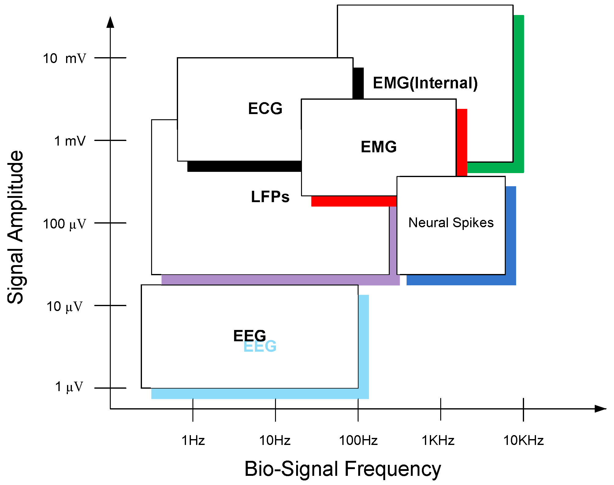
:1. Introduction
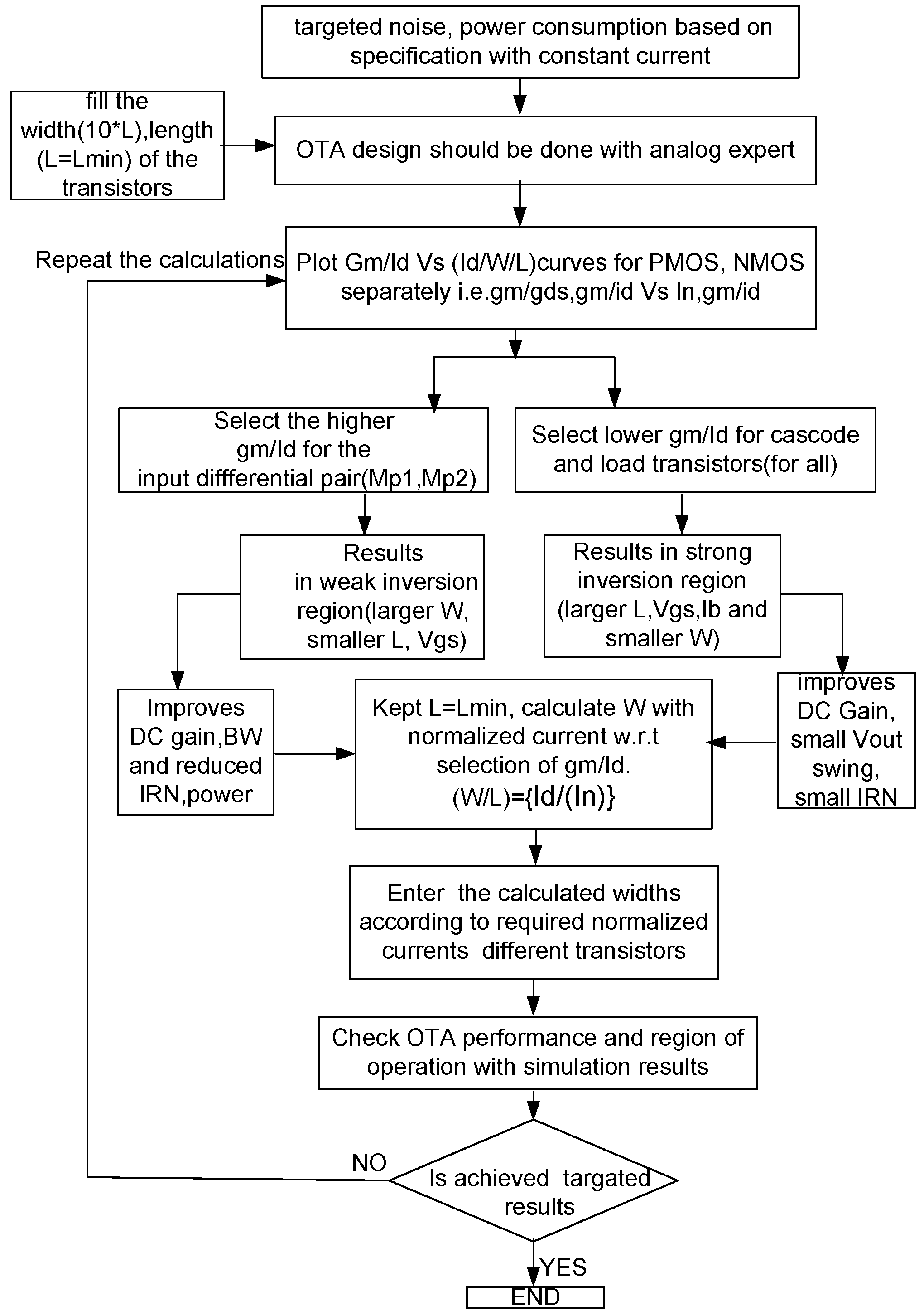
2. / Methodology
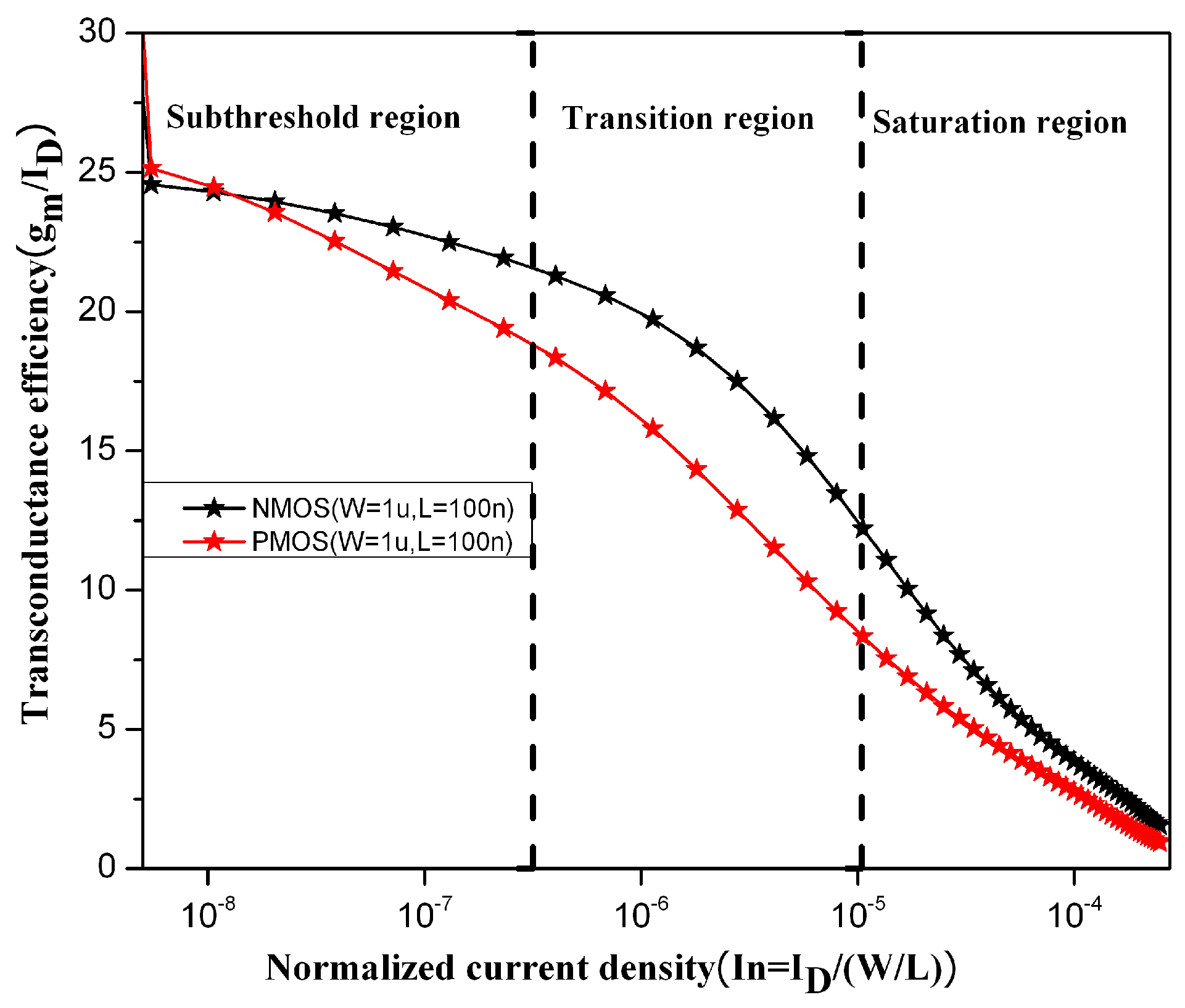
- The selection of a low / value from Figure 3 for reducing the input referred noise, ensures high , lower W and larger L, without current reduction. This means that the load and stealing transistors , operate in strong inversion.
- For cascode transistors , a moderate value of / is selected with respect to the curves to ensure operates in moderate inversion. With allowable cost of voltage swing, the cascode transistors are introduced to improve the gain of preamplifier without further noise inclusion by shielding property [10].
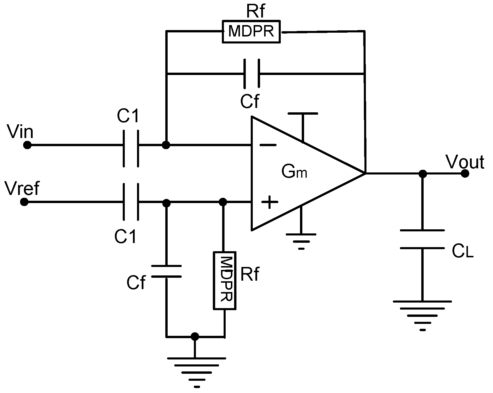
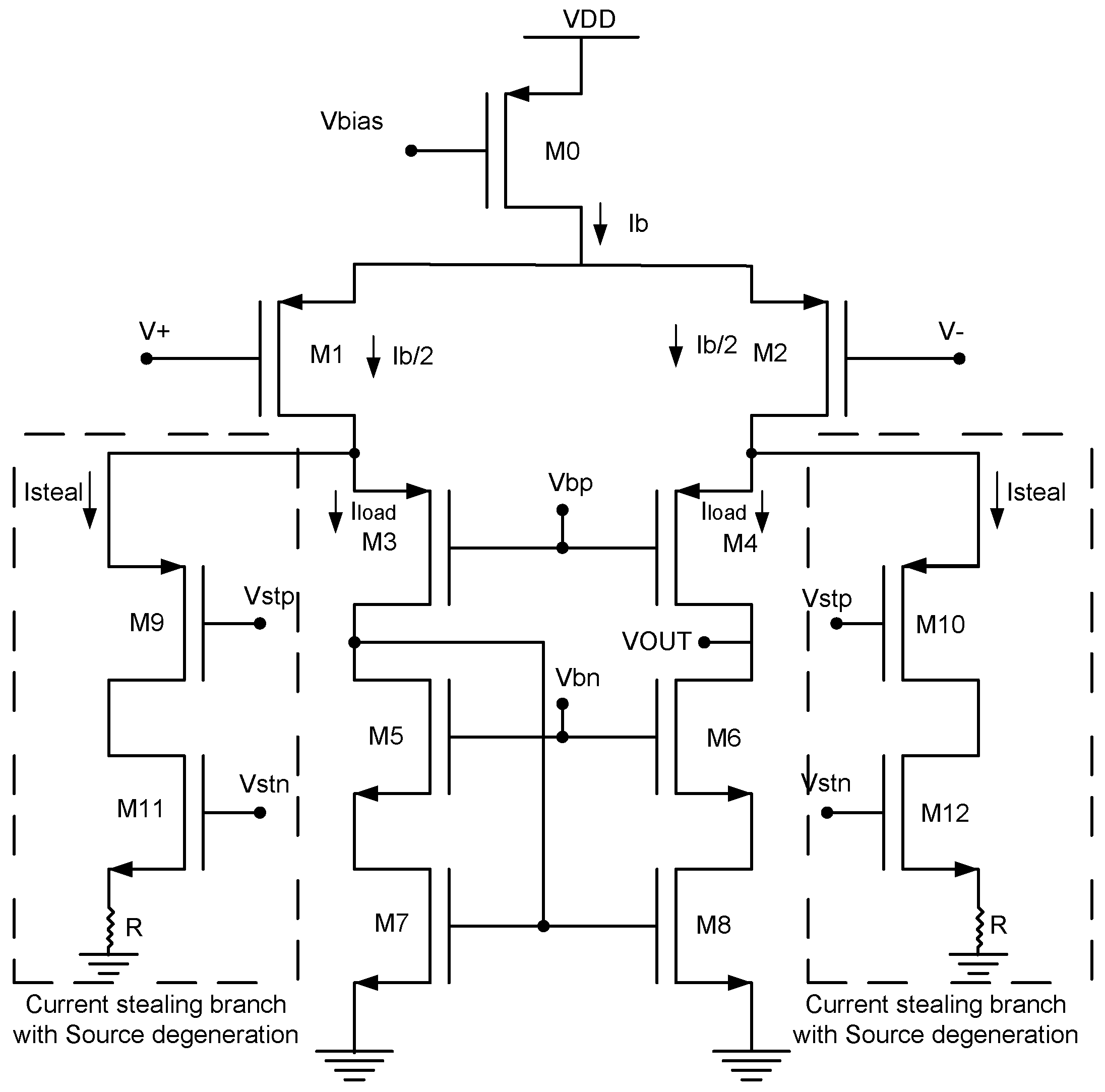
3. Design of Telescopic OTA
4. Proposed Low Noise OTA Design
- = Thermal voltage (KT/q) = 26 mV,
- = Oxide Capacitance per unit area,
- µ = Mobility of charge carriers,
- k = Subthreshold gate coupling coefficient (Typically, 0.7) and
- = Aspect ratio of transistor.
- = Input referred noise voltage,
- = Total bias current,
- = Thermal voltage,
- = Boltzman constant,
- = Bandwidth in Hz.
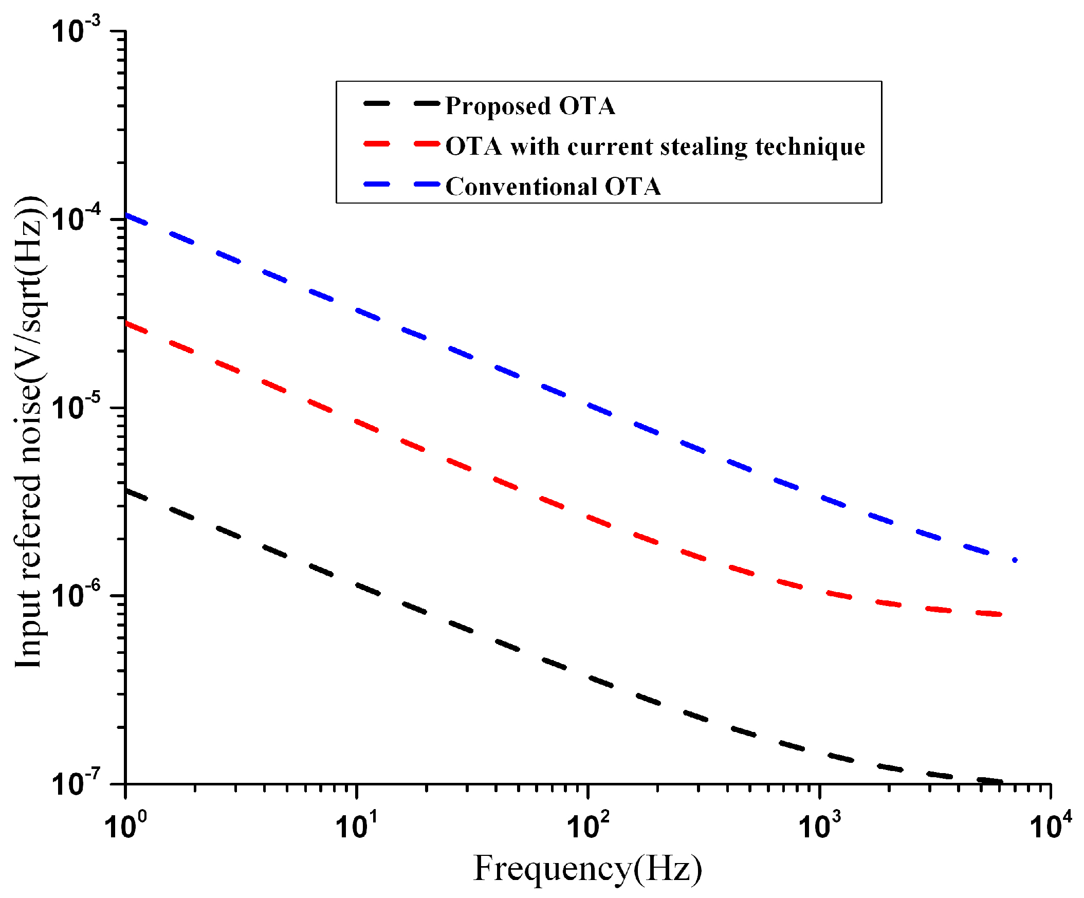
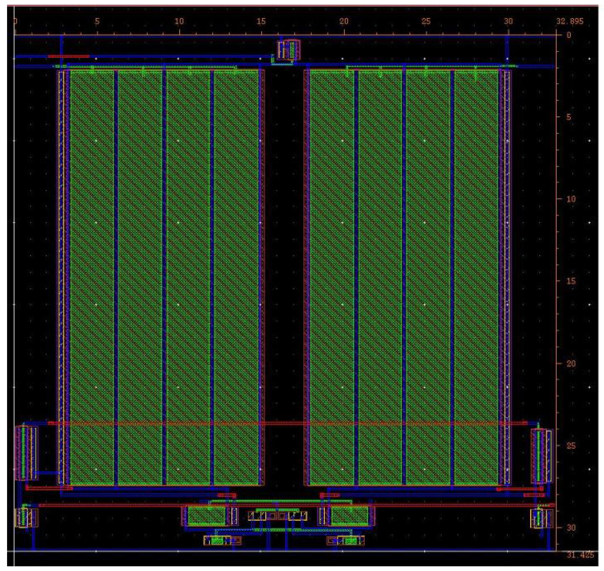
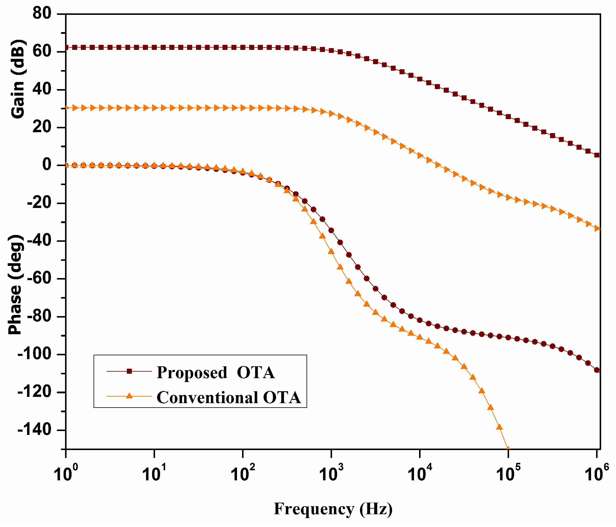
5. Simulation and Post Layout Results
6. Conclusions
Acknowledgments
Author Contributions
Conflicts of Interest
Abbreviations
| NEMS/MEMS | Nano Electro Mechanical System / Micro Electro Mechanical System |
| EEG | Electroencephalogram |
| MOS | Metal Oxide Semiconductor |
| DC | Direct Current |
| UGB | Unity Gain Bandwidth |
| CMRR | Common Mode Rejection Ratio |
| PSD | Power Spectral density |
References
- Harrison, R.R.; Charles, C.A. low-power low-noise CMOS amplifier for neural recording applications. IEEE J. Solid-State Circuits 2003, 38, 958–965. [Google Scholar] [CrossRef]
- Chaturvedi, V.; Amrutur, B. A Low-Noise Low-Power Noise-Adaptive Neural Amplifier in 0.13 um CMOS Technology. In Proceedings of the 24th International Conference on VLSI Design, Chennai, India, 2–7 January 2011; pp. 328–333.
- Liu, L.; Zou, X.; Goh, W.L.; Ramamoorthy, R.; Dawe, G.; Je, M. 800 nW 43 nV/ neural recording amplifier with enhanced noise efficiency factor. Electron. Lett. 2012, 48, 479–480. [Google Scholar] [CrossRef]
- Shoaran, M.; Pollo, C.; Leblebici, Y.; Schmid, A. Design techniques and analysis of high-resolution neural recording systems targeting epilepsy focus localization. In Proceedings of the the IEEE Annual International Conference of Engineering in Medicine and Biology Society (EMBC), San Diego, CA, USA, 28 August–1 September 2012; pp. 5150–5153.
- Yang, T.; Holleman, J. An Ultra low-Power Low-Noise CMOS Biopotential Amplifier for Neural Recording. IEEE Trans. Circuits Syst. II Express Br. 2015, 62, 927–931. [Google Scholar] [CrossRef]
- Nemirovsky, Y.; Brouk, I.; Jakobson, C. 1/f noise in CMOS transistors for analog applications. IEEE Trans. Electron Devices 2001, 48, 921–927. [Google Scholar] [CrossRef]
- Girardi, A.; Severo, L.C. gm/ID Design methodology. In Analog CMOS Design Automation Methodologies for Low-Power Applications; InTech: Rijeka, Croatia, 2011; pp. 32–58. [Google Scholar]
- Akbari, M.; Hashemipour, O. Design and analysis of folded cascode OTAs using Gm/Id methodology based on flicker noise reduction. Analog Integr. Circuits Signal Process. 2015, 83, 343–352. [Google Scholar] [CrossRef]
- Akbari, M.; Shokouhifar, M.; Hashemipour, O.; Jalali, A.; Hassanzadeh, A. Systematic design of analog integrated circuits using ant colony algorithm based on noise optimization. Analog Integr. Circuits Signal Process. 2016, 86, 327–339. [Google Scholar] [CrossRef]
- Razavi, B. Single stage amplifiers. In Design of Analog CMOS Integrated Circuits, 1st ed.; McGraw-Hill, Inc.: New York, NY, USA, 2002; pp. 89–90. [Google Scholar]
- Kumaravel, S.; Bharadwaj, K.N.; Venkataramani, B.; Raja, R. A Power Efficient Low Noise Preamplifier for Bio-Medical Applications. J. Low Power Electron. 2013, 9, 501–509. [Google Scholar] [CrossRef]
- Carusone, T.C.; Johns, D.; Martin, K. Analog integrated circuit biasing. In Analog Integrated Circuit Design, 2nd ed.; John Wiley & Sons: Hoboken, NJ, USA, 2011; pp. 303–305. [Google Scholar]
- Layton, K.D. Low Voltage Analog CMOS Architectures and Design Methods. Available online: http://scholarsarchive.byu.edu/etd/1218/ (accessed on 21 October 2016).
- Tsividis, Y.; McAndrew, C. Inversion. In Operation and Modeling of the MOS Transistor; Oxford Series in Electrical and Computer Engineering; Oxford University Press: New York, NY, USA, 2011; pp. 64–78. [Google Scholar]
- Martegani, R.F. An All-Inversion-Region gm/Id Based Design Methodology for Radio frequency Blocks in Cmos Nanometer Technologies. Available online: http://digital.csic.es/bitstream/10261/85749/1/tesisFiorelli.pdf (accessed on 21 October 2016).
- Joye, N.; Schmid, A.; Leblebici, Y. Electrical modeling of the cell electrode interface for recording neural activity from high-density micro electrode arrays. Neuro computing 2009, 73, 250–259. [Google Scholar]
- Enz, C.; Krummenacher, F.; Vittoz, E. An analytical mos transistor model valid in all regions of operation and dedicated to low-voltage and low-current applications. Analog Integr. Circuits Signal Process. 1995, 8, 83–114. [Google Scholar] [CrossRef]
- Qian, C.; Parramon, J.; Sanchez-Sinencio, E. A micropower low-noise neural recording front-end circuit for epileptic seizure detection. IEEE J. Solid-State Circuits 2011, 51, 1392–1405. [Google Scholar] [CrossRef]
- Enz, C.; Temes, G. Circuit techniques for reducing the effects of op-amp imperfections: Autozeroing, correlated double sampling, and chopper stabilization. Proc. IEEE 1996, 84, 1584–1614. [Google Scholar] [CrossRef]
- Ou, J.; Ferreira, P. A gm/ID based noise optimization for cmos folded-cascode operational amplifier. IEEE Trans. Circuits Syst. II Express Br. 2014, 61, 783–787. [Google Scholar] [CrossRef]
- Ulbert, I.; Heit, G.; Madsen, J.; Karmos, G.; Halgren, E. Laminar analysis of human neocortical interictal spike generation and propagation: Current source density and multiunit analysis in vivo. Epilepsia 2004, 45, 48–56. [Google Scholar] [CrossRef] [PubMed]
- Mohseni, P.; Najafi, K. A fully integrated neural recording amplifier with DC input stabilization. IEEE Trans. Bio-Med. Eng. 2004, 51, 832–837. [Google Scholar] [CrossRef] [PubMed]


| Inversion Coefficient (IC) | Relation between , | Inversion Level | Region of Operation |
|---|---|---|---|
| IC > 10 | Strong inversion | Saturation region | |
| 10 > IC > 0.1 | overestimate | Moderate inversion | Middle region |
| IC < 0.1 | Weak inversion | Subthreshold region |
| Devices | W/L | |||
|---|---|---|---|---|
| M0 | 900 n/130 n | 35 | 22 | 1.6 µ |
| M1, M2 | 80 µ/6 µ | 21.28 | 26 | 800 n |
| M3, M4 | 900 n/2.2 µ | 1.97 | 21 | 90 n |
| M5, M6 | 120 n/100 n | 1.90 | 20 | 90 n |
| M7, M8 | 120 n/100 n | 1.933 | 21 | 90 n |
| M9, M10 | 3 µ/100 n | 19.6 | 17 | 710 n |
| M11, M12 | 820 n/100 n | 16 | 17 | 710 n |
| Parameter | [8] | [1] | [2] | [5] | This Work |
|---|---|---|---|---|---|
| Technology (µm) | 0.18 | 1.5 | 0.13 | 0.09 | 0.09 |
| (V) | ±1.8 | ±2.5 | 1.5 | 1 | 1.2 |
| current (µA) | - | 0.128 | - | 2.85 | 1.6 |
| Gain (dB) | 60.8 | 40 | 39.4 | 58.7 | 62 |
| Power (µW) | 720 | 0.32 | 1.5 | 2.85 | 1.9 |
| Input referred noise (µVrms) | 61.5 | 2.4 | 5.5 | 3.04 | 3.2 |
| CMRR (dB) | - | 88 | - | - | 78 |
| NEF | - | 6 | - | 1.93 | 1.86 |
| NEF. | - | 90 | - | 4.151 | |
| Area (µm | - | - | - | - | 258.43 |
© 2016 by the authors; licensee MDPI, Basel, Switzerland. This article is an open access article distributed under the terms and conditions of the Creative Commons Attribution (CC-BY) license (http://creativecommons.org/licenses/by/4.0/).
Share and Cite
Saidulu, B.; Manoharan, A.; Sundaram, K. Low Noise Low Power CMOS Telescopic-OTA for Bio-Medical Applications. Computers 2016, 5, 25. https://doi.org/10.3390/computers5040025
Saidulu B, Manoharan A, Sundaram K. Low Noise Low Power CMOS Telescopic-OTA for Bio-Medical Applications. Computers. 2016; 5(4):25. https://doi.org/10.3390/computers5040025
Chicago/Turabian StyleSaidulu, Bellamkonda, Arun Manoharan, and Kumaravel Sundaram. 2016. "Low Noise Low Power CMOS Telescopic-OTA for Bio-Medical Applications" Computers 5, no. 4: 25. https://doi.org/10.3390/computers5040025