Article

A Zero-Power, Low-Cost Ultraviolet-C Colorimetric Sensor Using a Gallium Oxide and Reduced Graphene Oxide Hybrid via Photoelectrochemical Reactions

1
Department of Materials Engineering, Korea Aerospace University, Goyang 10540, Korea
2
Electronic Materials and Device Research Center, Korea Electronics Technology Institute, Seongnam 13509, Korea
3
Department of Cogno-Mechatronics Engineering, Pusan National University, Busan 46241, Korea
*
Authors to whom correspondence should be addressed.
Catalysts 2017, 7(9), 248; https://doi.org/10.3390/catal7090248
Submission received: 5 July 2017 / Revised: 12 August 2017 / Accepted: 23 August 2017 / Published: 24 August 2017

Abstract

:
A zero-power, low-cost ultraviolet (UV)-C colorimetric sensor is demonstrated using a gallium oxide and reduced graphene oxide (rGO) hybrid via photoelectrochemical reactions. A wide bandgap semiconductor (WBS) such as gallium oxide with an energy bandgap of 4.9 eV generates electron-hole pairs (EHPs) when exposed under a mercury lamp emitting 254 nm. While the conventional UVC sensors employing WBS convert the generated EHPs into an electrical signal via a solid-state junction device (SSD), our newly proposed UVC sensory system works by converting EHPs into an electrochemical reaction. The electrochemical reaction causes the degradation of a cationic thiazine redox dye, methylene blue (MB) and thereby spontaneously changes its color. As more rGO was hybridized with the gallium oxide, MB degradation was effectively expedited. Thus, the level of MB degradation under UVC can be evaluated as a UVC indicator. Unlike conventional SSD-based UVC sensors, our responsive colorimetric sensor can be applied where needed inexpensively and zero power.

Graphical Abstract

1. Introduction

Over the past three decades, awareness of—and concern regarding—ultraviolet (UV) light has grown, particularly as researchers identified correlations between skin diseases and UV exposure [1]. UV light is an electromagnetic radiation spectrum between X-rays and visible light, and is divided into UVA (320–400 nm), UVB (290–320 nm) and UVC (220–290 nm), depending on its energy [2]. Shorter wavelengths lead to greater energy output, producing greater chemical bond breakage and an increase in the ionization of atoms and molecules upon exposure [3]. Both UVA and UVB penetrate the atmosphere and cause photochemical damage to skin and eyes [1,4]. As such, UVA and UVB sensors, and their protection-related applications, have been intensively explored [5]. However, UVC exposure and its measurement have garnered less attention, because UVC is strongly attenuated by the ozone layer and no significantly harmful effects on humans have been reported [2]. More recently, humans have become susceptible to UVC radiation, not from the sun, but from commonly used consumer devices [5,6,7]. For example, germicidal lamps emitting UVC are widely used, especially in hospitals and homes, to kill harmful bacteria, viruses, mold, dust and mites [8]. Even smaller amounts of UVC exposure from these lamps without proper protection can induce serious damage to the DNA in the skin and eyes. Despite this, UVC sensors have only been used in limited areas and applications, primarily due to their high production and operating costs. While traditional UV sensors were made of photomultiplier tubes that required bulky and heavy components [9], modern UV detectors and sensors are usually solid-state devices (SSDs) employing semiconductors. Photons incident on the surface of the semiconductor can create electron-hole pairs (EHPs) that lead to an electric signal [10]. Very recently, Ga2O3 with an energy bandgap of about 4.9 eV has been investigated as a potential UVC detector to replace other wide bandgap semiconductors (WBSes) such as SiC, GaN, and GaAlN [9,10,11,12]. In particular, research has shown that the Ga2O3 -based detector has a spectral response with solar-blind (visible-blind) sensitivity [13]. However, the preparation of Ga2O3 and the process integration technology that uses WBSes suffer from excessive costs and high operating power consumption [14]. Thus, new types of UVC sensors are required to overcome the challenges of the current UVC sensor market and fulfill public demand. In this study, a low-cost, zero-power UVC sensor composed of a gallium oxide and reduced graphene oxide (rGO) hybrid is presented. Unlike conventional UVC sensors operating via solid-state junction physics, the proposed UVC sensor works via photoelectrochemical reactions. It can also be applied to structural components to monitor maintenance periods, which can greatly reduce operating costs. Only incident photons larger than the bandgap of a semiconductor can generate EHPs in a semiconductor. In other words, the presence of EHP generation in semiconductors can provide information about the incident photon energy. For example, EHPs are generated upon UVA and UVB irradiation into TiO2, because the incident photon energy is larger than the bandgap of TiO2. However, an identical incident photon transmits into Ga2O3 materials, because the incident photon energy is smaller than the energy gap of Ga2O3, as shown in Figure 1a. It is worthwhile correlating the energy bandgap of a semiconductor with photoelectrochemical reactions, since the proposed UVC sensor works by converting EHP generation into photoelectrochemical reactions, unlike conventional SSDs, which convert EHPs into electrical signals. Figure 1b shows energy bandgaps for various semiconductors, including WBSes such as SiC, GaN and Ga2O. In addition, the energy band diagram for the various semiconductors is correlated with the redox potential for water splitting. If the incident photon energy is larger than the bandgap of semiconductors, and the bottom edge of the conduction band is located more negative than the redox potential (H2/H2O), water molecules are reduced by the photon-generated electrons, and H2 can be generated from the H2O.
In the same way, if the incident photon energy is larger than that of the semiconductor and the top edge of the valence band is located more positive level (H2O/O2), water molecules are oxidized by the photon-generated holes, and O2 can be generated from the H2O. This mechanism is called water splitting, and the reaction can be used to indicate UVC irradiation, because Ga2O3 in the 4.9-eV bandgap absorbs the UVC, generates EHPs and fulfills the requirements of the above water splitting reaction. The photocatalytic reaction, which is the main mechanism for the UVC sensor in this work, occurs only on the surface of the material. Thus, sensor resolution and responsibility are highly dependent on the surface area, and can be enhanced by increasing the surface area where the photocatalytic reaction takes place. Since the discovery of graphene [17], which is an allotrope of carbon in the form of an atomic-scale honeycomb structure, various other two-dimensional (2D) materials, including graphene oxide (GO) and reduced graphene oxide (rGO), have been investigated intensively due to their superior surface-to-volume ratios [17]. The rich surface characteristics of GO and rGO are highly attractive because they can enhance the stimuli-responsive surface reactions. Recently, it was reported that the incorporation of GO into Ga2O3 significantly enhanced photocatalytic reactions under UV irradiation [18]. The same study demonstrated that a photocatalytic reaction with hybrid composites (HCs) increased as the GO increased in the HCs.

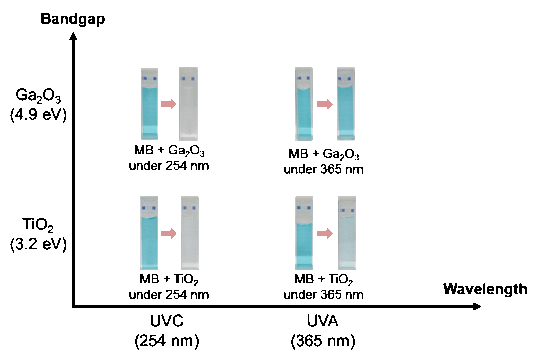
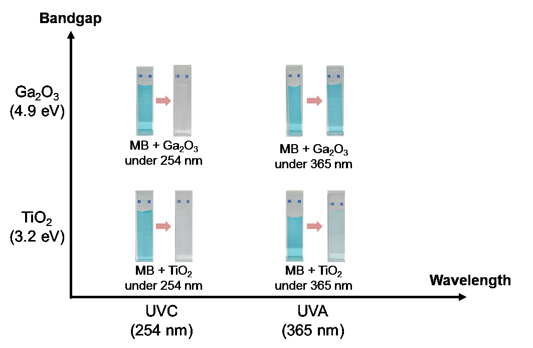
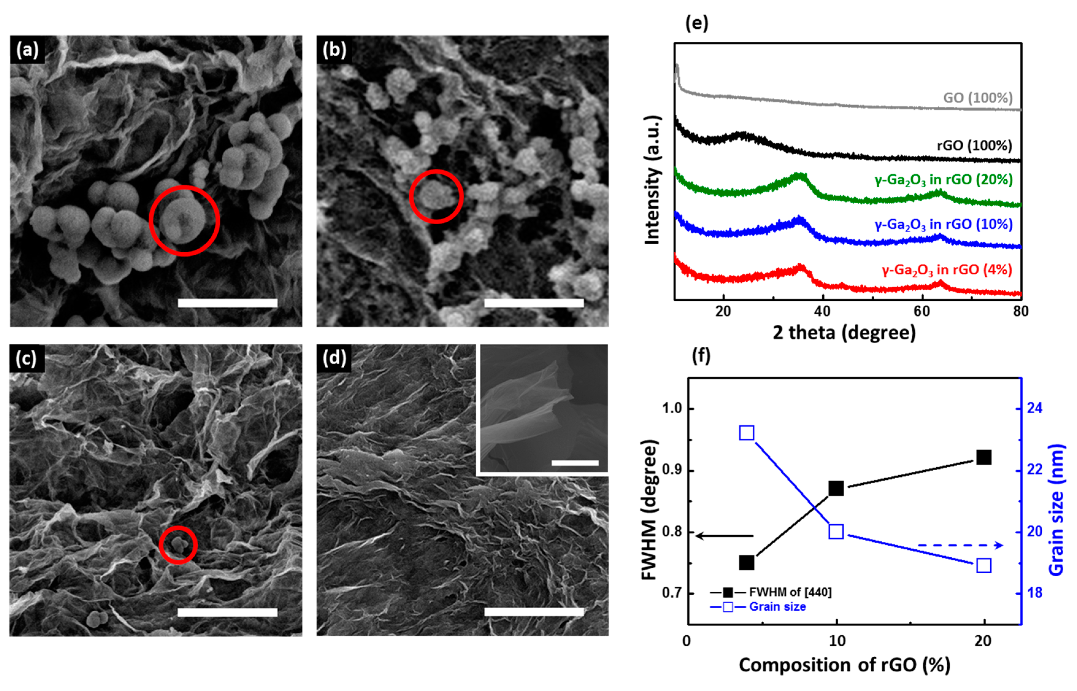
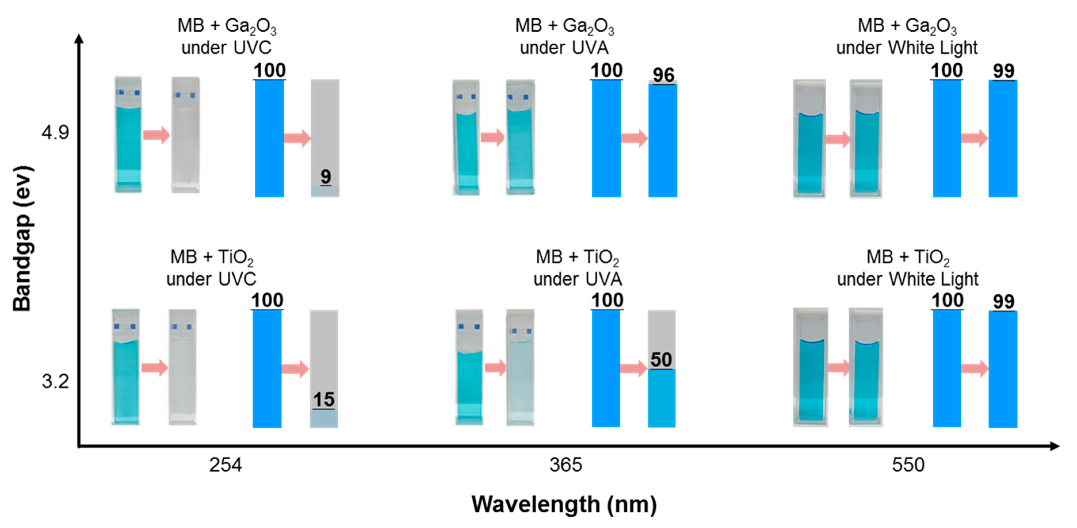
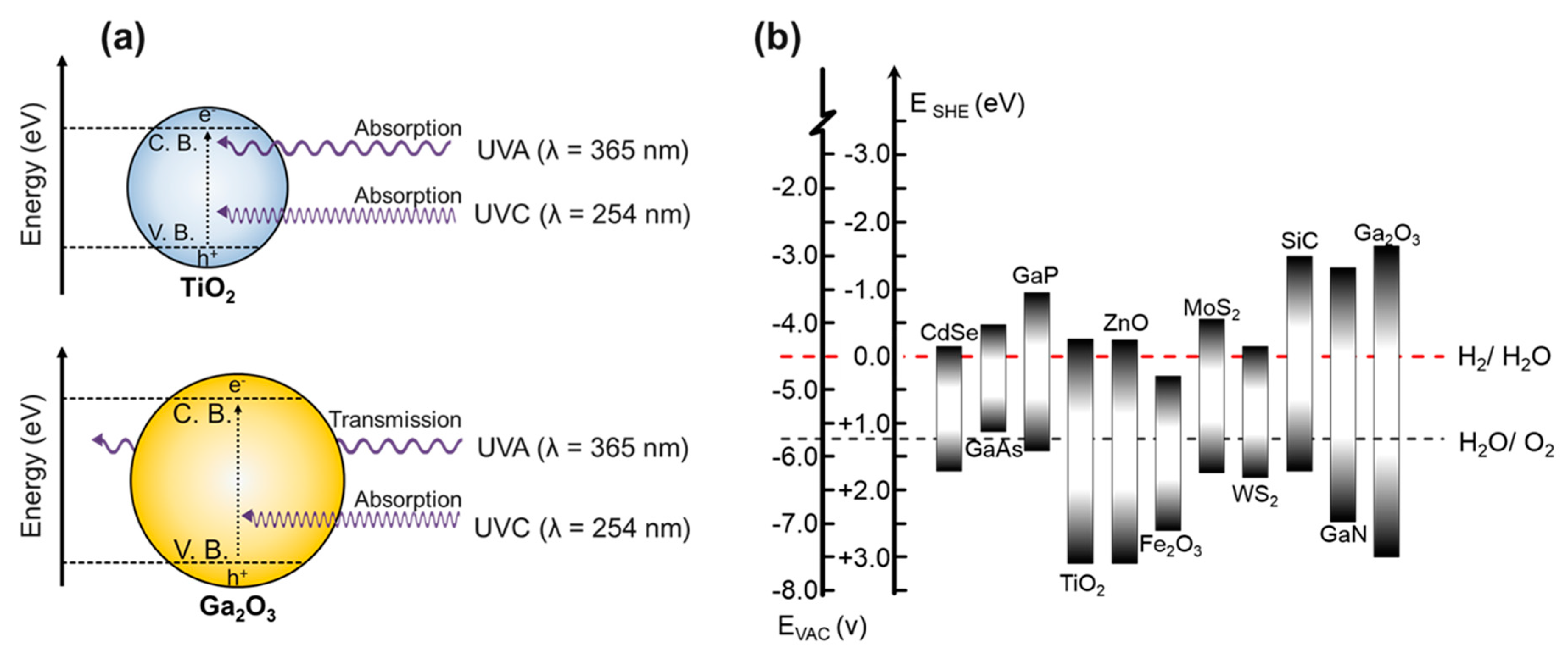
2. Results and Discussion

Various HCs formed, and their physical properties were investigated, as shown in Figure 2. It was found that less Ga2O3 formed with a greater rGO ratio, as shown in Figure 2a–c, and no Ga2O3 was observed with 100% rGO, as shown in Figure 2d. The HCs formed were analyzed via XRD spectra to investigate structure formation. The results showed that γ-Ga2O3 were preferably formed, and that the crystallinity of the Ga2O3 remained unchanged, regardless of rGO ratio. Furthermore, grain sizes of the γ-Ga2O3 in the HCs were extracted using the full-width at half-maximum (FWHM) method through the XRD diffraction patterns as appeared in Figure 2e. The Ga2O3 grain size (~23 nm) continued to decrease as the rGO concentration increased in the HCs, and it dropped below 20 nm at 20% rGO. As previously discussed [17], the functional groups at the rGO surface could serve as nucleation sites and finally affected the grain size of the Ga2O3 in the HCs.
The photoelectrochemical reaction upon UVC irradiation was systemically quantified through the MB degradation. The effects of the rGO ratio in the HCs on the MB degradation are shown in Figure 3; the relative concentration of MB with HCs decreased with time, and the degradation level was accelerated with higher rGO ratios in the HCs. The enhanced photoelectrochemical reaction via the HCs was well described in the previous study [18]. In short, the generated electron-hole pairs in the Ga2O3 under the UVC irradiation spread out through the rGO in a relatively high mobility value, which increased the lifetime of electron-hole pairs and significantly enhanced the photocatalytic reactions with the MB. This photocatalytic reaction with the MB was reflected by the apparent color change of the MB depending on the UVC exposure time, which will be discussed next.
Figure 4 shows a schematic matrix for the UVC sensor application via the photoelectrochemical reaction of Ga2O3 and TiO2 based nanomaterials. Under the visible spectrum radiation (white light), both the MB (Ga2O3) and the MB (TiO2) retained their blue color. This was because Ga2O3 and TiO2 were transparent at visible radiation and no EPHs were generated. However, TiO2, with an energy bandgap of 3.2 eV, generated EPHs upon UVA exposure, and thereby caused photoelectrochemical reactions in the MB (TiO2), which turned the blue to white. In contrast, the MB (Ga2O3) remained blue without photoelectrochemical reactions upon the UVA exposure. Unlike the visible and UVA radiation exposure, both the MB (Ga2O3) and the MB (TiO2) turned from blue to white under 254 nm. In detail, the concentration of MB in the presence of both Ga2O3 and TiO2 decreased to 8.8% and 14.7%, respectively at 254 nm. However, those values changed to 95.5% for Ga2O3 and 50.28% for TiO2 at 365 nm. In this work, either Ga2O3 or TiO2 instead of HCs was added in the MB to demonstrate the concept. The visible contrast and reaction time can be engineered by implementing HCs with varying the rGO ratio. These various combinations could distinguish incident radiation information, and these methods can easily be adopted to various UVC sensing applications. Unlike the commercial UVC detector made of WBSes, our new conceptual colorimetric UVC sensor via photoelectrochemical reaction works in low-cost and a zero-power. In fact, the photocatalytic reaction of the MB photodegradation in this UVC colorimetric sensor is not reversible, which means the suggested UVC sensor is not reusable for consecutive measurements at this development stage. Further study is required.

3. Materials and Methods

For the present study, HCs made of Ga2O3 and rGO were synthesized via the hydrothermal method followed by annealing process [18]. First, a GO was produced by the modified Hummer’s method using natural graphite powder (99.9995%, 200 mesh, Alfa Aesar, Haverhill, MA, USA), Sulfuric acid (95%, Samchun, Seoul, South Korea) and KMnO4 (99%, Sigma-Aldrich, St. Louis, MO, USA), which is a chemical process converting graphite into GO [18]. Then, the GO and GaCl3 (anhydrous, 99.999%, Sigma-Aldrich, St. Louis, MO, USA) were mixed in deionized (DI) water, where the ratio of GO over GaCl3 varied from 0 to 20 weight percentage. In detail, the Ga2O3-only sample was made in a 5 g GaCl3 with 500 g of DI water, while 4%, 10%, and 20% rGO HCs were made in 0.2 g, 0.5 g and 1.0 g of GO, respectively, as well as in 5 g of GaCl3 and 500 g of DI water. In addition, ammonium hydroxide (29%, J.T. Baker, Center Valley, PA, USA) was also added to maintain a pH value above 8. The entire process was conducted in a three-neck round-bottom flask that were placed in an ice bath to maintain temperature of 0 °C. Next, each of the HCs was separated from the solvent via centrifugal force at 4000 rpm for 30 min, and the collected HCs were washed and rinsed to remove the ammonia and chlorine residues. Finally, the HCs were dried in a conventional freeze-dryer at −80 °C for 48 h, followed by annealing process at 800 °C for 2 h. During the annealing process, the amorphous Gallium oxide and the GO nanosheets were turned into crystalized Ga2O3 and rGO nanosheets, respectively. For comparison, the Ga2O3-only sample was also prepared through an identical process without the adding of GOs. The formed HCs, Ga2O3, rGO, and GO were characterized using a field-emission scanning electron microscope (FE-SEM, S-4700, Hitachi, Tokyo, Japan) and X-ray diffraction (XRD; X’pert pro MPD, Philips, Amsterdam, The Netherlands). The GO was produced from the graphite via modified Hummer’s method [20], and then the rGO was formed from the GO via thermal reduction in Ar at 750 °C for 1 h; their physical properties are shown in Figure 2. The photocatalytic reactions of the HCs and Ga2O3 were evaluated via the detection of the degradation of methylene blue (MB; C16H18N3SCl) at 245 nm of exposure in the dark to avoid any light source disturbance. For the photoelectrochemical reaction test under UVC irradiation, each of the 100-mg HCss was added to 100-mL MB solutions (0.3 g/L in DI water), and the mixed solutions were exposed using a commercially available mercury lamp with a main peak of 254 nm as well as at other wavelengths at 0.4 mW/s for 0 min, 30 min, 60 min, 90 min and 120 min. The absorbance spectra were obtained from each mixed solution (5 mL) as a function of wavelength in the range of 450–800 nm. It is worth mentioning that the 30% rGO HCs was also made in 1.5 g of GO, 5 g of GaCl3 and 500 g of DI water, but the 30% rGO HCs was not further tested under UVC irradiation, because the Ga2O3 was barely observed in the HCs. This was attributed to the extremely small volume ratio of Ga2O3 over rGO at 30% rGO HCs.

4. Conclusions

In summary, we developed a new UVC sensor platform by using a gallium oxide and rGO hybridization. Unlike conventional UVC sensors, where generated EHPs are turned into electrical signals via a solid-state junction; this low-cost, zero-power UVC sensor works by converting the EHPs into electrochemical reactions. To enhance the electrochemical reactions, hybrid composites (HCs) made up of Ga2O3 and rGO were introduced instead of Ga2O3-only nanomaterials. The proposed sensor can be implemented in needed areas at low cost and with zero power, thereby reducing unintentional UVC radiation in daily life. In the same way, UVB and UVA sensors can be envisioned and fabricated.

Acknowledgments

This work was supported by the Ministry of Trade, Industry and Energy through the Technology Innovation Program (Grant No. 10067449). W.S. Hwang is grateful to Basic Science Research Program (2017R1A2B4012278) by the National Research Foundation of Korea (NRF).

Author Contributions

W.S.H conceived and designed the experiments; S.K. and K.I.H performed the experiments; all coauthors analyzed the data and wrote the paper.

Conflicts of Interest

The authors declare no conflict of interest.

References

  1. Mondal, S.; Helidelberger, C. Transformation of C3H/10T1/2 CL8 mouse embryo fibroblasts by ultraviolet irradiation and a phorbol ester. Nature 1976, 260, 710–711. [Google Scholar] [CrossRef] [PubMed]
  2. Brash, D.E.; Rudolph, J.A.; Simon, J.A.; Lin, A.; McKenna, G.J.; Baden, H.P.; Halperin, A.J.; Ponten, J. A role for sunlight in skin cancer: UV-induced p53 mutations in squamous cell carcinoma. Proc. Natl. Acad. Sci. USA 1991, 88, 10124–10128. [Google Scholar] [CrossRef] [PubMed]
  3. Lipiec, E.; Sekine, R.; Bielecki, J.; Kwiatek, W.M.; Wood, B.R. Molecular Characterization of DNA Double Strand Breaks with Tip-Enhanced Raman Scattering. Angew. Chem. Int. Ed. 2014, 53, 169–172. [Google Scholar] [CrossRef] [PubMed]
  4. Thomson, E.E.; Carra, R.; Nicolelis, M.A.L. Perceiving invisible light through a somatosensory cortical prosthesis. Nat. Commun. 2013, 4, 1482. [Google Scholar] [CrossRef] [PubMed]
  5. Smith, R.C.; Rpezelin, B.B.; Baker, K.S.; Bidigare, R.R.; Boucher, R.R.; Coley, T.; Karents, D.; Macintyre, S.; Matlick, H.A.; Menzies, D.; et al. Ozone depletion: Ultraviolet radiation and phytoplankton biology in Antarctic waters. Science 1992, 255, 952. [Google Scholar] [CrossRef] [PubMed]
  6. Singh, S.; Barick, K.C.; Bahadur, D. Functional Oxide Nanomaterials and Nanocomposites for the Removal of Heavy Metals and Dyes. Nanomater. Nanotechnol. 2013, 3, 20. [Google Scholar] [CrossRef]
  7. Kudo, A.; Miseki, Y. Heterogeneous photocatalyst materials for water splitting. Chem. Soc. Rev. 2009, 38, 253–278. [Google Scholar] [CrossRef] [PubMed]
  8. Sosnin, E.A.; Stoffels, E.; Erofeev, M.V.; Kieft, I.E.; Kunts, S.E. The effects of UV irradiation and gas plasma treatment on living mammalian cells and bacteria: A comparative approach. IEEE Trans. Plasma Sci. 2004, 32, 1544–1550. [Google Scholar] [CrossRef]
  9. Guo, D.; Wu, Z.; Li, P.; An, Y.; Liu, H.; Guo, X.; Yan, H.; Wang, G.; Sun, C.; Li, L.; et al. Fabrication of β-Ga2O3 thin films and solar-blind photodetectors by laser MBE technology. Opt. Mat. Exp. 2014, 4, 1067–1076. [Google Scholar] [CrossRef]
  10. Morkoc, H.; Strite, S.; Gao, G.B.; Lin, M.E.; Sverdlov, B.; Burnsless, M. Large-band-gap SiC, III-V nitride, and II-VI ZnSe-based semiconductor device technologies. J. Appl. Phys. 1994, 76, 1363–1398. [Google Scholar] [CrossRef]
  11. Suzuki, R.; Nakagomi, S.; Kokubun, Y. Solar-blind photodiodes composed of a Au Schottky contact and a β-Ga2O3 single crystal with a high resistivity cap layer. Appl. Phys. Lett. 2011, 98, 131114. [Google Scholar] [CrossRef]
  12. Kumar, S.; Rubio, E.; Noor, M.; Martinez, G.; Manandha, S.; Shutthanandan, V.; Thevuthasan, S.; Ramana, C. Structure, morphology, and optical properties of amorphous and nanocrystalline gallium oxide thin films. J. Phys. Chem. C 2013, 117, 4194–4200. [Google Scholar] [CrossRef]
  13. Kokubun, Y.; Miura, K.; Endo, F.; Nakagomi, S. Sol-gel prepared β-Ga2O3 thin films for ultraviolet photodetectors. Appl. Phys. Lett. 2007, 90, 031912. [Google Scholar] [CrossRef]
  14. Li, S.S.; Tu, K.H.; Lin, C.C.; Chen, C.W.; Chhowalla, M. Solution-processable graphene oxide as an efficient hole transport layer in polymer solar cells. ACS Nano 2010, 4, 3169–3174. [Google Scholar] [CrossRef] [PubMed]
  15. Gratzel, M. Photoelectrochemical cells. Nature 2001, 414, 338–344. [Google Scholar] [CrossRef] [PubMed]
  16. Guo, W.; Guo, Y.; Dong, H.; Zhou, X. Tailoring the electronic structure of β-Ga2O3 by non-metal doping from hybrid density functional theory calculations. Phys. Chem. Chem. Phys. 2015, 17, 5817–5825. [Google Scholar] [CrossRef] [PubMed]
  17. Novoselov, K.S.; Geim, A.K.; Morozov, S.V.; Jiang, D.; Zhang, Y.; Dubonos, S.V.; Grigorieva, I.V.; Firsov, A.A. Electric field effect in atomically thin carbon films. Science 2004, 306, 666–669. [Google Scholar] [CrossRef] [PubMed]
  18. Kim, S.; Han, K.I.; Lee, I.G.; Park, W.K.; Yoon, Y.; Yoo, C.S.; Yang, W.S.; Hwang, W.S. A Gallium Oxide-Graphene Oxide Hybrid Composite for Enhanced Photocatalytic Reaction. Nanomaterials 2016, 6, 127. [Google Scholar] [CrossRef] [PubMed]
  19. Han, K.; Kim, S.; Yang, W.; Kim, H.; Shin, M.; Kim, J.; Lee, I.; Cho, B.; Hwang, W. Material characteristics and equivalent circuit models of stacked graphene oxide for capacitive humidity sensors. AIP Adv. 2016, 6, 035203. [Google Scholar] [CrossRef]
  20. Park, W.; Kim, H.; Kim, T.; Kim, Y.; Yoo, S.; Kim, S.; Yoon, D.; Yang, W. Facile synthesis of graphene oxide in a Couette–Taylor flow reactor. Carbon 2015, 83, 217–223. [Google Scholar] [CrossRef]
Figure 1. (a) UVA and UVC absorption and transmission behaviors depending on the energy bandgap of the semiconductors. (b) Correlation between the energy band diagrams of various semiconductors and the redox potential of water splitting [15,16].
Catalysts 07 00248 g001
Figure 2. SEM images of HCs at (a) 4% rGO, (b) 10% rGO, (c) 20% rGO and (d) 100% rGO; scale bar is 1 μm. For comparison, the SEM image of the GO is shown in the inset of (d); the scale bar is 10 μm. The red circle indicates the presence of Ga2O3. (e) XRD spectra of different HCs (rGO ratio varies in the ranges of 4%, 10%, 20% and 100%). The GO exhibits a peak at 10.5° (indicating an interlayer spacing of 0.85 nm), revealing that the graphite has been completely oxidized via a modified Hummer’s method [19]. (f) Full-width at half-maximum (FWHM) variation for XRD peaks from (e), and grain size of the HCs as a function of the GO concentration in the solution.
Catalysts 07 00248 g002
Figure 3. (a) MB degradation in the presence of HCs and without a catalyst at room temperature under 254 nm of radiation. The absorbance spectra of the MB as a function of time, where (b) No catalyst and (c) an HCs of Ga2O3 and 20% rGO were added to the MB. The color changes of the MB depending on the level of photoelectrochemical reactions were shown in the digital photography images in the bottom of (b,c). For comparison, MB degradation in the presence of only rGO was also tested, which showed a similar behavior to the no catalyst (Ga oxide), indicating that rGO was not involved in the photoelectrochemical reactions.
Catalysts 07 00248 g003
Figure 4. Schematic matrix for the UVC sensor application via the photoelectrochemical reaction of Ga2O3 and TiO2 based nanomaterials at either 254 nm (11 W), 365 nm (20 W), or 550 (14 W). Each sample was exposed for 3 h, and the relative MB degradation was also quantified for convenience.
Catalysts 07 00248 g004

