1. Introduction
An optoelectronic transistor is a semiconductor device that can control the base current through illumination. In 1905, Einstein established the theory of the photoelectric effect, which led to a deeper understanding of the quantum properties of light, and provided theoretical support for the development of photoelectric transistors [
1]. In recent years, with the rapid development of phototransistor technology, two-dimensional semiconductors have emerged as revolutionary channel materials for phototransistors, owing to their exceptional properties. Their crystal structures are composed of atomic layers supported by van der Waals forces along the out-of-plane direction and the atoms in the layers are tightly fixed by covalent or ionic bonds [
2,
3,
4]. Two-dimensional semiconductors are typically composed of single or multilayer atomic layers. Graphene, with its high mobility, excellent thermal conductivity, high mechanical strength, and mature large-area preparation method [
5], has become a popular material for the preparation of phototransistors owing to its good physical and chemical properties. Although the bandgap of graphene is close to zero and has a very high mobility, it will produce significant noise when used for optical detection; on the other hand, transition metal dichalcogenides (TMDs) exhibit good photoelectric properties, but their wide band-gap limits their applicable light range to several regions of the visible spectrum (e.g., the response range of MoS
2 is mainly distributed from 400 nm to 950 nm). Therefore, graphene and graphene-like transition metal disulfide two-dimensional semiconductors were combined to form a graphene-based two-dimensional vertical structure heterojunction. Owing to the characteristics of two-dimensional graphene materials, when the thickness of both two-dimensional materials is in a small-scale range, the heterojunction is called a van der Waals heterojunction owing to the van der Waals (vdWs) force [
5]. Such a special structure can modulate the photoelectric properties of the two materials to prepare a photoelectric transistor with ideal performance. Several types of graphene-based heterojunction photodetectors have been developed and studied, including single-layer graphene (SLG) and TiO
2 nanorod heterojunction photodetectors [
6], β-Ga
2O
3 and graphene heterojunction photodetectors [
7], graphene nanochannel photodetectors [
8], graphene/MoTe
2 heterojunction photodetectors [
9], graphene/perovskite heterojunction photodetectors [
10], graphene/Si heterojunction photodetectors [
11], and graphene/GeSn heterojunction photodetectors [
12]. Thus, the development of graphene-based heterojunction phototransistor devices has significant potential and value.
As a typical class of transition metal chalcogenides (TMDCs), molybdenum disulfide (MoS
2) has become the subject of a research hotspot in the field of two-dimensional optoelectronic materials owing to its unique two-dimensional layered structure, adjustable natural optical bandgap (1.2~1.8 eV), chemical stability, and photoelectric properties [
13,
14]. The band structure of molybdenum disulfide changes with the film thickness. Single-layer molybdenum disulfide has a direct bandgap of 1.8 eV, whereas few-layer or bulk molybdenum disulfide has an indirect bandgap, where the bandgap decreases with an increase in the number of layers until it is close to the bandgap of the bulk material (1.2 eV) [
15,
16]. This unique performance enables the use of optical devices [
17,
18]. This layer-dependent band-gap property enables the efficient absorption of photons from the visible to the near-infrared range and generates strong light-matter interactions, which provides a basis for high-sensitivity light detection. MoS
2 heterojunction phototransistors offer several advantages for practical applications. For example, Liu and Wang used MoS
2 and Si to form a MoS
2/Si photodetector in 2015 [
19]. The constructed photodetector device exhibited strong stability (almost no change in device performance after being placed in air for one month), high detectivity (~10
13 Jones), and a fast response speed (3 s). In 2017, Zhenghua constructed heterojunction photodetectors with MoS
2 and Si prepared via thermal decomposition [
20]. The device exhibits high sensitivity, strong detectivity, a wide response range, and excellent response speed in the range of ultraviolet to infrared light sources. The highest response rate is 23.1 A/W, the detectivity is 1.63 × 10
12 Jones, and the response time and recovery time are 21.6 μs and 65.5 μs, respectively.
In summary, the combination of graphene and MoS2 is an excellent photoelectric material for the preparation of heterojunction phototransistors with excellent performance, and has great research value and application potential.
In this study, a phototransistor based on a graphene–molybdenum disulfide heterostructure was designed and its microstructure was characterized. In addition, the current-voltage response of the device under variable light intensity and gate voltage was tested. The results show that the device exhibits a good photoelectric response and stable transport performance.
2. Theory
The principle of the photoelectric effect mainly includes photoconductive, optical gating, and photovoltaic effects, all of which involve an optical transition from the valence band to the conduction band.
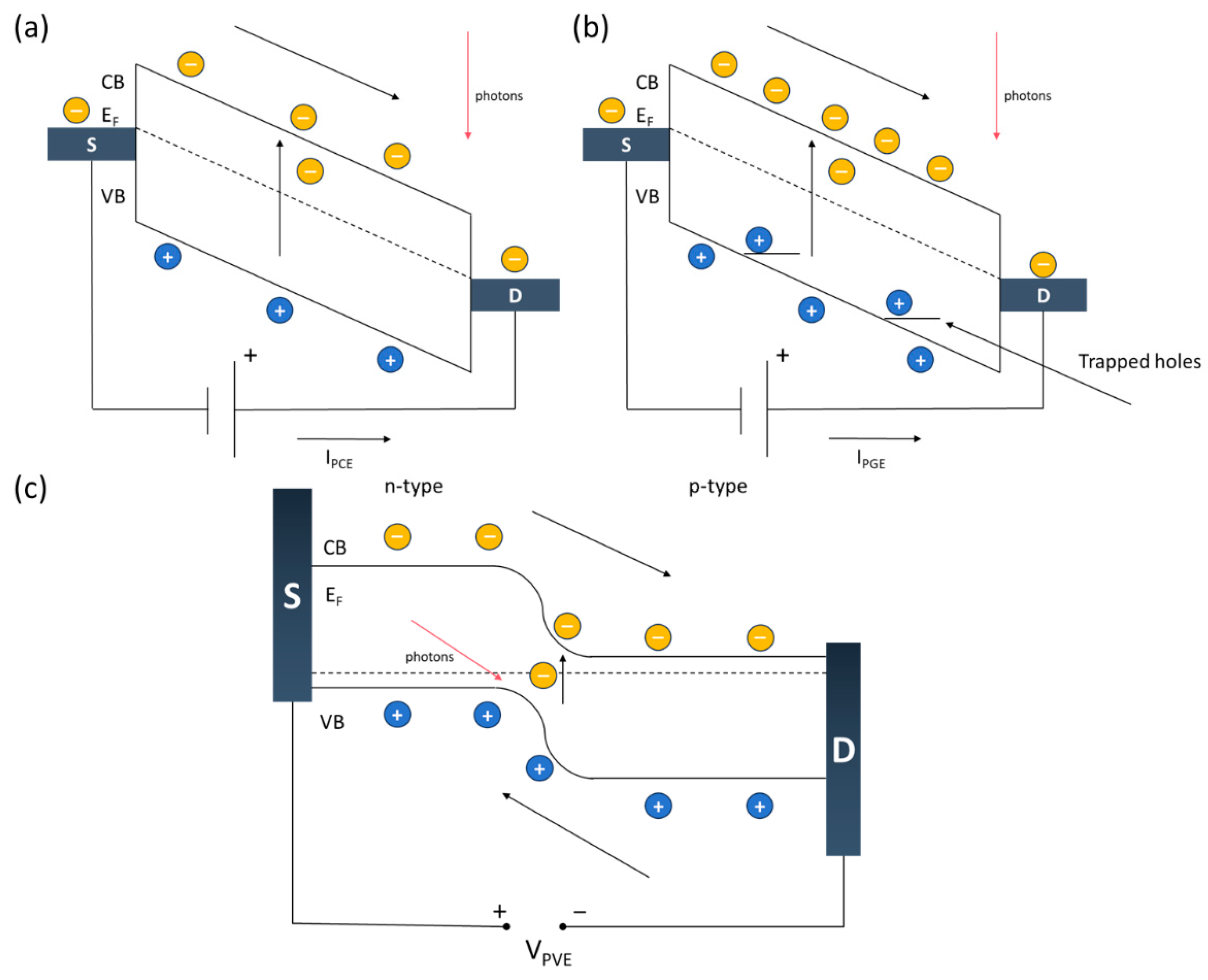
The photoconductivity effect (PCE) arises when a material absorbs photons with energy exceeding its bandgap, resulting in the excitation of electrons in the valence band (VB) to the induced band (CB), as shown in
Figure 1a. This leads to an increase in the generation of electron-hole (e–h) pairs and the concentration of free carriers, thereby enhancing the conductivity of the semiconductor. The change in conductivity is given by Δσ = ∆n·e·μ (where ∆n represents the change in the free carrier density, e is the unit charge, and μ is the carrier mobility of the channel parent layer). Even in the absence of light, the application of an external bias voltage can generate a current (I
dark). When irradiated by light, ∆σ can be converted to photocurrent I
ph by an external bias, which is given by I
ph = ∆·V·A (where V is the external bias voltage and A is the area of the illuminated region) [
21,
22].
The photogating effect (PGE) can be considered to be a specific case of the photoconductive effect (PCE), which also requires external bias [
22]. The photoconductivity gain (G) is defined as the ratio of the number of emitted charge carriers to the number of corresponding incident photons and is given by G = τ
life/τ
tran (where τ
life is the carrier lifetime and τ
tran is the carrier transition time between the electrodes) [
23] and I
ph is proportional to the gain. By increasing the probability of charge trapping and constructing heterostructures by creating defect traps, a longer τ lifetime and increased G can be achieved [
24,
25]. As is shown in
Figure 1b, the hole-trapping charge-trapping state can act as a local floating gate in n-type semiconductors, providing an effective method for modulating channel conductivity [
26], and vice versa for p-type semiconductors.
In phototransistors based on the photovoltaic effect (PVE), the built-in electric field in the p-n junction or Schottky junction separates the photogenerated e-h pairs, as shown in
Figure 1c. In the case of an open circuit, the electron-hole (e-h) pair accumulates on the relative terminal of the device, resulting in a reverse, low dark current, and excellent quantum efficiency [
23,
27] open-circuit voltage (V
OC). If the circuit is connected, a short-circuit current (I
SC) is generated. Unlike the PCE, in PVE, an external bias is not necessary to generate current, but it can help [
11] when the external bias is zero or reversed.
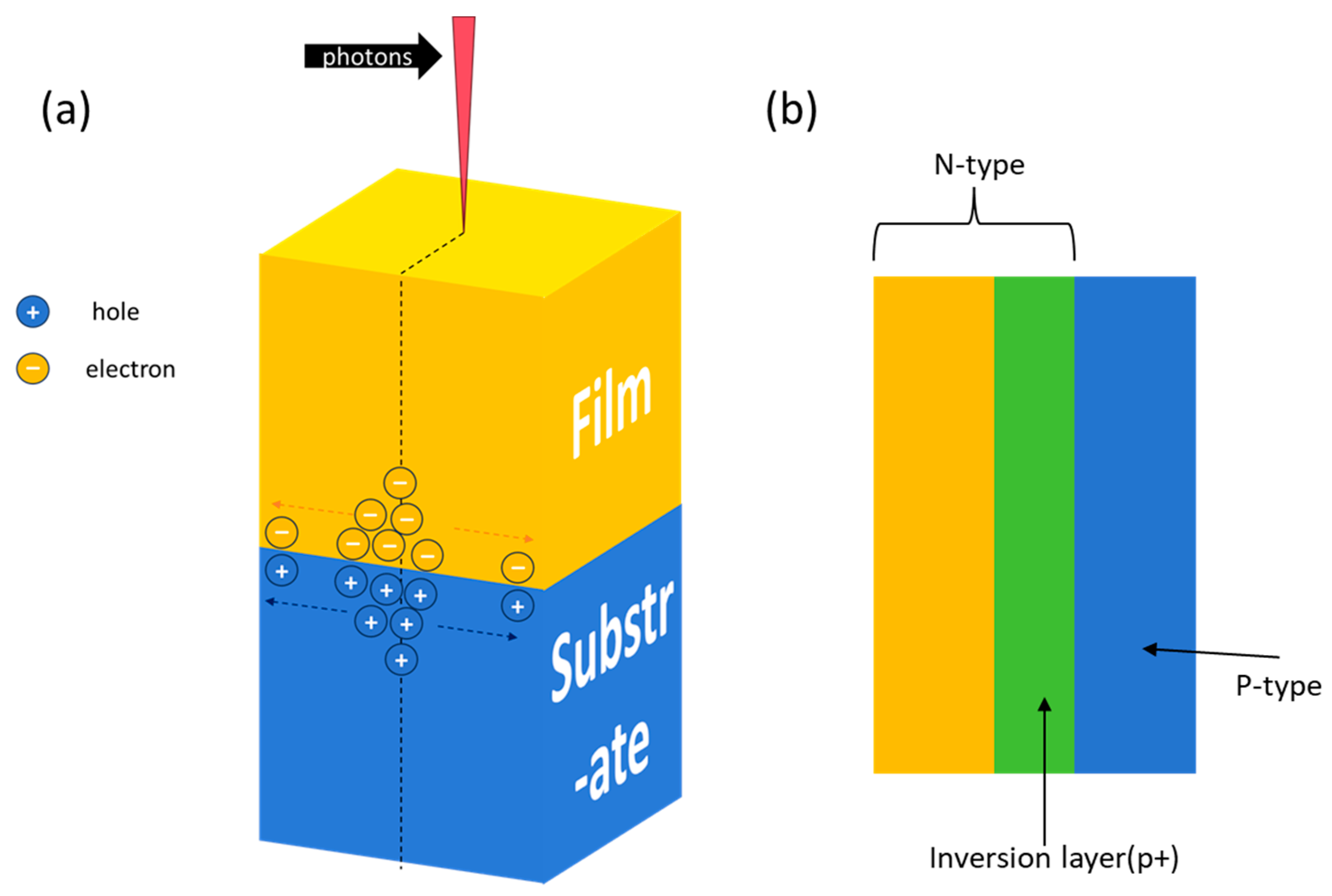
At the same time, Schottky and Walmark discovered the lateral photovoltaic effect (LPE) in p-n junctions [
28]. In the LPE, when one side of the p-n junction is illuminated by a spot, the optically excited electron-hole pairs will be separated up and down by the built-in electric field, and the carriers diffuse laterally. This mechanism can be explained using the model shown in
Figure 2a. The photogenerated electrons enter the n-type semiconductor and the photogenerated holes enter the p-type semiconductor. These generated carriers then diffuse laterally from the spot to balance the electric field along the layer. A typical structure of p-n junctions [
29,
30,
31] that can produce this effect is shown in
Figure 2b.
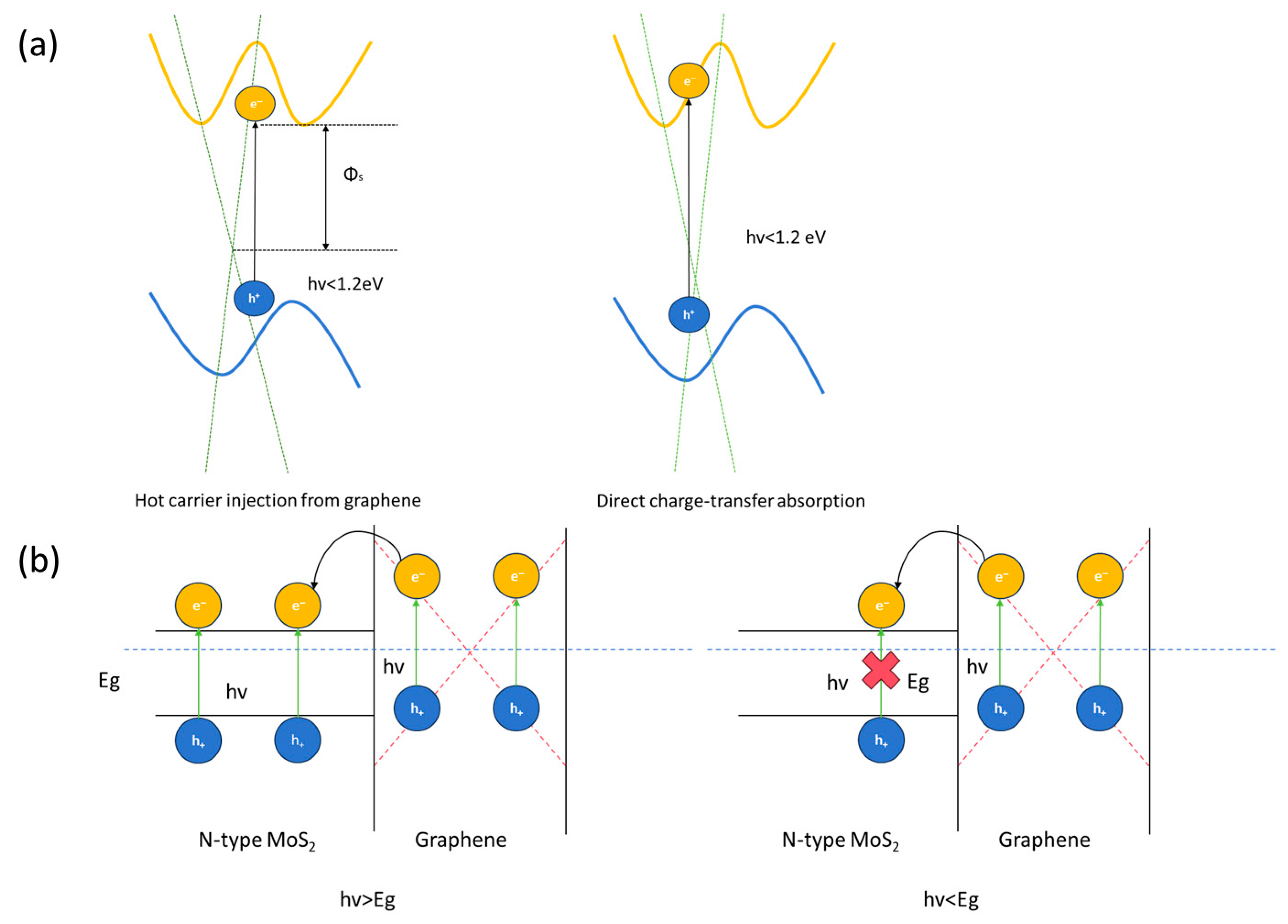
Specific to the device, the mechanism of photogenerated carriers in the graphene/MoS
2 heterojunction in this study is that the photons in the MoS
2 layer are absorbed by the graphene layer and the hot carriers are then transferred from graphene to MoS
2, resulting in the generation of a photocurrent below the bandgap in the graphene/MoS
2 heterojunction. The carrier excitation mechanism is shown in
Figure 3a, and the energy-band analysis is shown in
Figure 3b.
In the phototransistors based on the graphene/MoS2 heterojunction, the gate voltage effectively electrostatically modulates the channel carrier concentration through the field effect mechanism. When the gate voltage (Vgs) is applied, the electric field generated in the vertical direction will act on both graphene and MoS2. When Vgs > 0, the electric field attracts electrons to accumulate in the channel. On the one hand, the Fermi level of graphene is tuned to the conduction band to increase its electron concentration; on the other hand, the n-type characteristics of the MoS2 layer are significantly enhanced, and the background electron density is increased. On the contrary, when Vgs < 0, the electric field depletes the channel electrons, induces graphene hole conduction, and suppresses the electron concentration of MoS2. This synergistic regulation directly determines the dark conductivity of the device, and affects the separation and transport efficiency of photogenerated electron-hole pairs by changing the band bending and built-in electric field at the heterojunction interface.
4. Results and Discussion
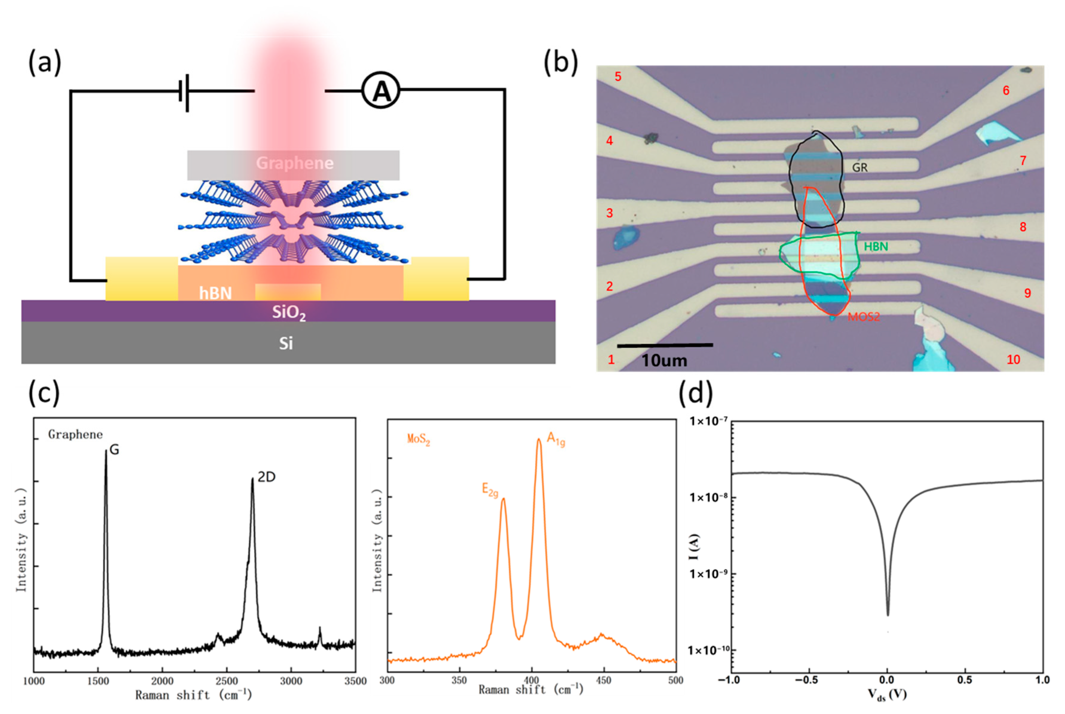
Figure 4a shows a diagram of the device structure. The MoS
2 film of the heterojunction was stacked on top of a boron nitride gate sheet, with two metal contacts on the heterojunction film. Boron nitride serves as an insulator for the gate. A gate bias was applied to the heavily doped silicon back gate, and the insulating layer material was silicon dioxide. During the optical measurement process, the beam was incident from the top of the device.
Figure 4b shows an optical microscope photograph of the graphene/MoS
2 heterostructure device. The black line indicates the outline of the graphene film stacked on the boron nitride gate, the red line indicates the outline of the MoS
2 film forming a heterojunction with graphene, and the green area indicates the position of the boron nitride sheet. According to
Figure 4b, electrode No. 2 is the gate, electrode No. 1 is the drain, electrode No. 4 is used as the source in the variable gate voltage test, and electrode No. 8 is used as the source in the variable light intensity test.
Figure S1 shows the results of estimating the thickness of the graphene/MoS
2 film by atomic force microscopy (AFM).
Figure S1a shows the thickness estimation result of MoS
2, which was measured to be approximately 2.2 nm, and the single layer thickness is about 0.7 nm, so MoS
2 comprises about 3 layers.
Figure S1b is the result of the graphene thickness estimation, which was measured to be approximately 3.0 nm, and the single-layer thickness is approximately 0.34 nm, so the graphene comprises about 8 layers.
Figure S2 shows the results of estimating the thickness of the boron nitride by atomic force microscopy (AFM). The thickness of the boron nitride was measured to be approximately 8.0 nm. The Raman spectra of the graphene/MoS
2 heterostructures are shown in
Figure 4c, and the characteristic peaks of MoS
2 and graphene are clearly visible.
Figure 4d shows the logarithmic I–V curve of the device in the absence of light conditions, which shows that the transport performance of the device is stable. The electrode used in this device is a gold electrode, which forms a Schottky contact with multilayer MoS
2, and the energy band structure is a rectified Schottky junction [
32]. Since the work function of gold (Au) (~5.1 eV) is higher than that of MoS
2, the two contact to form a Schottky junction, and there is a Schottky barrier of 0.1–0.4 eV [
32,
33], which explains the nonlinear characteristics of the I–V curve at low bias.
The light irradiation area is shown in the
Figure S3, and the irradiation diameter is 35.6 um.
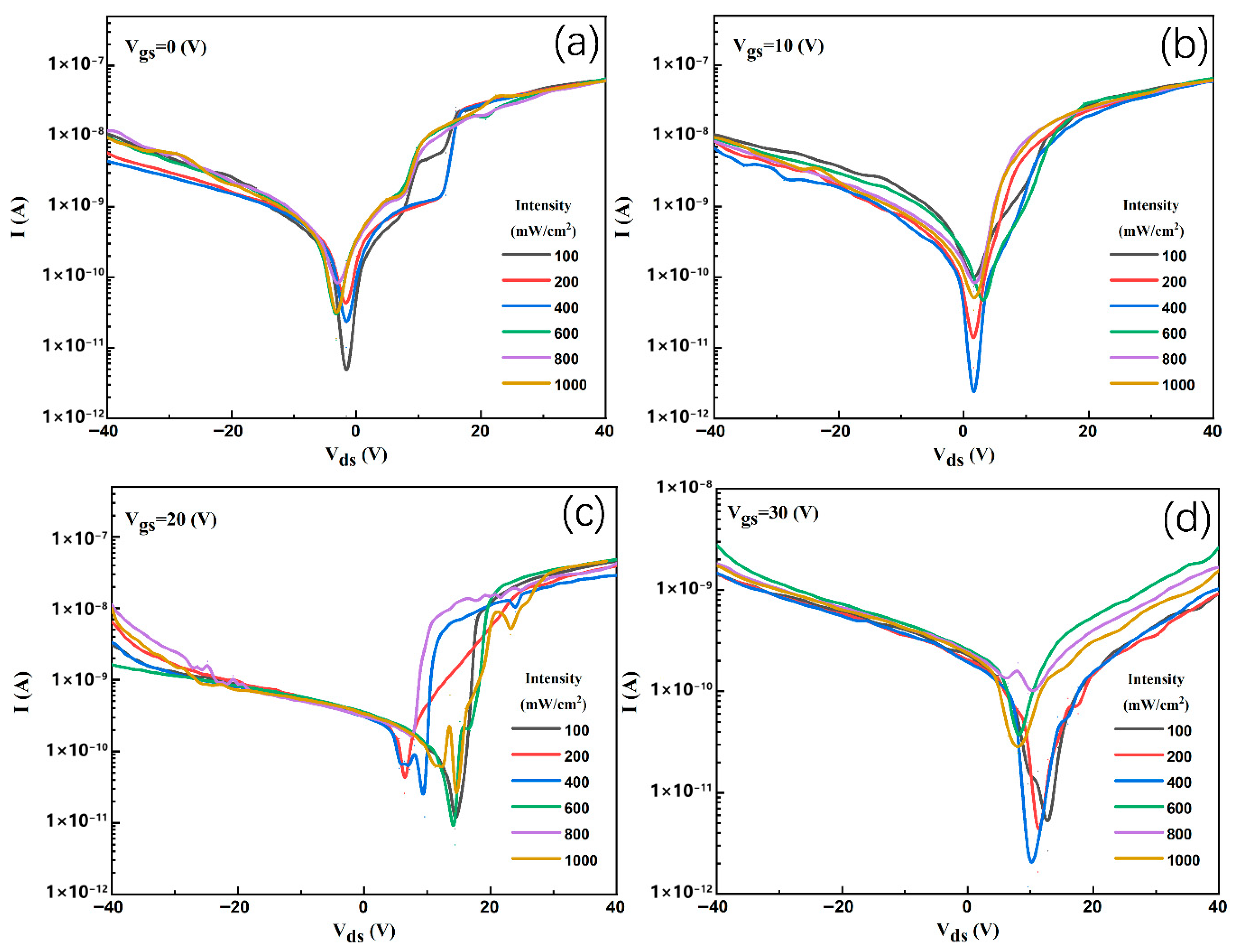
Figure 5 shows the variable light intensity transmission characteristics of the device under different gate voltages at room temperature.
Figure 5a–d show the photoelectric volt-ampere characteristic curves at gate voltages of 0, 10 V, 20 V, and 30 V, respectively. The curves of different colors represent the source-drain current measured under different light intensities. As is shown in the figure, as V
gs increased from 0 to 30 V, the dark current (valley bottom near V
ds = 0) gradually increased. When V
gs = 0 V, the dark current was ~10
−11 A, and when V
gs = 30 V, the dark current was close to 10
−10 A. Because the gate voltage regulates the carrier concentration of the graphene/MoS
2 heterojunction channel, more carriers were injected into the positive gate voltage, which improved the dark-state conductivity. Simultaneously, the photocurrent (∆I = I
light − I
dark, strong light intensity; for example, the difference between 1000 mW/cm
2 and the dark current) increases relative to the dark current. For example, when the light intensity is 1000 mW/cm
2 in
Figure 5b, the nearby photocurrent is approximately 10
−8~10
−9 A, and the difference in the photocurrent under weak light (100 mW/cm
2) is one order of magnitude smaller than that in the dark current. Under the same V
gs, the higher the light intensity, the more significant the current rise in the positive/negative bias region (the greater the deviation between the curve and the dark state). When V
gs = 10 V in
Figure 5b, the current curve of 1000 mW/cm
2 light intensity is significantly higher than that at 100 mW/cm
2, indicating that the dominant current of photogenerated carriers is enhanced, the density of photogenerated carriers is higher under strong light, and the modulation of the channel conductance is more significant. The photoelectric switching ratio (S = I
max, light/I
dark, I
max, light is the maximum value of strong light and strong current) is 100. By analyzing S, it can be concluded that, under a positive gate voltage (as shown in
Figure 5d), the ‘on state’ of the photocurrent is more obvious (the difference between the strong light and the dark state current is larger). This is because the gate voltage pre-modulates the carriers, and the photo-generated and gate-controlled carriers synergistically enhance the photoelectric response. According to the calculation, the responsivity of the device is 0.5023 mA/W. Although it is not as high as dozens of A/W of some high-performance heterojunctions (such as MoS
2/Si), the responsivity of 0.5023 mA/W is already competitive under the conditions of no complex process, no refrigeration, and normal temperature operation, which is especially suitable for low-power, flexible, and integrated optoelectronic systems.
Compared with state-of-the-art photodetectors based on similar van der Waals heterostructures, our graphene/MoS
2 phototransistor exhibits a distinct advantage in the gate-tunable and dynamically programmable photoresponse, despite its moderate responsivity (~5 × 10
−4 A/W). For instance, vertically stacked graphene/MoS
2/graphene devices have demonstrated remarkably high responsivity (exceeding 400 A/W) and broadband detection from visible to infrared wavelengths [
34], while sophisticated p-n diodes employing 2D metallic contacts (e.g., WTe
2) have achieved high responsivity (~47 A/W) and a gate-switchable bipolar photoresponse [
35]. In contrast, the novelty of our work lies not in competing for the highest absolute sensitivity, but in leveraging the back-gate terminal to actively and continuously modulate the device’s operating point. As is shown in
Figure 5 and
Figure 6, key figures of merit such as the dark current, photocurrent, and photocurrent-to-dark-current ratio can be precisely engineered by the gate voltage (V
gs). This “electrically programmable” functionality enables a single device to adapt its responsivity and noise floor for different lighting conditions—a feature not emphasized in the aforementioned high-performance but static-operation devices [
34,
35]. Therefore, our device serves as a versatile platform for tunable optoelectronics and provides fundamental insights into the synergistic interplay between gate-induced and photo-generated carriers in 2D heterojunctions.
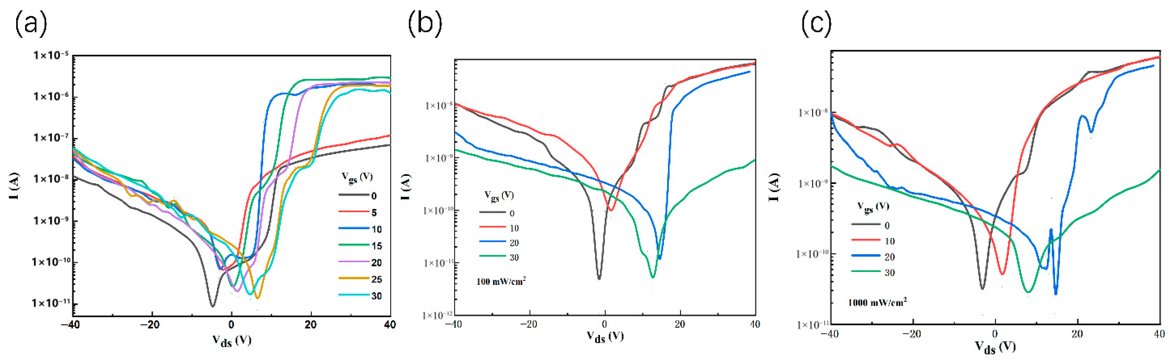
Figure 6 shows the variable gate voltage transmission characteristics of the device at room temperature under different incident light intensities.
Figure 6a,
Figure 6b and
Figure 6c show the source-drain current corresponding to different gate voltages when there is no incident light, when the incident light intensity is 100 mW/cm
2, and when the incident light intensity is 1000 mW/cm
2, respectively. By comparing
Figure 6b,c, it can be seen that under the same gate voltage, when the light intensity increased from 100 mW/cm
2 to 1000 mW/cm
2, the source-drain current increased significantly. For example, when V
gs = 20 V and V
ds = 20 V, the current in
Figure 6b is approximately 10
−9, whereas that in
Figure 6c is approximately 10
−8 A. This indicates that the number of photogenerated carriers increases with the increase in light intensity, which significantly improves the source-drain current of the device. The increase in light intensity also increases the slope of the volt-ampere curve, which means that the conductivity of the device increases. This is because the photogenerated carriers participated in conduction and enhanced the conductivity of the device.
As is shown in
Figure 6a (dark state), as V
gs increases from 0 V to 30 V, the change trend in the source-drain current is more complicated. When V
ds is positive, with an increase in V
gs, the current first decreases and then increases, which may be due to the regulation of the carriers in the heterojunction channel by the gate voltage. The gate voltage can change the carrier concentration and mobility in the channel, thereby affecting the current.
In
Figure 6a, when V
gs rises to 20 V, the dark current of the device does not approach zero, which is consistent with the working mechanism of the field effect transistor. The physical essence is the effective regulation of the gate voltage on the Fermi level of the channel: when the positive gate voltage is applied, the vertical electric field penetrates the gate dielectric, so that the energy band of the graphene/MoS
2 heterojunction channel moves down as a whole, and the Fermi level moves accordingly. For n-type MoS
2, the Fermi level is close to the bottom of the conduction band. For graphene, its Fermi level goes up through the Dirac point and enters the electron doping region. This band modulation process electrostatically induces a high concentration of electron carriers in the channel, which significantly enhances the conductivity of the channel. Therefore, even in the absence of illumination, these gate-induced carriers can form a considerable dark current driven by the source-drain voltage V
ds, and their density increases monotonically with the increase in V
gs. This behavior clearly confirms that the gate has an effective carrier accumulation ability for the heterojunction channel, and the device works in the n-type enhancement mode.
Figure 6b,c show that the gate voltage also has a significant regulatory effect on the current under light conditions. At higher light intensities, as shown in
Figure 6c, the regulation of the gate voltage on the current is more obvious. This is because the interaction between the photogenerated carriers and gate-voltage-regulated carriers makes the current more sensitive to the gate voltage response.
As is shown in
Figure 6c, when V
gs = 30 V, the maximum photocurrent can be obtained at a high light intensity compared with other gate voltage values, indicating that the synergistic effect of light intensity and gate voltage at this time achieved good results. This is because there is a synergistic effect between the light intensity and the gate voltage, which affects the current characteristics of the device. A higher light intensity provides more photogenerated carriers, and an appropriate gate voltage can optimize the transport of these photogenerated carriers in the channel, thereby significantly improving the photoelectric performance of the device.
In
Figure 6, the increase in photocurrent relative to the dark current is not significant. The physical reason is that the device works in a photoconductive mode without internal gain. The calculated photoconductive gain (G) is about 0.001, indicating that the photon-electron conversion efficiency is low. At the same time, under a high positive gate voltage, the gate-induced background carrier concentration is extremely high, so that the contribution of photogenerated carriers is diluted in terms of relative changes. In addition, the Schottky barrier at the metal–semiconductor interface may limit the efficient collection of carriers. Compared with those devices that use trap-assisted or avalanche multiplication effects to achieve a high gain (G >> 1) [
19,
20], although this device does not have an advantage in terms of absolute sensitivity, it has a simple structure, stable response, and easy gate control. It is still valuable in application scenarios where sensitivity, speed, and integration need to be weighed (such as simple photoelectric sensors or tunable photoelectric devices).
In order to further understand the photoresponse mechanism of the device, we analyzed the scaling relationship between the photocurrent (∆I = I
light − I
dark) and the incident light intensity (P), which usually follows the power-law dependence of ∆I ∝ P
μ. As is shown in
Figure 5 and
Figure 6, the ∆I of the device increases monotonically with the increase in P. However, when the light intensity increases from 100 mW/cm
2 to 1000 mW/cm
2, the growth rate of ∆I is less than one order of magnitude, indicating that it exhibits a sub-linear response, and the fitted index β is < 1. This behavior is more common in photodetectors based on transition metal chalcogenides, which is mainly attributed to the trap-assisted recombination dominated by internal defects and interface states at higher photogenerated carrier concentrations. At a low light intensity, the trap state is not saturated, and the carrier collection efficiency is high. At a high light intensity, the sharply increasing recombination process nonlinearly weakens the photocurrent gain, resulting in a decrease in the β value. This analysis confirms that although the device has good photoelectric responsiveness, its final performance is limited by the quality of the MoS
2 layer and the heterojunction interface.
In this study, the graphene/MoS
2 heterojunction phototransistor addresses several fundamental limitations inherent to pristine graphene-based field-effect transistors (GFETs). While GFETs exhibit exceptional carrier mobility and high-frequency potential, their zero-bandgap nature leads to poor current switching ratios and high off-state (dark) currents, which are major obstacles for applications in digital electronics and high-sensitivity photodetection [
36]. In contrast, by integrating MoS
2, this device introduces a substantial effective bandgap, enabling a significantly lower and gate-tunable dark current (as low as ~10
−11 A at V
gs = 0 V,
Figure 5a). This effectively mitigates the high noise floor typically associated with graphene-only photodetectors. Furthermore, the heterojunction facilitates efficient photoexcitation and carrier separation within the MoS
2 layer, generating a well-defined photocurrent. Most notably, the device retains the excellent gate controllability of graphene, allowing for continuous and dynamic modulation of both the dark current and photoresponse through the back-gate voltage (V
gs), as comprehensively detailed in
Figure 5 and
Figure 6. This gate-programmable functionality allows the device’s operating point and effective sensitivity to be tailored electrically—a feature that not only circumvents the static performance limitations of classic GFETs [
36] but also provides a versatile platform for adaptive optoelectronics. Compared with conventional monolayer MoS
2 field-effect transistors (FETs) documented in the literature, the graphene/MoS
2 heterojunction phototransistor presented in this paper demonstrates enhanced functionality alongside mitigated limitations. While early single-layer MoS
2 FETs achieved high on/off ratios (~10
8) and a low subthreshold swing (~74 mV/dec), they often suffered from persistent issues such as significant contact resistance, hysteresis induced by interface traps, and performance sensitivity to ambient conditions [
37]. In contrast, this device leverages the graphene/MoS
2 van der Waals heterostructure to synergistically combine the high carrier mobility and superior gate tunability of graphene with the appropriate bandgap of MoS
2. As is evidenced by
Figure 5 and
Figure 6, the back-gate voltage (V
gs) enables continuous and dynamic modulation of key figures of merit over more than three orders of magnitude: the dark current can be tuned as low as ~10
−11 A, the photocurrent is effectively enhanced, and the photocurrent-to-dark-current ratio reaches up to 100. This “electrically programmable” photoresponse represents a significant advancement over static high-performance MoS
2-based photodetectors (e.g., MoS
2/Si junctions) [
19,
20], directly addressing challenges related to environmental stability and functional inflexibility inherent in many conventional MoS
2 devices [
37] Consequently, this paper not only reports on a high-performance heterojunction phototransistor but also highlights its unique potential for reconfigurable and adaptive optoelectronic sensing applications.