
Spin and Charge Transport in the X-ray Irradiated Quasi-2D Layered Compound: κ-(BEDT-TTF)2Cu[N(CN)2]Cl

1. Introduction
 , where
  denotes the angle from a in the (a,b) plane.
, where denotes the angle from a in the (a,b) plane.
denotes the angle from a in the (a,b) plane.
, where denotes the angle from a in the (a,b) plane.
 . The relation between interlayer hopping and resistivity (Section 3) is most important for the interpretation. Details of the method and the high frequency ESR results in non-irradiated κ-ET2-Cl and κ-ET2-Br were published in References [7,8]. Section 4 presents the experimental results. Irradiation has little effect on both interlayer coupling and intralayer spin relaxation at 250 K and we argue in Section 4.1 that the concentration of irradiation-induced defects is low. In Section 5 we discuss possible mechanisms for the qualitative changes in the electronic transport.
2. Experimental
from the a axis in the (a,b) plane. In this paper we present only the data from which the interlayer hopping rate is determined. The ESR spectra were taken at 111.2 GHz and 222.4 GHz in the BUTE ESR Laboratory [11]. ρ|| in-plane and  interplane resistivity data were measured on different crystals and with different irradiation doses but under the same conditions as used for ESR. The difficulty of contacting make absolute values of and in particular of ρ|| uncertain.
 2.1. Method of Measuring ![]()
by ESR is based on the assumption that spin and charge hopping rates are equal. We use the convention  , where 1/Tx is the spin cross relaxation rate due to hopping from one layer to the two adjacent layers. In κ-ET2-Cl
  and
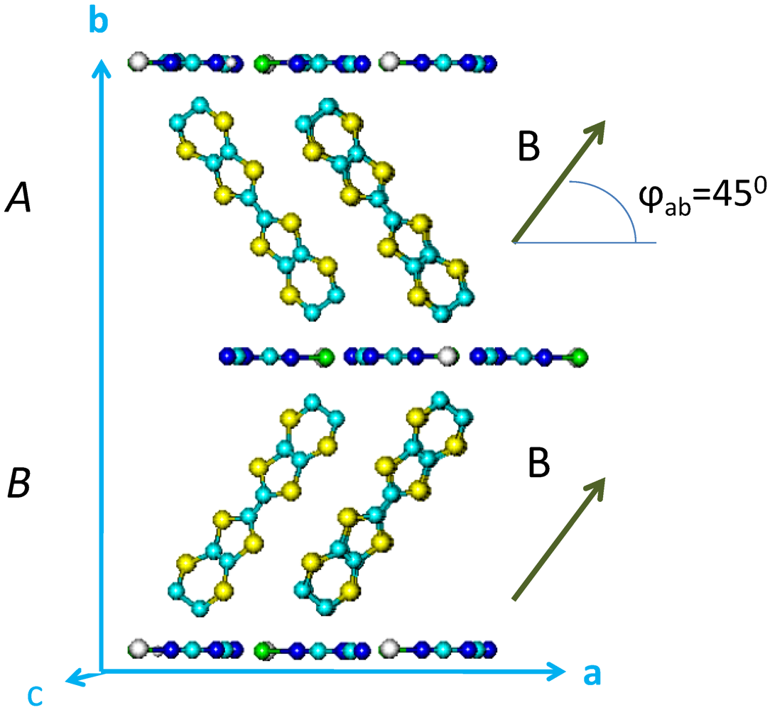
and  , the spin relaxation rates of conduction electrons due to processes intrinsic to layers A and B are long (i.e., in the ns range); consequently the ESR spectrum depends sensitively on interlayer hopping. can be measured by electron spin resonance (ESR) in materials like κ-ET2-Cl where chemically equivalent but structurally different layers (denoted by A and B in Figure 1) alternate [8]. If the A and B layers do not interact, the ESR spectrum is a superposition of two lines at the Larmor frequencies νA and νB. Since the g-factor tensors of A and B layers are differently oriented, the A and B lines are resolved in sufficiently high magnetic fields. In κ-ET2-Cl the splitting is largest in fields oriented along in the (a,b) plane while it is zero in the (a,c) plane and in the principal crystallographic directions. For a finite interaction between adjacent layers the ESR spectrum depends on the strength of the interlayer interaction, i.e., on the magnitude of :
 - (a)
![]() . The two lines are resolved; the lineshapes differ only slightly from the non interacting case.
. The two lines are resolved; the lineshapes differ only slightly from the non interacting case. - (b)
![]() . The spectrum has a complicated lineshape.
. The spectrum has a complicated lineshape. - (c)
![]() . A “motionally narrowed" line appears at the frequency
. A “motionally narrowed" line appears at the frequency ![]() . The linewidth depends on
. The linewidth depends on ![]() .
.


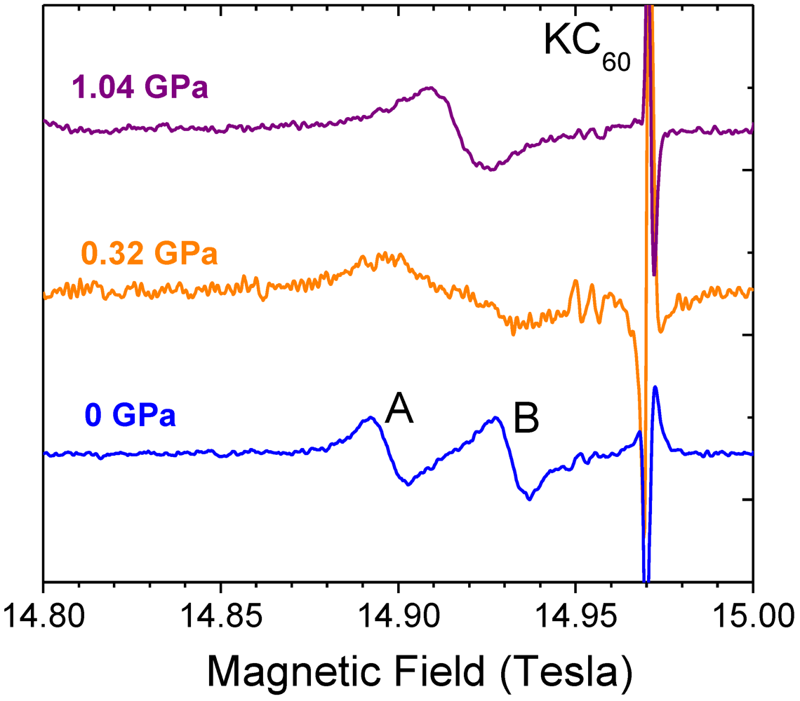
 was increased by applying pressure [7].. The spectra were measured at 420 GHz, T = 250 K and pressures of 0, 0.32 and 1.04 GPa. KC60 is an ESR reference.
. The spectra were measured at 420 GHz, T = 250 K and pressures of 0, 0.32 and 1.04 GPa. KC60 is an ESR reference.
was increased by applying pressure [7].. The spectra were measured at 420 GHz, T = 250 K and pressures of 0, 0.32 and 1.04 GPa. KC60 is an ESR reference.
. The spectra were measured at 420 GHz, T = 250 K and pressures of 0, 0.32 and 1.04 GPa. KC60 is an ESR reference. and
and  , the lineshapes are fitted to spectra calculated from two coupled Bloch equations. The electronic exchange between layers represented by an effective magnetic field is also included in the fit. In this paper all data were obtained by fitting ESR spectra recorded at two frequencies, 222.4 GHz and 111.2 GHz. gA and gB were also free parameters, they change little with temperature.
 3. Relation between Interlayer Hopping ![]() and Resistivity
and Resistivity ![]()
and are closely related [12]. The resistivity is proportional to the hopping time and inversely proportional to the density of available states, D. The electrical current j is given by 
 =
=  is the potential difference between adjacent layers due to the electric field
  . The relation is particularly simple if the electrons of molecular layers form a Fermi liquid. Then D = D(EF) is the density of states (DOS) per ET dimer for both spin directions of the metallic layers at the Fermi energy, EF. The perpendicular conductivity calculated from the hopping rate is
 the out-of-plane lattice constants. The significance of Equation (2) lies in the possibility to determine the DOS from measurements of the perpendicular resistivity and spin cross relaxation time without knowing details of the barrier between layers:
 and
and  is replaced by
  in Equation (3).
 for the Cl compound and the same for the Br compound within experimental accuracy. The conduction is quasi-two-dimensional: at 250 K electrons are confined to single layers for times several orders of magnitude longer than the momentum relaxation time. The density of states estimated from Equation (2) is about a factor of 5 larger than calculated from the band structure. Between 250 K and 50 K Tx increases rapidly with decreasing temperature in the Cl compound while it is about constant in the Br compound.
4. Interlayer Hopping Rate and Resistivity above the Metal Insulator Transition
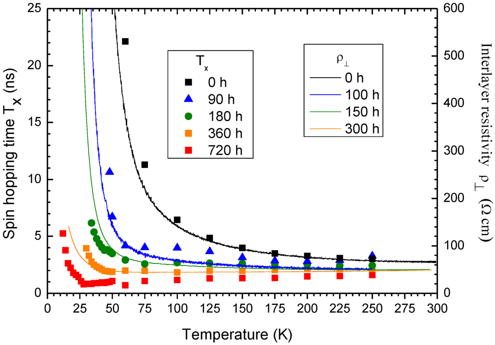
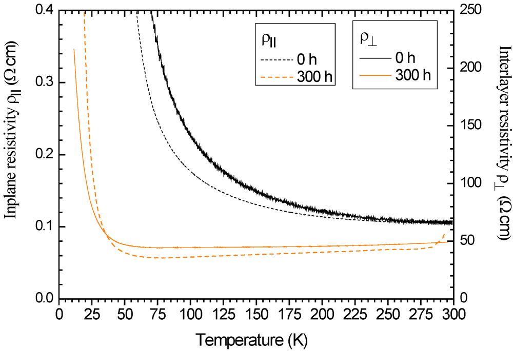
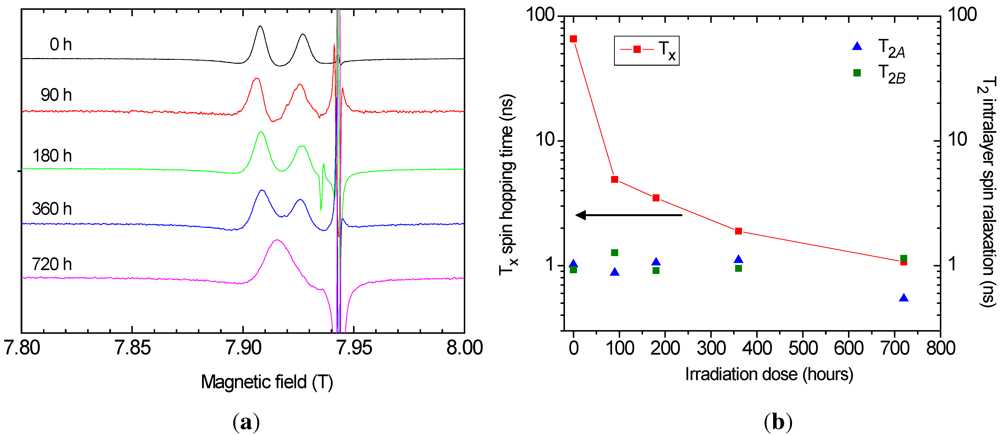
 and the perpendicular resistivity above the metal-insulator transition at various irradiation doses are summarized in Figure 3. The irradiation doses are in the same range in the two experiments. The scales of Tx and are chosen in the figure so that the experimental points of Tx and coincide at 250 K for the non-irradiated sample. Figure 4 displays the in-plane and interplane resistivities ρ|| and respectively of non-irradiated and 300 h irradiated samples. The resistivities in Figure 3 and Figure 4 are similar to the ones measured on a different crystal in Reference [6]. The resistivity
  in this work agrees reasonably well with the measurements of Reference [13]. smoothly increasing as the temperature is decreased. On the contrary, the 180 h and more irradiated samples have a metallic like behavior: Tx and decrease with decreasing temperature. In the irradiated samples the abrupt metal-insulator transition is qualitatively different from the smooth transition in the non-irradiated sample. Furthermore, irradiation shifts the transition to lower temperatures. and ρ|| have similar temperature and irradiation dependence. The ratio /ρ|| is about 600 independent of temperature for both the irradiated and non-irradiated samples. This ratio, even if uncertain, is typical for measurements in the literature.
 and interlayer resistivity
  in κ-ET2-Cl. Left scale: Tx after 0, 90, 180, 360 and 720 h of irradiation. Right scale: after 0, 100, 150 and 300 h of irradiation.
and interlayer resistivity in κ-ET2-Cl. Left scale: Tx after 0, 90, 180, 360 and 720 h of irradiation. Right scale: after 0, 100, 150 and 300 h of irradiation.
in κ-ET2-Cl. Left scale: Tx after 0, 90, 180, 360 and 720 h of irradiation. Right scale: after 0, 100, 150 and 300 h of irradiation.
and interlayer resistivity in κ-ET2-Cl. Left scale: Tx after 0, 90, 180, 360 and 720 h of irradiation. Right scale: after 0, 100, 150 and 300 h of irradiation.  in non-irradiated and 300 hours irradiated κ-ET2-Cl. ρ|| and were measured on different samples.
in non-irradiated and 300 hours irradiated κ-ET2-Cl. ρ|| and were measured on different samples.
in non-irradiated and 300 hours irradiated κ-ET2-Cl. ρ|| and were measured on different samples. 
4.1. Irradiation Dependence of ![]() and
and ![]() at 250 K
at 250 K

 and
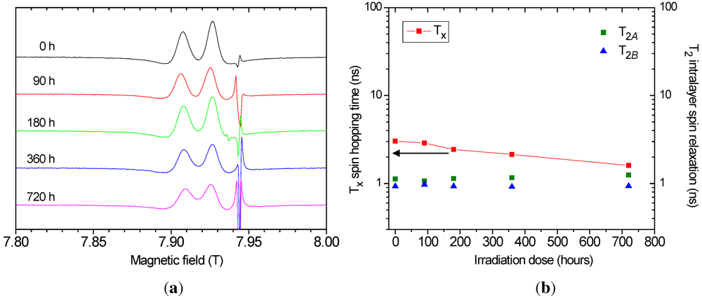
and  calculated from the spectra. Tx decreases by less then a factor of 2 for the largest dose while and are not changed significantly by the irradiation. in κ-ET2-Cl is about
  and electrons diffuse to long distances without hopping to adjacent layers. Although the irradiation increases somewhat , electrons remain confined to single molecular layers for long times. In addition,
  , the electronic spin relaxation time within the conducting ET layers, is independent of irradiation. Usually charged defects effectively increase the spin relaxation rate in conductors. The insensitivity of to irradiation and the relatively small decrease in Tx are in agreement with earlier findings [9] that the concentration of induced defects is small even under the largest dose. at 250 K.
at 250 K.
, the electronic spin relaxation time within the conducting ET layers, is independent of irradiation. Usually charged defects effectively increase the spin relaxation rate in conductors. The insensitivity of to irradiation and the relatively small decrease in Tx are in agreement with earlier findings [9] that the concentration of induced defects is small even under the largest dose. at 250 K.
at 250 K. at 50 K.
at 50 K.
at 50 K. 
4.2. Irradiation Dependence of ![]() and
and ![]() at 50 K
at 50 K
5 Discussion
- (1) The perpendicular resistivity
![]() is semiconducting-like in non-irradiated κ-ET2-Cl. Irradiation decreases
is semiconducting-like in non-irradiated κ-ET2-Cl. Irradiation decreases ![]() in the full temperature range, the decrease is non-linear with dose. At higher doses the resistivity is metallic, i.e., it increases linearly with temperature.
in the full temperature range, the decrease is non-linear with dose. At higher doses the resistivity is metallic, i.e., it increases linearly with temperature. - (2) The interlayer spin hopping time Tx and
![]() have the same temperature and irradiation dose dependence. The ratio
have the same temperature and irradiation dose dependence. The ratio ![]() is independent of temperature and irradiation dose.
is independent of temperature and irradiation dose. - (3) The resistivity anisotropy
![]() /ρ|| is typically between 100 and 1000. It is independent of temperature and irradiation dose.
/ρ|| is typically between 100 and 1000. It is independent of temperature and irradiation dose. - (4) The magnetic spin susceptibility is approximately temperature independent and does not change with irradiation [9].
- (5) Theintralayer spin relaxation time
![]() is independent of temperature and dose.
is independent of temperature and dose.
 and the perpendicular hopping time to resistivity ratio
  are both proportional to the density of states. Although κ-ET2-Cl is a strongly correlated system and at high temperatures there are no long lifetime quasi-particles, the independence of the susceptibility and the ratio indicate that the electronic structure is not strongly affected by the irradiation. The defect dose independence of , the relatively small decrease of Tx at 250 K with dose and earlier magnetic measurements [9] indicate that the defect concentration is small./ρ|| in materials where the perpendicular conductivity is incoherent. They showed that if the in-plane scattering time
  is much shorter than the interlayer hopping time
  , then the ratio /ρ|| is independent of . To understand the doping independence of /ρ|| one has to assume that irradiation introduces carriers with an increased but at the same time the parallel and perpendicular electronic overlap integrals remain unchanged. in κ-(BEDT-TTF)2 Cu(SCN)2, an organic conductor close to the Mott transition. The in-plane resistivity is assumed to be small and without any effect on . A defect-assisted interplane conductivity has also been proposed [15] to explain the metallic zero frequency interplane conductivity and the absence of a Drude peak in the optical conductivity in κ-ET2-Br. However, it is difficult to understand within this model the irradiation and temperature independence of the anisotropy between 50 and 250 K in κ-ET2-Cl. Due to difficulties in contacting and/or macroscopic sample imperfections, the current is usually inhomogeneous in strongly anisotropic conductors and in general the interlayer resistivity affects in-plane measurements. If ρ|| is very small, the contribution of might dominate the apparent in-plane resistivity. This would explain that and ρ|| have (apparently) the same temperature dependence both for the non-irradiated and irradiated crystal. However, this model does not explain why the anisotropy is independent of irradiation dose.
6 Conclusions
is unchanged in the range of irradiation doses where the resistivity changes from a semiconductor-like behavior to metallic. Since κ-ET2-Cl is a strongly correlated conductor close to the metal insulator and magnetic ordering transitions, the spin and charge hopping rates could have different temperature or doping dependence. The insensitivity of to doping and temperature makes this unlikely. The qualitative change of the temperature dependence of the resistivity with irradiation and the insensitivity of other quantities depending on the density of states poses a difficult problem, which is not yet satisfactorily resolved.Acknowledgements
References
- Williams, J.M.; Kini, A.M.; Wang, H.H.; Carlson, K.D.; Geiser, U.; Montgomery, L.K.; Pyrka, G.J.; Watkins, D.M.; Kommers, J.M.; Boryschuk, S.J.; Crouch, A.V.S.; Kwok, W.K.; Schirber, J.E.; Overmyer, D.L.; Jung, D.; Whangbo, M.H. From semiconductor semiconductor transition (42 K) to the highest-12.5 k organic superconductor, Kappa-(ET)2Cu[N(Cn)2]Cl. Inorg.Chem. 1990, 29, 3272–3274. [Google Scholar]
- Miyagawa, K.; Kawamoto, A.; Nakazawa, Y.; Kanoda, K. Antiferromagnetic Ordering and Spin Structure in the Organic Conductor, κ-(BEDT-TTF)2Cu[N(CN)2]Cl. Phys. Rev. Lett. 1995, 75, 1174–1177. [Google Scholar] [CrossRef]
- Welp, U.; Fleshler, S.; Kwok, W.K.; Crabtree, G.W.; Carlson, K.D.; Wang, H.H.; Geiser, U.; Williams, J.M.; Hitsman, V.M. Weak ferromagnetism in κ-(ET)2Cu[N(CN]2Cl, where (ET) is bis(ethylenedithio)tetrathiafulvalene. Phys. Rev. Lett. 1992, 69, 840–843. [Google Scholar] [CrossRef]
- Kawamoto, A.; Miyagawa, K.; Nakazawa, Y.; Kanoda, K. Electron correlation in the κ-phase family of BEDT-TTF compounds studied by 13C NMR, where BEDT-TTF is bis(ethylenedithio)tetrathiafulvalene. Phys. Rev. B 1995, 52, 15522–15533. [Google Scholar] [CrossRef]
- Antal, A.; Fehér, T.; Jánossy, A.; Tátrai-Szekeres, E.; Fülöp, F. Spin diffusion and magnetic eigenoscillations confined to single molecular layers in the organic conductors κ-(BEDT-TTF)2 Cu[N(CN)2]X (X=Cl, Br). Phys. Rev. Lett. 2009, 102. [Google Scholar] [CrossRef]
- Sasaki, T.; Oizumi, H.; Yoneyama, N.; Kobayashi, N.; Toyota, N. X-ray irradiation-induced carrier doping effects in organic dimer–mott insulators. J. Phys. Soc. Jpn. 2007, 76. [Google Scholar] [CrossRef]
- Antal, A.; Fehér, T.; Tátrai-Szekeres, E.; Fülöp, F.; Náfrádi, B.; Forró, L.; Jánossy, A. Pressure and temperature dependence of interlayer spin diffusion and electrical conductivity in the layered organic conductors κ-(BEDT-TTF)2 Cu[N(CN)2]X (X = Cl, Br). Phys. Rev. B 2011, 84. [Google Scholar] [CrossRef]
- Antal, A.; Fehér, T.; Náfrádi, B.; Gaál, R.; Forró, L.; Jánossy, A. Measurement of interlayer spin diffusion in the organic conductor κ-(BEDT-TTF)2 Cu[N(CN)2]X, X =Cl, Br. Phys. B Condens.Matter 2010, 405, 168–171. [Google Scholar]
- Yoneyama, N.; Furukawa, K.; Nakamura, T.; Sasaki, T.; Kobayashi, N. Magnetic properties of X-ray irradiated organic mott insulator κ-(BEDT-TTF)2 Cu[N(CN)2]Cl. J. Phys. Soc. Jpn. 2010, 79, 063706. [Google Scholar] [CrossRef]
- Sano, K.; Sasaki, T.; Yoneyama, N.; Kobayashi, N. Electron localization near the mott transition in the organic superconductor κ-(BEDT-TTF)2 Cu[N(CN)2]Br. Phys. Rev. Lett. 2010, 104. [Google Scholar] [CrossRef]
- Nagy, K.L.; Náfrádi, B.; Kushch, N.D.; Yagubskii, E.B.; Herdtweck, E.; Fehér, T.; Kiss, L.F.; Forró, L.; Jánossy, A. Multifrequency ESR in ET2MnCu[N(CN)2]4: A radical cation salt with quasi-two-dimensional magnetic layers in a three-dimensional polymeric structure. Phys. Rev. B 2009, 80. [Google Scholar] [CrossRef]
- Kumar, N.; Jayannavar, A.M. Temperature dependence of the c-axis resistivity of high-Tc layered oxides. Phys. Rev. B 1992, 45, 5001–5004. [Google Scholar] [CrossRef]
- Ito, H.; Ishiguro, T.; Kubota, M.; Saito, G. Metal-nonmetal transition and superconductivity localization in the two-dimensional conductor κ-(BEDT-TTF)2 Cu[N(CN)2]Cl under Pressure. J. Phys. Soc. Jpn. 1996, 65, 2987–2993. [Google Scholar] [CrossRef]
- Analytis, J.G.; Ardavan, A.; Blundell, S.J.; Owen, R.L.; Garman, E.F.; Jeynes, C.; Powell, B.J. Effect of irradiation-induced disorder on the conductivity and critical temperature of the organic superconductor κ-(BEDT-TTF)2 Cu(SCN)2. Phys. Rev. Lett. 2006, 96. [Google Scholar] [CrossRef]
- McGuire, J.J.; Rõom, T.; Pronin, A.; Timusk, T.; Schlueter, J.A.; Kelly, M.E.; Kini, A.M. Incoherent interplane conductivity of κ-(BEDT-TTF)2 Cu[N(CN)2]Br. Phys. Rev. B 2001, 64. [Google Scholar] [CrossRef]
© 2012 by the authors; licensee MDPI, Basel, Switzerland. This article is an open-access article distributed under the terms and conditions of the Creative Commons Attribution license (http://creativecommons.org/licenses/by/3.0/).
Share and Cite
Antal, Á.; Fehér, T.; Yoneyama, N.; Forró, L.; Sasaki, T.; Jánossy, A. Spin and Charge Transport in the X-ray Irradiated Quasi-2D Layered Compound: κ-(BEDT-TTF)2Cu[N(CN)2]Cl. Crystals 2012, 2, 579-589. https://doi.org/10.3390/cryst2020579
Antal Á, Fehér T, Yoneyama N, Forró L, Sasaki T, Jánossy A. Spin and Charge Transport in the X-ray Irradiated Quasi-2D Layered Compound: κ-(BEDT-TTF)2Cu[N(CN)2]Cl. Crystals. 2012; 2(2):579-589. https://doi.org/10.3390/cryst2020579
Chicago/Turabian StyleAntal, Ágnes, Titusz Fehér, Naoki Yoneyama, László Forró, Takahiko Sasaki, and András Jánossy. 2012. "Spin and Charge Transport in the X-ray Irradiated Quasi-2D Layered Compound: κ-(BEDT-TTF)2Cu[N(CN)2]Cl" Crystals 2, no. 2: 579-589. https://doi.org/10.3390/cryst2020579
APA StyleAntal, Á., Fehér, T., Yoneyama, N., Forró, L., Sasaki, T., & Jánossy, A. (2012). Spin and Charge Transport in the X-ray Irradiated Quasi-2D Layered Compound: κ-(BEDT-TTF)2Cu[N(CN)2]Cl. Crystals, 2(2), 579-589. https://doi.org/10.3390/cryst2020579