Gate-Induced Thermally Stimulated Current on the Ferroelectric-like Dielectric Properties of (BEDT-TTF)(TCNQ) Crystalline Field Effect Transistor

1. Introduction
2. Experimental Details
 ) was applied under 280 K and this poling bias was kept for 30 min. After the poling, the sample was cooled until about 90 K under the application of to freeze the gate-induced polarization. After was turned to 0 V, an electrical current from source electrode was measured under the constant sample heating rate of about 5 K/min. A thermally stimulated current was observed with the dissolution of initially frozen polarization.
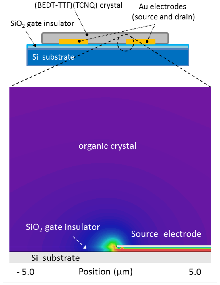
3. Results and Discussion

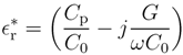
 . However in our case, it is impossible to transform Cp and G into the
  and
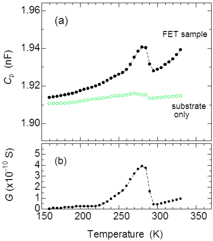
and  because an electric field is not uniform in the FET structure (see Figure 1 ). Although a parallel capacitor structure is generally used for conventional dielectric measurements, we had to observe a novel ferroelectric-like property which was observed in the channel region of FET structure [10] and had not been reported in bulk crystal. Both the observed Cp and G have a peak at around 280 K, and abruptly decrease at around 290 K. In our previous work [10], we suggested the existence of unknown ferroelectric-like transition by a displacement current measurement. In this work, the conventional impedance measurement also discovered this ferroelectric-like transition. However, compared to the typical ferroelectric transition, the observed temperature dependence of dielectric response is rather dispersive because the polarization in our sample is not uniform due to the non-uniformity of electric field in the crystal. ; (b) The TSCs observed in the substrate without (BEDT-TTF)(TCNQ) crystals.
; (b) The TSCs observed in the substrate without (BEDT-TTF)(TCNQ) crystals.
because an electric field is not uniform in the FET structure (see Figure 1 ). Although a parallel capacitor structure is generally used for conventional dielectric measurements, we had to observe a novel ferroelectric-like property which was observed in the channel region of FET structure [10] and had not been reported in bulk crystal. Both the observed Cp and G have a peak at around 280 K, and abruptly decrease at around 290 K. In our previous work [10], we suggested the existence of unknown ferroelectric-like transition by a displacement current measurement. In this work, the conventional impedance measurement also discovered this ferroelectric-like transition. However, compared to the typical ferroelectric transition, the observed temperature dependence of dielectric response is rather dispersive because the polarization in our sample is not uniform due to the non-uniformity of electric field in the crystal. ; (b) The TSCs observed in the substrate without (BEDT-TTF)(TCNQ) crystals.
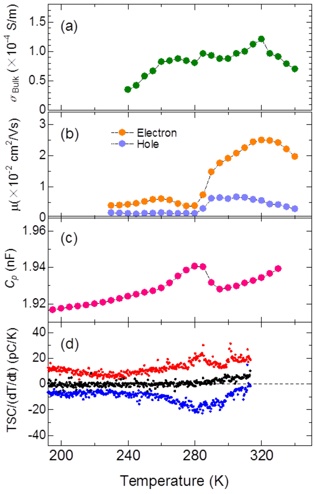
; (b) The TSCs observed in the substrate without (BEDT-TTF)(TCNQ) crystals.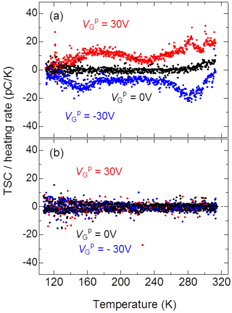 , positive TSC was observed. On the other hand, negative TSC was observed by application of negative . In addition, by application of zero , no TSC peak was observed. Only a minor increase of a TSC was observed above 290 K, which was also observed in a blank test which is described afterwards. The observed TSC under non-zero have a maximum at 285 K, and there are minor and broad peaks in 180–210 K. These minor and broad peaks do not belong to a pyroelectric current but correspond to detrapping of carriers because these peaks are not symmetric to the polarization of an applied . A thermal activation energy for electron and hole detrapping should be different. On the other hand, major TSC observed above 210 K belongs to a pyroelectric current because these peaks are symmetric to the polarization, and the TSC corresponds to the dielectric response and Q − V hysteresis observed in our previous work [10]. The Q − V hysteresis, divergent increase of dielectric constant and loss are a part of the feature of the ferroelectricity. Therefore, we concluded that the observed TSC corresponded to the dissolution of the ferroelectric-like polarization. and its polarity. In addition, the observed weak TSC decreases after the several thermal cycles. A possible origin of the weak TSC in the blank test is surface moisture or mobile alkali ion naturally diffused into the SiO2 layer. However, thick pre-fabricated SiO2 layer to protect the Si wafer from the alkali ion pollution is completely removed in the sample preparation procedure. Moreover, a contribution of alkali ion cannot decrease after several thermal cycles because alkali ion diffused in Si cannot vaporize in this experimental condition. Therefore, we conclude that the origin of the small TSC observed in the blank test is residual surface moisture at the substrate surface. Incidentally, the existence of ferroelectric phase of H2O is proposed at around 60 K [20]. However, this phase cannot affect our results. dependence of the observed TSCs; (b) Temperature and dependence of the remnant polarization charge. The values for the remnant polarization charge at the lowest temperature (Qini) was taken rather arbitrarily to let the remnant polarization charge be proportional to because it was difficult to determine the absolute value of Qini due to the non-uniform electric field.
dependence of the observed TSCs; (b) Temperature and dependence of the remnant polarization charge. The values for the remnant polarization charge at the lowest temperature (Qini) was taken rather arbitrarily to let the remnant polarization charge be proportional to because it was difficult to determine the absolute value of Qini due to the non-uniform electric field.
, positive TSC was observed. On the other hand, negative TSC was observed by application of negative . In addition, by application of zero , no TSC peak was observed. Only a minor increase of a TSC was observed above 290 K, which was also observed in a blank test which is described afterwards. The observed TSC under non-zero have a maximum at 285 K, and there are minor and broad peaks in 180–210 K. These minor and broad peaks do not belong to a pyroelectric current but correspond to detrapping of carriers because these peaks are not symmetric to the polarization of an applied . A thermal activation energy for electron and hole detrapping should be different. On the other hand, major TSC observed above 210 K belongs to a pyroelectric current because these peaks are symmetric to the polarization, and the TSC corresponds to the dielectric response and Q − V hysteresis observed in our previous work [10]. The Q − V hysteresis, divergent increase of dielectric constant and loss are a part of the feature of the ferroelectricity. Therefore, we concluded that the observed TSC corresponded to the dissolution of the ferroelectric-like polarization. and its polarity. In addition, the observed weak TSC decreases after the several thermal cycles. A possible origin of the weak TSC in the blank test is surface moisture or mobile alkali ion naturally diffused into the SiO2 layer. However, thick pre-fabricated SiO2 layer to protect the Si wafer from the alkali ion pollution is completely removed in the sample preparation procedure. Moreover, a contribution of alkali ion cannot decrease after several thermal cycles because alkali ion diffused in Si cannot vaporize in this experimental condition. Therefore, we conclude that the origin of the small TSC observed in the blank test is residual surface moisture at the substrate surface. Incidentally, the existence of ferroelectric phase of H2O is proposed at around 60 K [20]. However, this phase cannot affect our results. dependence of the observed TSCs; (b) Temperature and dependence of the remnant polarization charge. The values for the remnant polarization charge at the lowest temperature (Qini) was taken rather arbitrarily to let the remnant polarization charge be proportional to because it was difficult to determine the absolute value of Qini due to the non-uniform electric field.
dependence of the observed TSCs; (b) Temperature and dependence of the remnant polarization charge. The values for the remnant polarization charge at the lowest temperature (Qini) was taken rather arbitrarily to let the remnant polarization charge be proportional to because it was difficult to determine the absolute value of Qini due to the non-uniform electric field. 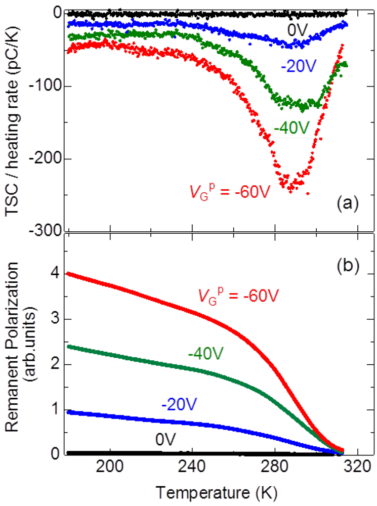 dependence of the observed TSCs. These TSCs increase with increasing because induced average polarization increase with increasing . However, the TSC peak temperature shows little dependence on the . In this temperature region, the observed TSC is expected to mainly consist of the pyroelectric current because the temperature range is higher than that of which the detrapping from the carrier traps are observed. On this basis, we integrated the observed TSCs. The relation between the polarization and observed TSC is written as


 ) is constant, one can obtain the pyroelectric coefficient. Then, Pr was calculated as an integration of the pyroelectric current i(T).
 dependence of the remnant polarization charge (Qr). Although the Qini is difficult to determine, because of the non-uniform electric field in the crystal, we determined the Qini for each on the assumption that the initially induced Qr is proportional to the . Figure 4 (b) indicates that Qr gradually decrease with increasing temperature until 260 K, and begin to decrease steeply at around 280–290 K. A little Qr remains at 320 K. These observed temperature dependence well corresponds to the temperature dependence of the Cp as shown in Figure 2 (a). Temperature dependence of Cp and previously observed hysteresis [10] had suggested the existence of ferroelectric phase transition, which is now supported by the additional evidence in this work.
4. Conclusions
and has a peak at around 285 K was assigned as a pyroelectric current derived from the spontaneous polarization of ferroelectricity. By integrating the pyroelectric current, temperature dependence of the remnant polarization charge was exhibited and the existence of the ferroelectric phase transition at 285 K was clearly demonstrated. With the calculated distribution of an electric field and obvious relationship of the field effect mobility and ferroelectric behavior, we have concluded that the observed novel phenomena is brought about at around the interface of organic crystal and substrate. Although the phenomena has not fully been elucidated yet, we temporarily concluded that the phase transition occurred between dimer Mott insulator and charge ordered phase. Acknowledgments
References
- Yamamoto, K.; Kowalska, A.A.; Yakushi, K. Direct observation of ferroelectric domains created by Wigner crystallization of electrons in α-[bis(ethylenedithio)tetrathiafulvalene]2I3. Appl. Phys. Lett. 2010, 96 122901-1-122901-3., 122901–1. [Google Scholar] [CrossRef]
- Yamamoto, K.; Kowalska, A.A.; Nakano, C.; Yakushi, K. Inhomogeneous ferroelectric polarization in α '-(BEDT-TTF)2IBr2 revealed by second-harmonic generation microscopy. Physica B 2010, 405, S363–S364. [Google Scholar] [CrossRef]
- Kowalska, A.A.; Yamamoto, K.; Nakano, C.; Yakushi, K. Ferroelectric Polarization in α-(ET)2I2Br Studied by Second -Harmonic Generation Microscopy. J. Phys. 2008, 132 012006-1-012006-5, 012006–1. [Google Scholar]
- Yamamoto, K.; Iwai, S.; Boyko, S.; Kashiwazaki, A.; Hiramatsu, F.; Okabe, C.; Nishi, N.; Yakushi, K. Strong Optical Nonlinearity and its Ultrafast Response Associated with Electron Ferroelectricity in an Organic Conductor. J. Phys. Soc. Jpn. 2008, 77 074709-1-074709-6., 074709–1. [Google Scholar] [CrossRef]
- Abdel-Jawad, M.; Terasaki, I.; Sasaki, T.; Yoneyama, N.; Kobayashi, N.; Uesu, Y.; Hotta, C. Anomalous dielectric response in the dimer Mott insulator κ-(BEDT-TTF)2Cu2(CN)3. Phys. Rev. B 2010, 82. [Google Scholar] [CrossRef]
- Niizeki, S.; Yoshikane, F.; Kohno, K.; Takahashi, K.; Mori, H.; Bando, Y.; Kawamoto, T.; Mori, T. Dielectric Response and Electric-Field-Induced Metastable State in an Organic Conductor β-(meso-DMBEDT-TTF)2PF6. J. Phys. Soc. Jpn. 2008, 77, 073710. [Google Scholar]
- Mori, T.; Inokuchi, H. Structural and electrical properties of (BEDT-TTF)(TCNQ). Solid State Commun. 1986, 59, 355–359. [Google Scholar] [CrossRef]
- Iwasa, Y.; Mizuhashi, K.; Koda, T.; Tokura, Y.; Saito, G. Metal-insulator transition and antiferromagnetic order in bis(ethylenedithio)tetrathiafulvalene tetracyanoquinodimethane (BEDT-TTF)(TCNQ). Phys. Rev. B 1994, 49, 3580–3583. [Google Scholar]
- Sakai, M.; Sakuma, H.; Ito, Y.; Saito, A.; Nakamura, M.; Kudo, K. Ambipolar field-effect transistor characteristics of (BEDT-TTF)(TCNQ) crystals and metal-like conduction induced by a gate electric field. Phys. Rev. B 2007, 76 045111-1-045111-1-5., 045111–1. [Google Scholar]
- Sakai, M.; Ito, Y.; Takahara, T.; Ishiguro, M.; Nakamura, M.; Kudo, K. Ferroelectriclike dielectric response and metal-insulator transition in organic Mott insulator-gate insulator interface. J. Appl. Phys. 2010, 107 043711-1-043711-5., 043711–1. [Google Scholar]
- Mori, T.; Inokuchi, H. Crystal Structure of the Mixed-Stacked Salt of Bis(ethylenedithio) tetrathiafulvalene (BEDT-TTF) and Tetracyanoquinodimethane (TCNQ). Bull. Chem. Soc. Jpn. 1987, 60, 402–404. [Google Scholar] [CrossRef]
- Yamamoto, H.M.; Hagiwara, M.; Kato, R. New phase of (BEDT-TTF)(TCNQ). Synth. Met 2003, n133-134, 449–451. [Google Scholar]
- Yamamoto, H.M.; Tajima, N.; Hagiwara, M.; Kato, R.; Yamaura, J.-I. Strange Electric/Magnetic Behavior of New (BEDT-TTF)(TCNQ). Synth. Met. 2003, 135-136, 623–624. [Google Scholar] [CrossRef]
- Brazovskii, S.; Monceau, P.; Nad, F. The ferroelectric Mott-Hubbard phase in organic conductors. Synth. Met. 2003, 137, 1331–1333. [Google Scholar] [CrossRef]
- Monceau, P.; Nad, F.; Brazovskii, S. Ferroelectric mott-hubbard phase of organic (TMTTF)2X conductors. Phys. Rev. Lett. 2001, 86, 4080–4083. [Google Scholar] [CrossRef]
- Nad, F.; Monceau, P.; Carcel, C.; Fabre, J.M. Dielectric response of the charge-induced correlated state in the quasi-one-dimensional conductor (TMTTF)2PF6. Phys. Rev. B 2000, 62, 1753–1756. [Google Scholar]
- Nad, F.; Monceau, P.; Fabre, J.M. Low frequency dielectric permittivity of quasi-one-dimensional conductor (TMTTF)2Br. Eur. Phys. J. B 1998, 3, 301–306. [Google Scholar] [CrossRef]
- Nad, F.; Monceau, P.; Bechgaard, K. Low-frequency permittivity of spin-density wave in (TMTSF)2PF6 at low temperatures. Solid State Commun. 1995, 95, 655–660. [Google Scholar] [CrossRef]
- Nad, F.; Monceau, P. Charge-density-wave glass state in quasi-one-dimensional conductors. Phys. Rev. B 1995, 51, 2052–2060. [Google Scholar] [CrossRef]
- Fukazawa, H.; Hoshikawa, A.; Ishii, Y.; Chakoumakos, B.C.; Fernandez-Baca, J.A. Existence of Ferroelectric Ice in the Universe. Astrophys. J. 2006, 652, L57–L60. [Google Scholar] [CrossRef]
- Yoshioka, H.; Tsuchiizu, M.; Seo, H. Charge-Ordered State versus Dimer-Mott Insulator at Finite Temperatures. J. Phys. Soc. Jpn. 2007, 76 103701-1-103701-4., 103701–1. [Google Scholar] [CrossRef]
- Seo, H.; Motome, Y.; Kato, T. Finite-Temperature Phase Transitions in Quasi-One-Dimensional Molecular Conductors. J. Phys. Soc. Jpn. 2007, 76 013707-1-013707-6., 013707–1. [Google Scholar] [CrossRef]
- Otsuka, Y.; Seo, H.; Motome, Y.; Kato, T. Finite-Temperature Phase Diagram of Quasi-One-Dimensional Molecular Conductors: Quantum Monte Carlo Study. J. Phys. Soc. Jpn. 2008, 77 113705-1-4., 113705–1. [Google Scholar] [CrossRef]
- Kawasugi, Y.; Yamamoto, H.M.; Hosoda, M.; Tajima, N.; Fukunaga, T.; Tsukagoshi, K.; Kato, R. Strain-Induced Superconductor/Insulator Transition and Field Effect in a Thin Single Crystal of Molecular Conductor. Appl. Phys. Lett. 2008, 92 243508-1-243508-3., 243508–1. [Google Scholar]
- Kawasugi, Y.; Yamamoto, H.M.; Tajima, N.; Fukunaga, T.; Tsukagoshi, K.; Kato, R. Field-Induced Carrier Delocalization in the Strain-Induced Mott Insulating State of an Organic Superconductor. Phys. Rev. Lett. 2009, 103 116801-1-116801-1-4., 116801–1. [Google Scholar]
© 2012 by the authors; licensee MDPI, Basel, Switzerland. This article is an open-access article distributed under the terms and conditions of the Creative Commons Attribution license (http://creativecommons.org/licenses/by/3.0/).
Share and Cite
Sakai, M.; Hanada, M.; Kuniyoshi, S.; Yamauchi, H.; Nakamura, M.; Kudo, K. Gate-Induced Thermally Stimulated Current on the Ferroelectric-like Dielectric Properties of (BEDT-TTF)(TCNQ) Crystalline Field Effect Transistor. Crystals 2012, 2, 730-740. https://doi.org/10.3390/cryst2030730
Sakai M, Hanada M, Kuniyoshi S, Yamauchi H, Nakamura M, Kudo K. Gate-Induced Thermally Stimulated Current on the Ferroelectric-like Dielectric Properties of (BEDT-TTF)(TCNQ) Crystalline Field Effect Transistor. Crystals. 2012; 2(3):730-740. https://doi.org/10.3390/cryst2030730
Chicago/Turabian StyleSakai, Masatoshi, Mitsutoshi Hanada, Shigekazu Kuniyoshi, Hiroshi Yamauchi, Masakazu Nakamura, and Kazuhiro Kudo. 2012. "Gate-Induced Thermally Stimulated Current on the Ferroelectric-like Dielectric Properties of (BEDT-TTF)(TCNQ) Crystalline Field Effect Transistor" Crystals 2, no. 3: 730-740. https://doi.org/10.3390/cryst2030730
APA StyleSakai, M., Hanada, M., Kuniyoshi, S., Yamauchi, H., Nakamura, M., & Kudo, K. (2012). Gate-Induced Thermally Stimulated Current on the Ferroelectric-like Dielectric Properties of (BEDT-TTF)(TCNQ) Crystalline Field Effect Transistor. Crystals, 2(3), 730-740. https://doi.org/10.3390/cryst2030730