
Simultaneous Guidance of Surface Acoustic and Surface Optical Waves in Phoxonic Crystal Slabs

1
Institute of Engineering Mechanics, Beijing Jiaotong University, Beijing 100044, China
2
Department of Civil Engineering, University of Siegen, D-57076 Siegen, Germany
*
Author to whom correspondence should be addressed.
Crystals 2017, 7(11), 350; https://doi.org/10.3390/cryst7110350
Submission received: 15 October 2017
/
Revised: 5 November 2017
/
Accepted: 15 November 2017
/
Published: 19 November 2017
(This article belongs to the Special Issue Phononics)
Abstract
:Phoxonic crystals, which exhibit simultaneous phononic and photonic bandgaps, are promising artificial materials for optomechanical and acousto-optical devices. In this paper, simultaneous guidance of surface acoustic and surface optical waves in truncated phoxonic crystal slabs with veins is investigated using the finite element method. The phoxonic crystal slabs with veins can show dual large bandgaps of phononic and photonic even/odd modes. Based on the phononic and photonic bandgaps, simultaneous surface acoustic and optical modes can be realized by changing the surface geometrical configurations. Both acoustic and optical energies can be highly confined in the surface region. The effect of the surface structures on the dispersion relations of surface modes is discussed; by adjusting the surface geometrical parameters, dual single guided modes and/or slow acoustic and optical waves with small group velocity dispersions can be achieved. The group velocities are about 40 and 10 times smaller than the transverse velocity of the elastic waves in silicon and the speed of light in vacuum, respectively.
1. Introduction
Phoxonic crystals (PXCs) have gained particular interest owing to their possibility of simultaneously manipulating light and sound for more than ten years [1]. The PXCs possess photonic bandgaps (PTBGs) and phononic bandgaps (PNBGs) simultaneously, which prohibit the propagation of photons and phonons, respectively. The PXCs can be designed straightforwardly as dual-functional (optical and acoustic) devices, such as waveguides, sensors, and superlenses. Besides, the PXCs are promising artificial materials for optomechanical (OM) systems and acousto-optical (AO) devices due to simultaneous confinement of light and sound in the same volume. Maldovan et al. [2,3] theoretically demonstrated the existence of photonic and phononic bandgaps in a two-dimensional (2D) photonic crystal (PTC) for the first time. Since then, several structures have been studied in order to demonstrate the opening of simultaneous PTBGs and PNBGs [4,5,6,7,8,9]. Different kinds of PXC-based devices have also been proposed, including PXC waveguides [10,11], sensors [12,13,14,15], mode converters [16], and diodes [17]. Meanwhile, the photon-phonon coupling in PXC structures is another fascinating research field [18,19,20,21,22]. Eichenfield et al. [23] experimentally demonstrated a one-dimensional (1D) optomechanical crystal (OMC) nanobeam cavity with large OM coupling. Psarobas et al. [24] reported that a strong AO interaction occurs when acoustic and optical resonant modes are simultaneously confined in a 1D PXC cavity to motivate multi-phonon exchange. Gomis-Bresco et al. [25] demonstrated a 1D PXC nanobeam cavity capable of transducing confined phononic modes inside a complete PNBG. Experimental investigations of OM couplings in 2D PXC slabs have also been reported [26,27]. Very recently, dual complete bandgaps in silicon and lithium niobate-based phoxonic quasicrystals have been demonstrated [28,29].
For a PTC slab, surface optical waves (SOWs) may appear when the slab is truncated. The SOWs in PTC slabs are non-radiative and absorption-free waves propagating along the slab surface. Engineering of SOWs can be useful for the manipulation of light at the surface of PTCs; so far, various applications such as cavities [30], waveguides [31], collimated emissions [32] and sensors [33] have been demonstrated. However, compared with the PTCs, the investigations of similar surface modes in PNC slabs are quite limited. Hsu and Hsu [34] numerically studied the guided modes occurring at the edge of 2D PNC slabs, which are similar to the surface modes in PTC slabs; they also designed a L3 edge cavity. SOWs and surface acoustic waves (SAWs) can be simultaneously obtained in a truncated PXC slab. It is noted that such surface modes can be utilized for guiding light and sound, and designing surface mode cavities [35].
In this paper, we investigate the phononic and photonic surface modes in truncated PXC slabs. The paper is organized as follows. Section 2 presents the slab model and computational methods. The phononic and photonic bandgap properties are discussed in Section 3. Section 4 is devoted to guided surface acoustic and optical modes in truncated PXC slabs, while conclusions are drawn in Section 5.
2. Structure and Method
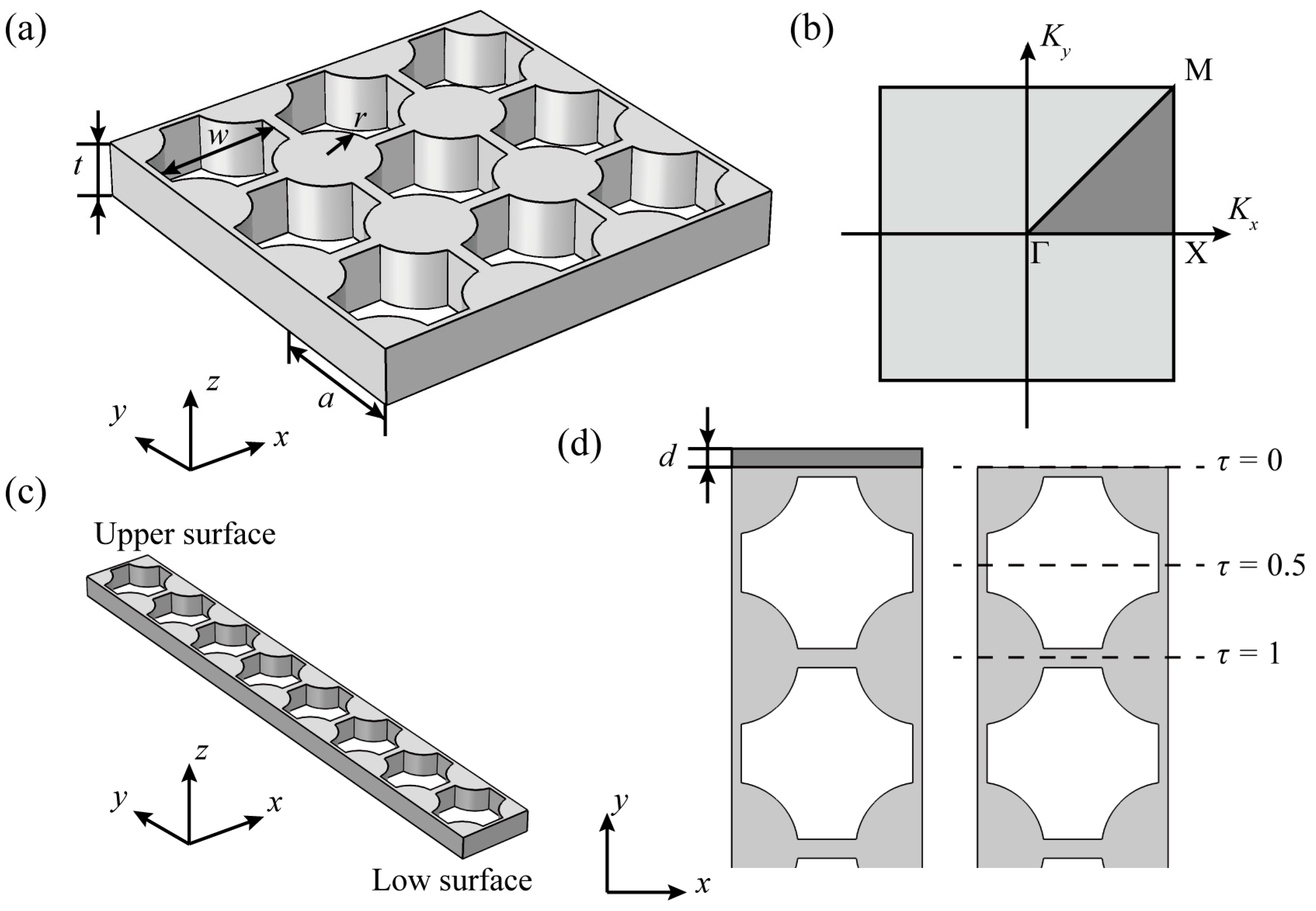
Figure 1a,b shows the PXC slab and the corresponding Brillouin zone, respectively. This structure can be considered as cylinder scatterers connected by thin connectors. Alternatively, it is formed by drilling complex holes in a square lattice in a silicon slab. A similar 2D PXC, which insures simultaneous, large, complete photonic and phononic bandgaps, was investigated previously [36]. Furthermore, now we extend the 2D structure to 2.5D, i.e., a PXC slab. The geometrical parameters are the lattice constant a, cylinder radius r, hole width w, and slab thickness t, respectively. The PXC slab is truncated at both upper and lower surfaces to generate surface waves, as illustrated in Figure 1c. Initially, it has a finite length of 8 unit-cells along the y-axis. For the purpose of modifying the surface bands, we change the upper surface by two ways. The first is adding a silicon layer at the upper surface and varying its thickness d, as the left panel of Figure 1d shows. For the second one, a termination parameter τ (0 ≤ τ ≤ 1) is defined to describe the plane of termination on the surface, see the right panel of Figure 1d. The PXC slab has a finite length of 8 unit-cells along the y-axis with τ = 0 or of 7 unit-cells with τ = 1. Both surface acoustic and surface optical waves propagate along the x-axis, i.e., Γ-X direction.
The material parameters of silicon are the refractive index n = 3.5, mass density ρ = 2331 kg/m3, elastic moduli C11 = C22 = 16.57 × 10¹⁰ N/m2, C12 = 6.39 × 10¹⁰ N/m2, and C44 = 7.962 × 10¹⁰ N/m2, respectively [37]. Throughout this paper, the silicon is assumed to be crystalline with its main symmetry axes aligned to x, y, and z directions of the coordinate system.
With respect to the symmetry of the PXC slab it is possible to impose a symmetry plane, i.e., the middle plane along the slab thickness, to separate photonic modes into even and odd modes. Even (odd) mode is also termed TE-like (TM-like) mode. Then, only one half of the structure needs to be computed for the photonic case. Here, we note that the excitation of even or odd modes can be separately achieved by a proper selection of the polarization of the injected light in a real PTC device. On the other hand, full PNBGs are considered for the phononic case. Unlike a pseudo-bandgap for particular symmetry in the frequency range of definition, a full bandgap can prohibit the propagation of phonons regardless of the mode symmetry and the wave vector. The use of a full PNBG is essential to reduce mechanical losses in the PXC structures [25,27]. In the present work, both phononic and photonic modes are calculated by the finite element method (FEM) (COMSOL Multiphysics). The unit-cell is meshed by second-order tetrahedral elements, and the mesh convergence is confirmed.
3. Slab Modes
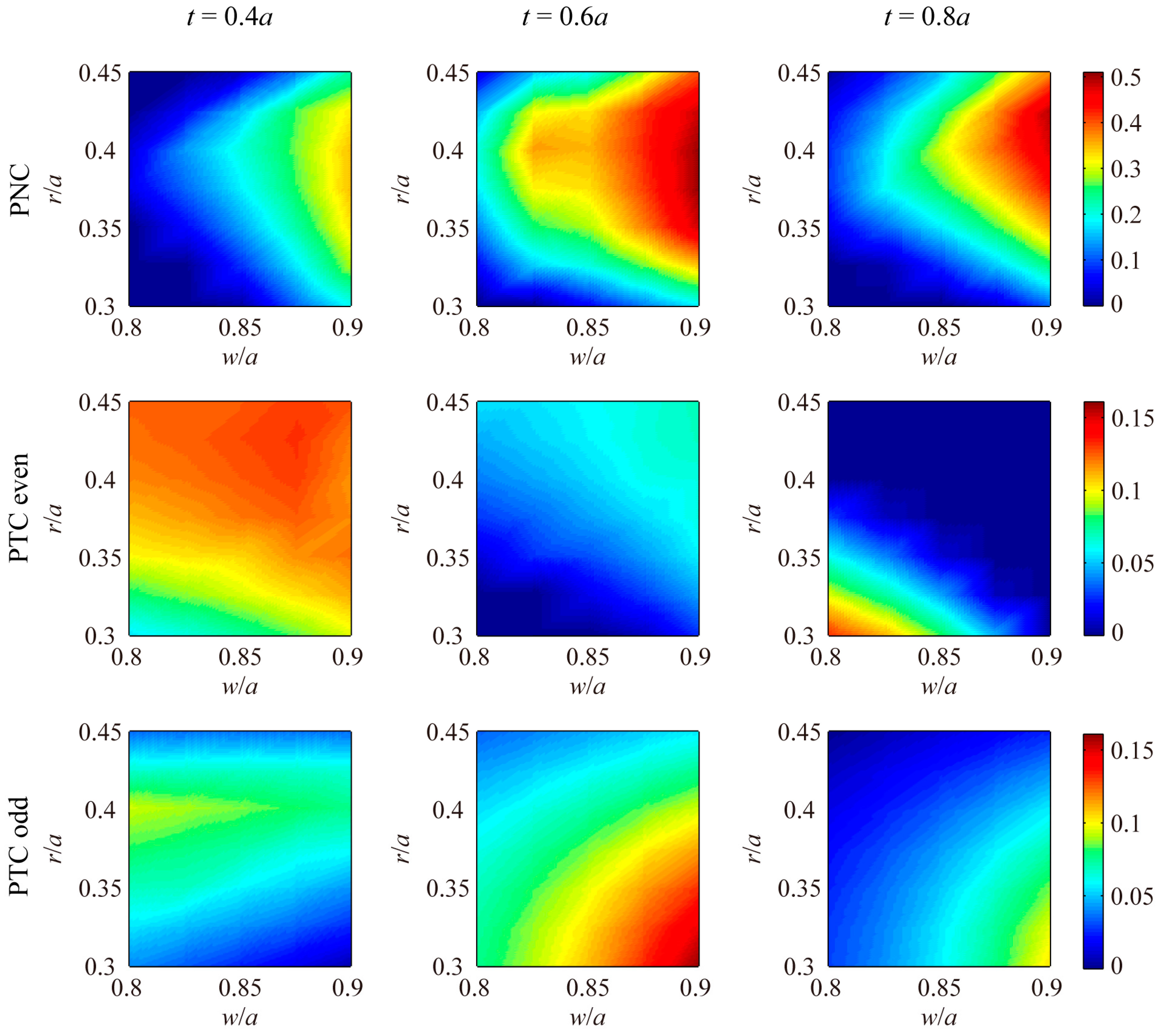
It is noteworthy that a bandgap is the basis of phononic and photonic surface modes because these surface bands appear in bandgaps (the mechanisms of both surface acoustic and optical modes will be discussed in Section 4). So, in this section we need to search simultaneously large phononic and photonic bandgaps by varying the geometrical parameters of a unitcell. It is well known that the slab thickness affects both phononic and photonic band structures significantly, which is different from 2D PXC cases. Figure 2 illustrates the gap-to-midgap ratios of phononic modes (top row) and photonic even (middle row) and odd (bottom row) modes varying with geometrical parameters r and w. Three slab thicknesses, i.e., t = 0.4a, 0.6a, and 0.8a, are considered. The gap-to-midgap ratio is defined by Δω/ωm, where Δω and ωm are the width and central frequency of the bandgap, respectively. The photonic and phononic eigenfrequencies are normalized by 2πc/a and 2πct/a, respectively, with c being the velocity of light in air and ct the elastic transverse wave velocity of the silicon. It is assumed that the surface waves propagate along Γ-X direction. So, only the photonic bandgaps whose upper edge is lower than the normalized frequency of 0.5 are investigated in this paper. This makes the optical surface bands below the light line. The bandgaps shown in Figure 2 are between the 6th and 7th bands for the phononic modes, and 2nd and 3rd, 3rd and 4th bands for the photonic even and odd modes, respectively. We have to indicate that two or more bandgaps may appear in the band structures for some geometrical parameters, and we choose the above bandgaps because they are favorable for generating large phononic and photonic bandgaps. It is seen that the gap-to-midgap ratio for the phononic mode increases with the increase of w. For a given w, this bandgap is widest at an intermediate value of r and becomes narrower as r deviates from this value. When the hole width w = 0.9a, the largest gap-to-midgap ratios exceed 35%, 50%, and 45% for the slab thicknesses t = 0.4a, 0.6a, and 0.8a, respectively. It is easier to obtain a larger phononic bandgap with t = 0.6a than with the other two cases because it exists in a wide geometrical parameter range. When we consider the photonic even mode with t = 0.4a and 0.6a, the bandgap becomes wider along the positive diagonal direction in the gap-to-midgap ratio map, i.e., w and r simultaneously increasing, as plotted in the middle row of Figure 2. On the contrary, with t = 0.8a, the bandgap becomes narrower as w and r simultaneously increase. However, when t = 0.6a, the bandgap is very narrow. So it is hard to obtain large phononic and photonic even mode bandgaps simultaneously for t = 0.6a. It can be observed that for t = 0.8a the large phononic and photonic even mode bandgaps do not overlap in the same geometrical parameter range. Then, simultaneous large bandgaps of phononic and photonic even modes can be obtained only for t = 0.4a. Unlike the photonic even mode, the largest odd mode bandgap, which widens as w increases and r decreases, appears when t = 0.6a. The largest photonic odd mode bandgap has a gap-to-midgap ratio of 16% with r = 0.3a, w = 0.9a, and t = 0.6a. But for t = 0.4a and 0.8a, the gap-to-midgap ratio of the bandgap does not exceeds 10%. Therefore, for phononic and photonic odd modes, we choose t = 0.6a to ensure dual large bandgaps.
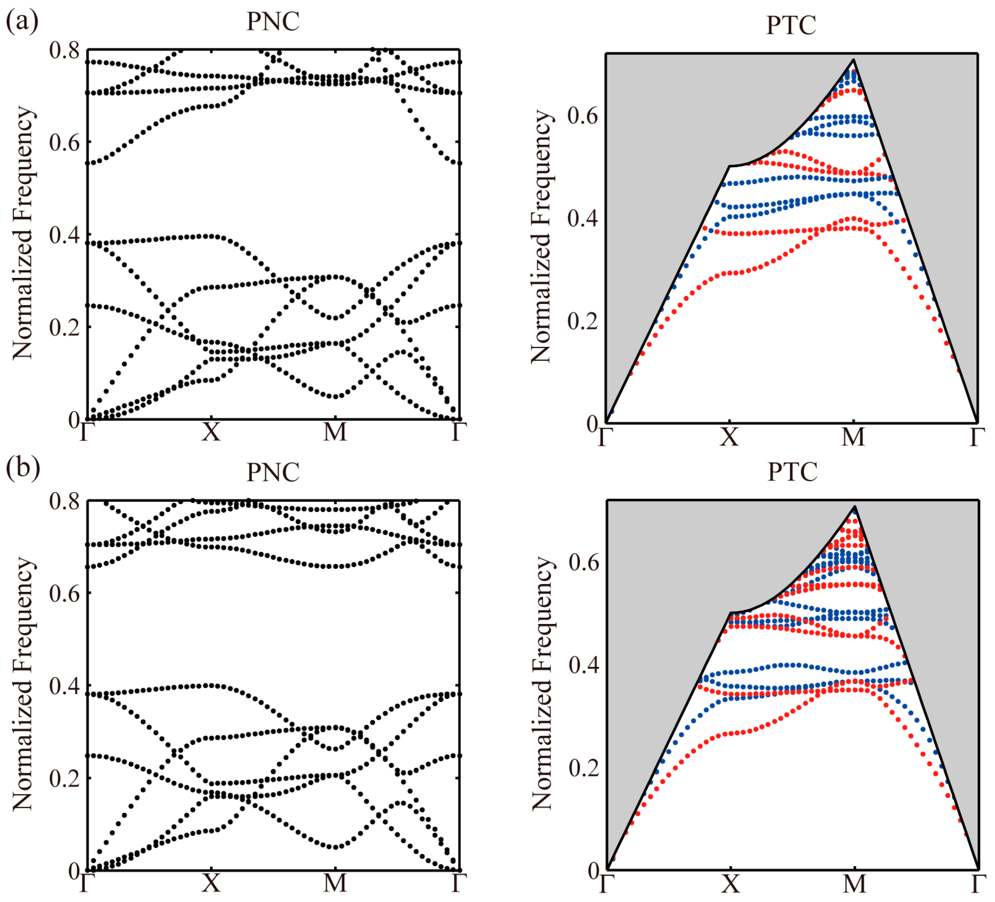
As discussed above, a PXC slab with t = 0.4a (t = 0.6a) benefits the generation of both large bandgaps of phononic and photonic even (odd) modes. For t = 0.4a and t = 0.6a the corresponding phononic and photonic band structures are illustrated in Figure 3a,b respectively, where the other geometrical parameters are r = 0.35a and w = 0.9a. The red and blue dotted lines denote the photonic even and odd modes, respectively. Figure 3a shows the large phononic and photonic even mode bandgaps, while Figure 3b aims shows the large phononic and photonic odd mode ones. One can see that the phononic and photonic even mode bandgaps are of the normalized frequency ranges 0.395 < ωa/2πct < 0.553 (with the gap-to-midgap ratio of 33.3%) and 0.398 < ωa/2πc < 0.449 (with the gap-to-midgap ratio of 12%), respectively. Moreover, two bandgaps for photonic odd modes are exhibited in the band structure. The first bandgap is over the frequency range of 0.448 < ωa/2πc < 0.464. Actually, the second bandgap covers the frequency range of 0.479 < ωa/2πc < 0.552. However, in this work the upper edge of the photonic bandgap has to be lower than the normalized frequency of 0.5, as we indicated previously. Then, this bandgap is characterized by the normalized frequency range of 0.479 < ωa/2πc < 0.5. In Figure 3b, the phononic and photonic odd bandgaps are over 0.398 < ωa/2πct < 0.655 (with the gap-to-midgap ratio of 48.8%) and 0.403 < ωa/2πc < 0.46 (with the gap-to-midgap ratio of 13.2%), respectively. A large photonic even bandgap in the frequency range between 0.37 and 0.392 can be also observed in the band structure. Although the photonic mode is divided into even and odd modes, the bandgaps of even and odd modes can appear in the same PXC structure, as shown in the photonic band structures. The investigation of surface modes in the next section is based on the unitcell with the above geometrical parameters.
In view of practical application, the photonic operating wavelength λ is about 1550 nm. If the central frequency of photonic bandgap is chosen as the operating frequency, for the photonic even (odd) mode the corresponding geometrical parameters are a = 656 (669) nm, r = 229.6 (234.15) nm, w = 590.4 (602.1) nm, and t = 262.4 (401.4) nm, respectively. In turn, the central frequency of the phononic bandgap corresponding to photonic even (odd) mode is 4.22 (4.6) GHz.
4. Surface Modes
In this work the PXC slab possesses the same upper and lower surfaces. Additionally, due to the structure symmetry with respect to the plane y = 0, all surface acoustic and optical bands appear in pairs. One surface mode is localized at the upper surface, and another one with the same frequency is localized at the lower surface. If the surface bands are at a distance from the light line (for light waves) and the bandgap edges, the upper and lower surface modes cannot couple to each other, because there are enough periods of the PXCs in the interior region, that is to say, with the upper surface geometrical parameters changing the upper surface bands vary, while the lower ones keep invariant. So, only the upper surface bands will be plotted in the band diagrams. The generation of SOWs is due to the total internal reflection and the PTBG effect. For SAWs we assume that the acoustic waves (elastic waves) in solids cannot radiate into the air region from the free surfaces. Additionally, due to the existence of the PNBG, they cannot propagate from the surface into the interior space. So, the SAWs here are different from the traditional SAWs (for example, Rayleigh wave) in PNCs, and the sound line will not be illustrated.
4.1. Phononic and Photonic Even Modes
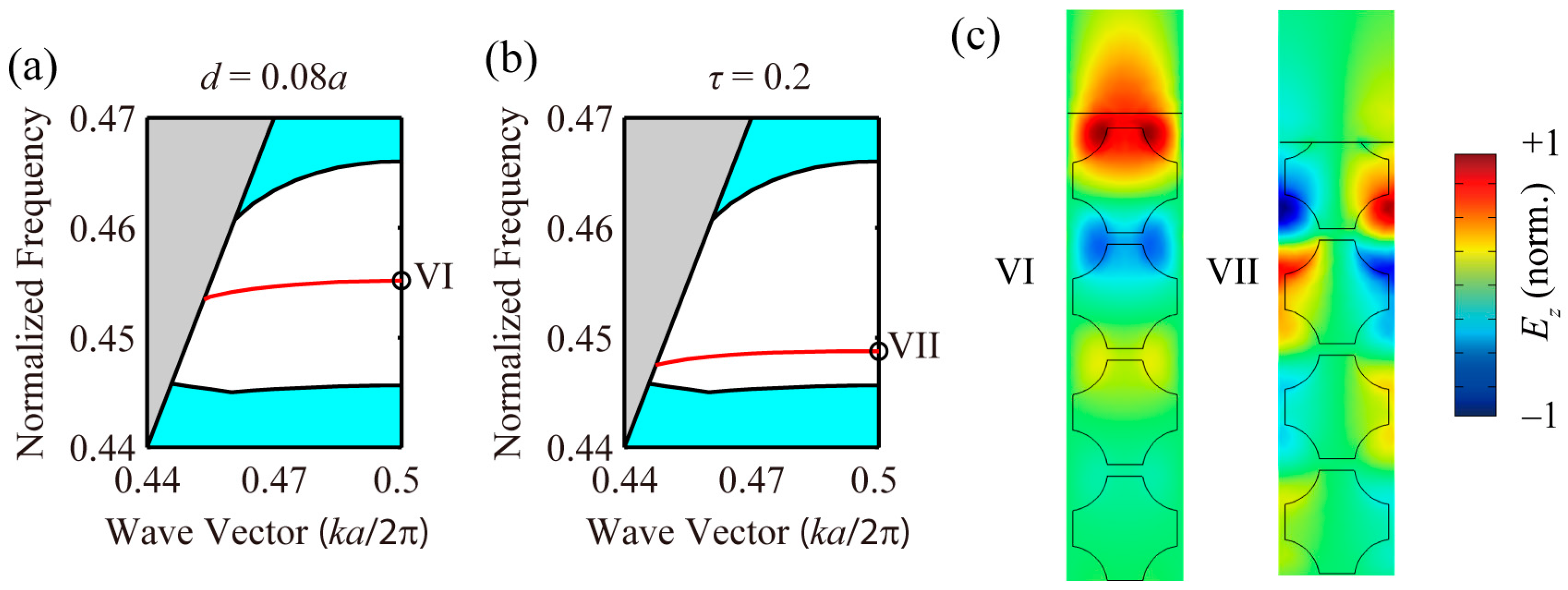
We take the geometrical parameters of the unitcell as r = 0.35a, w = 0.9a, and t = 0.4a. As indicated previously, two methods are adopted here to tune the surface bands. At first, we change the additional layer thickness d and show the dispersion curves of the surface wave bands of phononic and photonic even modes in Figure 4. For PNCs, when d = 0 (alternately could be considered as τ = 0), four surface bands can be observed in the band structure. The lowest band is impractical because it is very close to the edge of the projected bulk mode and is not located in the bandgap. The other three bands move toward the upper bandgap edge as d increases and are out of the PNBG when d = 0.04a. Though these bands do not locate in the complete bandgap, the corresponding surface modes actually exist, as the modal distribution at point c shows. With the layer thickness d increasing, two surface acoustic bands gradually rise from the lower edge of the bandgap. Here we have to note that surface bands, e.g., the lower two surface bands with d = 0.12a, which appear in the complete bandgap, are preferable. Two SAW bandgaps exist with d = 0, where the upper one disappears when d reaches 0.04a. Then, only one large SAW bandgap appears when d varies from 0.04a to 0.16a. This bandgap becomes narrower with the increase of d owing to the rising of its lower edge (the lower surface band) and the invariance of its upper edge. The SAW bandgap covers the frequency ranges of 0.433 < ωa/2πct < 0.557 and 0.49 < ωa/2πct < 0.557 for d = 0.04a and d = 0.16a, respectively. For photonic case one, SOW band, which shifts toward lower frequencies with d increasing from 0 to 0.16a, can be found in the complete PTBG. The PTBG is divided into two SOW bandgaps by this SOW branch. However, this surface band is quite flat and then these two SOW bandgaps can be considered as an entire one (0.398 < ωa/2πc < 0.487), inside which a flat surface band bandwidth exists. In Figure 4c, the acoustic deformation modes at points a and b correspond to the z- and x-directional vibrations of the cylinder scatterers, respectively, and at point c correspond to the vibration of the connectors along the y-axis. From Figure 4d, we can see that point 1 is closer to the upper bandgap edge than point 2, and this makes more optical waves radiate into the interior region at point 1 than at point 2. This SOW band is a dielectric band, as most of the energy is confined in the silicon region. For the surface mode bands, both acoustic and optical waves can be highly localized near the surface and attenuate exponentially away from the surface, as the modal distribution confirms. It is noteworthy that joint surface bands and surface wave bandgaps are fundamental to the design of various PXC devices in order to simultaneously manipulate surface acoustic and optical waves.
As the termination parameter τ varies, the dispersion curves of the surface wave bands of phononic and photonic even modes are shown in Figure 5. We change τ from 0.05 to 0.2 with a step of 0.05. From τ = 0.05, the thin connectors between the cylindrical scatterers at the upper surface no longer exist, and these scatterers can be regarded as individual resonators for the case of a PNC. One surface acoustic band appears in the complete PNBG and goes up with τ increasing, as displayed in Figure 5a. Moreover, this surface band is quite flat and corresponds to the locally resonant mode of the resonators, as shown by the deformation pattern in Figure 5c. The resonators at the upper surface vibrate almost in yz-plane, while the rest parts of the structure are still. Similar to the acoustic mode, there is one optical surface band appearing in the complete PTBG, and this band rises slightly as τ increases. From the modal distribution in Figure 5d, it can be seen that the maximum magnetic field locates at the top of the second row of the PXC slab, and that the optical waves attenuate away from this region. This surface band is an air band, as most of the energy concentrates in the air region. Additionally, from Figure 5 it is obviously seen that single phononic/photonic guided mode exists inside the bandgap, so that the intermodal coupling can be neglected.
In Figure 5a the surface acoustic bands are flat, as we indicated previously; the flatness of the bands implies a small value of the group velocity. Slow wave effects can significantly enhance the AO coupling, light-matter interaction for sensing, and the nonlinear effects in PXC structures [38,39,40]. The group velocity is defined as
In the photonic case, it is customary to consider the group index given by ng = c/vg. In parallel, we can define an equivalent group index in the phononic case as ng = ct/vg. Another criterion for evaluating the performance of the slow wave effect is group velocity dispersion (GVD). A large GVD can lead to serious distortion and broadening of the pulse along a waveguide due to the dispersion of the spectral components with different speeds. In addition, pulse broadening can lower the peak intensity of a pulse and then reduce the nonlinear effects. The GVD can be estimated from the dispersion relations through the definition as follows
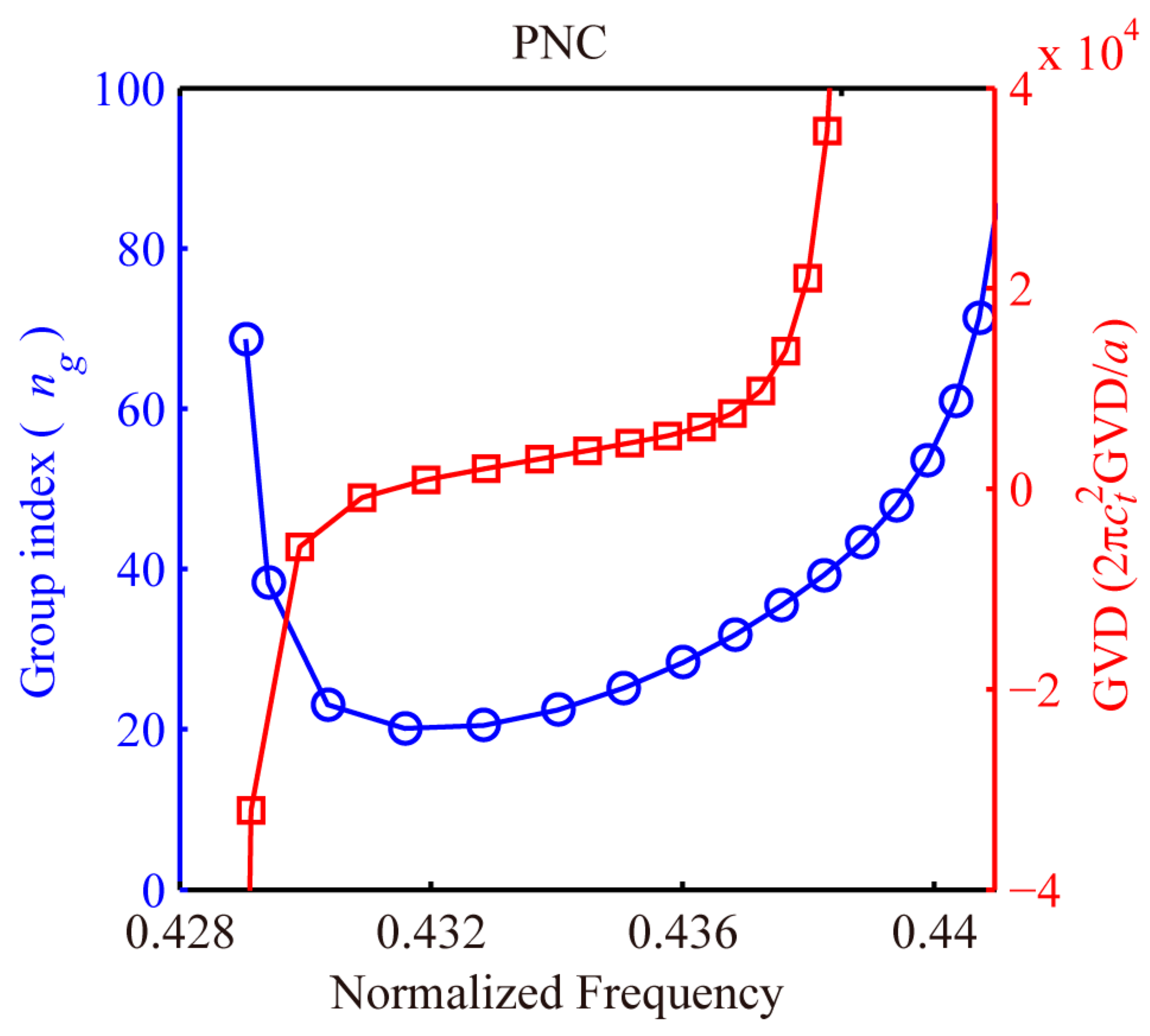
Considering the practical application requirement, we should take the GVD value lower than 104a/2πc2 [41,42]. The group index and GVD as functions of the frequency for the surface acoustic band marked with yellow color in Figure 5a are shown in Figure 6. The group index curve displays a U-shape with a minimum value of 20, which means the group velocity is more than 20 times less than the speed of the bulk transverse wave in silicon. It is noted that the GVD condition (–104a/2πct2 < GVD < 104a/2πct2) is satisfied in the frequency range of 0.43 < ωa/2πct < 0.44, where the group index varies from 20 to 47. However, in the same geometrical configuration no surface optical band with a small group velocity can be obtained.
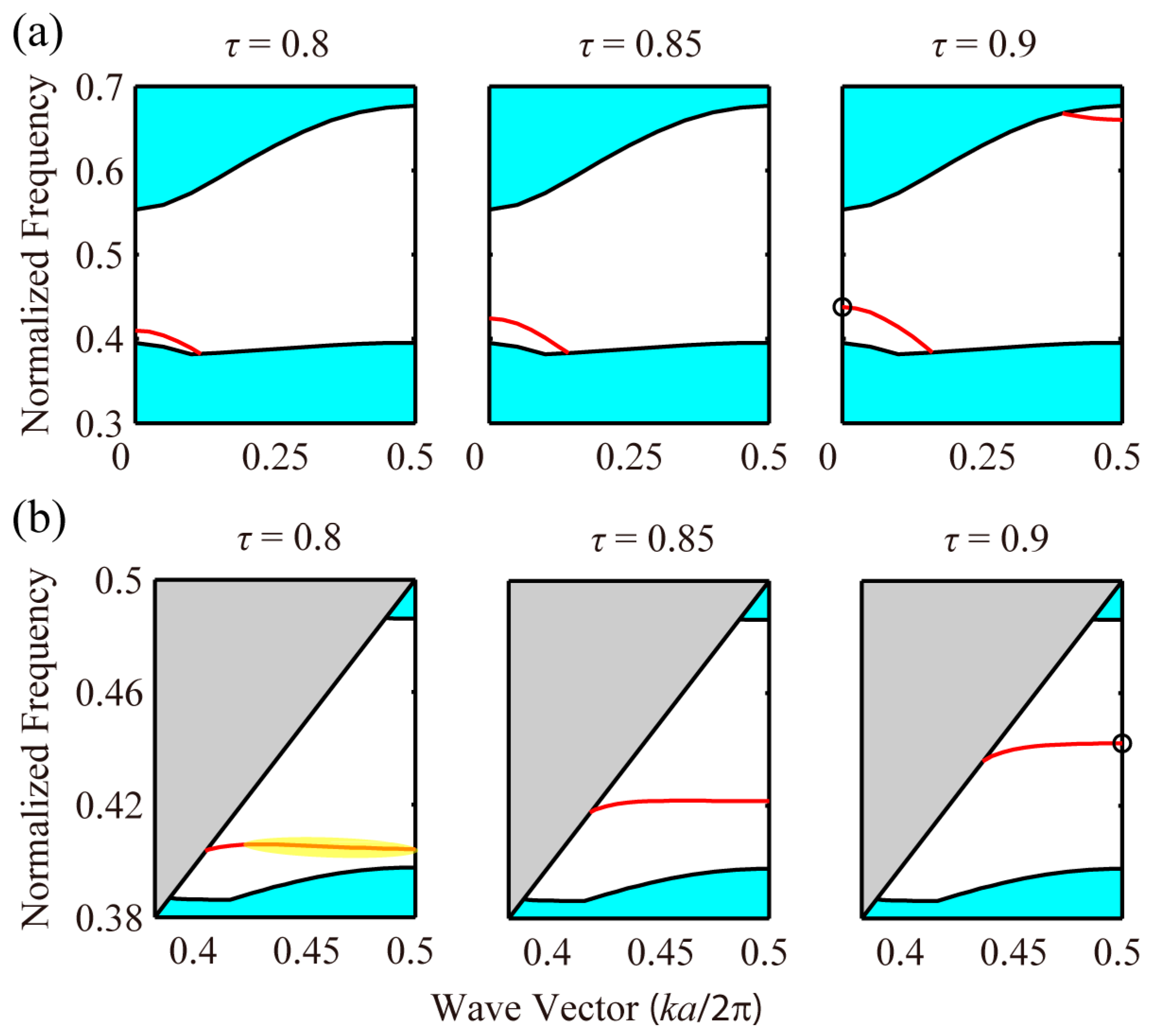
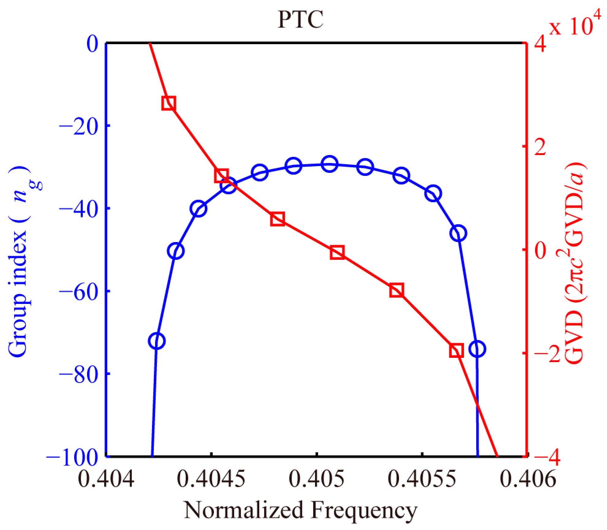
Figure 7 plots the phononic and photonic band structures with the termination parameter τ = 0.8–0.9. This PXC structure is similar to that with an additional layer, and may be considered as covering a thin layer with different shapes at the surface. For both phononic and photonic crystals, one surface band, whose frequency increases with τ increasing, appears in the bandgap. Furthermore, simultaneously large phononic and photonic bandgaps of the surface waves can be obtained. For instance, with τ being 0.9, the PNBG takes the frequency range of 0.438 < ωa/2πct < 0.558 (gap-to-midgap ratio = 24.1%), while two PTBGs take those of 0.398 < ωa/2πc < 0.436 (gap-to-midgap ratio = 9.1%) and 0.442 < ωa/2πc < 0.486 (gap-to-midgap ratio = 9.5%), respectively. The variations of the group index and GVD with the frequency for the surface optical band marked with yellow in Figure 7b are illustrated in Figure 8. As the frequency increases, the absolute value of the group index first decreases to the minimum value of 29 and then increases. With a small GVD, the corresponding group index is between 29 and 30.5. Unfortunately, only the SOWs can be slowed down with these surface parameters, while the slow wave effects are not significant for the SAWs.
For the phononic and photonic even modes, the surface waves propagating along the surface of truncated PXC slabs are investigated in this section. The results show that the bandgaps for surface waves can be tuned by changing the surface parameters. The acoustic and optical single-modes can be simultaneously achieved by adjusting the surface geometrical parameters. For the slow wave effect, it is hard to realize simultaneously slow sound and light by simple modification of the surface structures.
4.2. Phononic and Photonic Odd Modes
We take the geometrical parameters of the unitcell as follows, r = 0.35a, w = 0.9a, and t = 0.6a. At first, the effect of d on the surface acoustic and optical waves in the PXC slab is investigated, see Figure 9. There are five surface acoustic bands in the PNBG when d is 0, see Figure 9a. These surface bands go upward as d increases; among them, the upper three bands disappear, with d reaching 0.04a. Moreover, another two bands generate from the bottom of the PNBG and also rise up with the increase of d. For all of these surface parameters, one or two SAW bandgaps can be observed. The acoustic energy is highly confined at the surface region because SAWs cannot propagate into the second row of the PXC slab, as shown by the displacement field in Figure 9c. For the photonic case, three SOW bands appear when d = 0 and drop down with d increasing. The PTBG is separated by these surface bands into two or three SOW bandgaps. The lower tow branches fall below the lower PTBG edge when d reaches 0.04a and 0.12a, respectively. Additionally, from d = 0.12a one can see the presence of a single SOW mode in the PTBG. It can be seen from Figure 9d that more optical energy penetrates into the air region at point I, while most of the energy is confined in silicon at points II and III. So, the surface band corresponding to point I is an air band, and the other two corresponding to points II and III are dielectric bands.
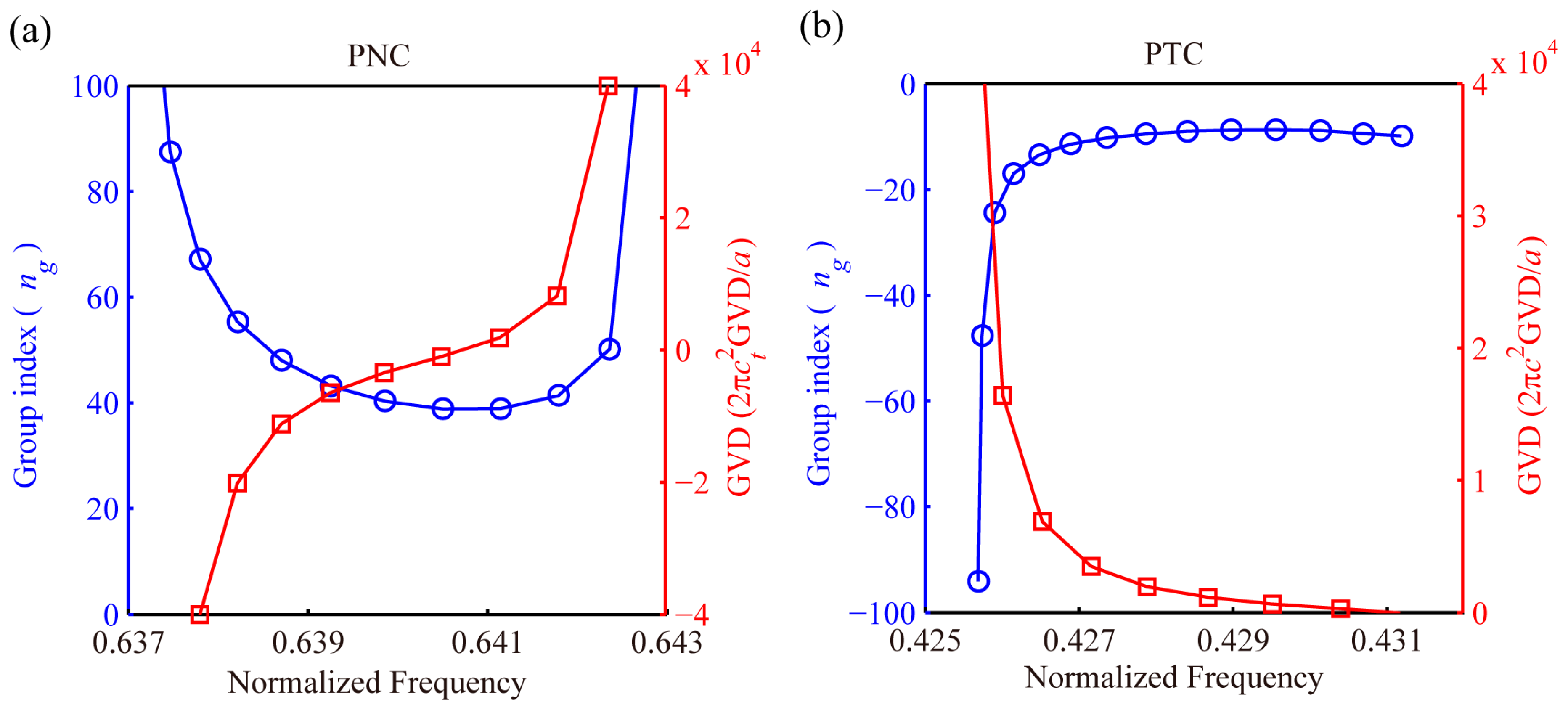
Figure 10 displays the dependences of the group index and GVD with the normalized frequency for the surface acoustic and optical bands marked with yellow color in Figure 9a,b. For the phononic case, a U-shape in the group index curve is exhibited, and around the normalized frequency ωa/2πct = 0.6405, the group index remains approximately constant (ng = 39). Meanwhile, the corresponding absolute value of GVD is between 0 and 8×10³a/2πct2. In Figure 10b, there is a flat region in the group index curve for a wide frequency range between 0.427 and 0.431, where the group index and GVD for the optical waves are smaller than −8.6 and 4×10³a/2πc2, respectively. Additionally, in this case, simultaneously slow SAWs and SOWs with a small GVD can be achieved, which is different from those cases discussed in Section 4.1, where only acoustic or optical waves can be slowed down.
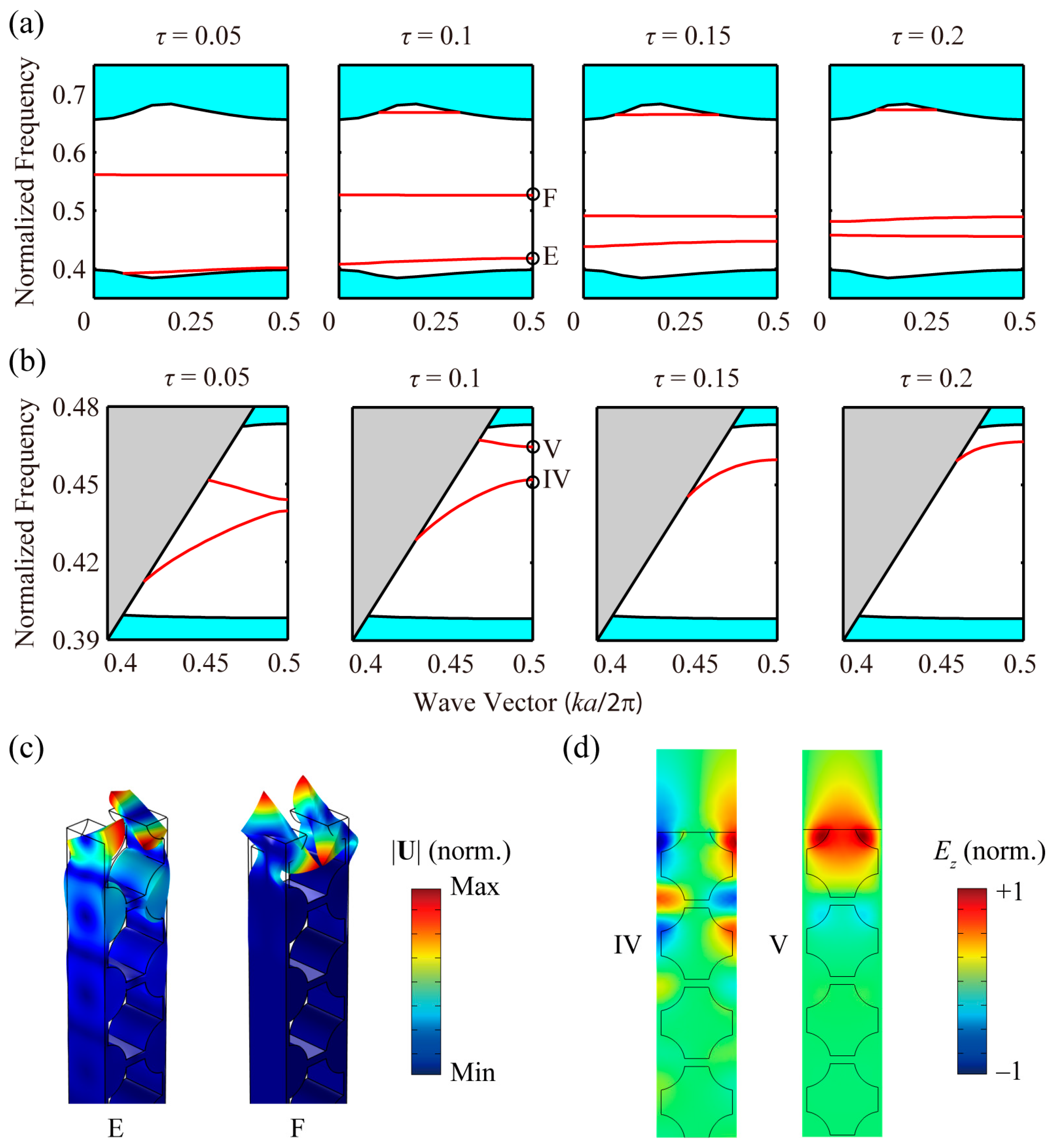
The variations of the surface mode branches with the termination parameter τ are illustrated in Figure 11. Two flat SAW bands are exhibited in the PNBG, among which the upper one shifts toward the lower frequency as τ increases, while the lower one behaves conversely. The vibration modes corresponding to these bands are locally resonant modes. The vibration mode at point E shows almost the swing of the resonators in the yz-plane, and at point F the resonators vibrate in the yz-plane as well as twist slightly on the y-axis, as plotted in Figure 11c. As the slopes of both surface acoustic bands are very low, it can be inferred that these bands possess high group indices. There are two SOW bands appearing in the PTBG when τ = 0.05. Both of them move up as τ increases and the upper one moves out of the PTBG when τ = 0.15. The PTBG is separated by these bands into two or three SOW bandgaps. The lower and upper bands are dielectric and air bands, respectively. The optical energy is well localized in the upper surface region at points IV and V, as depicted in Figure 11d. When τ varies from 0.8 to 0.9, the bands and bandgaps of the surface acoustic and optical modes can be observed in the band structures, as shown in Figure 12. The behaviors of these surface modes are similar to those in Figure 9 and will not be discussed in detail.
4.3. Phononic, Photonic Even and Odd Modes
The dispersion curves of the photonic odd modes with the geometrical parameters r = 0.35a, w = 0.9a, t = 0.4a, d = 0.04a (a), and τ = 0.2 (b) are shown in Figure 13. We have indicated that in the same PXC slab, dual phononic and photonic even surface modes can appear in the bandgaps, see Figure 4 and Figure 5. Although with these geometrical parameters the photonic odd bandgap is not as large as that of the even mode, the bands and bandgaps of the surface optical odd modes exist with two different surface configurations, as illustrated in Figure 13. Moreover, the modal distributions show the electric field attenuates fast away from the structure surface. Consequently, we indicate that simultaneous presences of surface acoustic, optical even, and odd modes can be achieved in the same PXC slab.
5. Conclusions
The opening of simultaneous phononic and photonic bandgaps in PXC slabs with veins is theoretically studied. Dual large bandgaps of phononic and photonic even/odd modes can be obtained over a wide range of geometry parameters, which provides good tolerance for the technological realization and flexibility of designing this PXC structure. Based on these large bandgaps, simultaneous guidance of SAWs and SOWs along the surface of truncated PXC slabs is demonstrated. The bandgaps of surface waves, as well as the surface bands, can be tuned effectively through changing the surface geometrical parameters. Moreover, the acoustic and optical single-modes can be simultaneously achieved by properly adjusting the surface geometrical parameters, which is beneficial for the waveguide applications. Slow wave effects with small GVD for the SAW or/and SOW are found. For the phononic and photonic even modes, the slow wave effects for the SAW of SOW can be realized. However, for the phononic and photonic odd modes, the SAW and SOW can be simultaneously slowed down, where the acoustic and optical group velocities as small as ct/40 and c/10 are predicted, respectively. The PXC slabs can be applied for the design of highly sensitive parallel sensors or the integration of PXC devices.
In the present work, we especially focus our study on tuning the SAW and SOW bands, as well as the surface mode bandgaps. We do not further change the configuration of the PXC slab surface to improve the slow wave effects of these surface bands. As numerous attempts have been devoted to slow down light or sound in the PTC [43] or PNC [44,45] structures, it can be inferred that by finely tuning the geometrical parameters, the improvement of simultaneously slow sound and light can be realized in this kind of PXC structure. We believe the PXC surface waveguides can be adopted to study the optomechanical/acousto-optical interaction between the photonic and phononic guided modes [46,47,48]. The development of the waveguides supporting the propagation of slow photons and phonons at the same time may result in the enhancement of the photon-phonon interaction. Additionally, the optomechanical coupling in the surface waveguides could be compared with that in the standard silicon waveguides. Last but not least, these results may potentially stimulate additional design rules for new topological insulators in optomechanics [49,50].
Acknowledgments
This work was supported by the National Natural Science Foundation (11372031, 11532001) and Joint Sino-German Research Project (Grant No. GZ 1355).
Author Contributions
Tian-Xue Ma designed and performed the simulations; Tian-Xue Ma, Yue-Sheng Wang and Chuanzeng Zhang discussed the results; Yue-Sheng Wang and Chuanzeng Zhang supervised the research; Tian-Xue Ma, Yue-Sheng Wang and Chuanzeng Zhang prepared and wrote the paper.
Conflicts of Interest
The authors declare no conflict of interest.
References
- Pennec, Y.; Laude, V.; Papanikolaou, N.; Djafari-Rouhani, B.; Oudich, M.; El Jallal, S.; Beugnot, J.C.; Escalante, J.M.; Martínez, A. Modeling light-sound interaction in nanoscale cavities and waveguides. Nanophotonics 2014, 3, 413–440. [Google Scholar] [CrossRef]
- Maldovan, M.; Thomas, E.L. Simultaneous localization of photons and phonons in two-dimensional periodic structures. Appl. Phys. Lett. 2006, 88, 251907. [Google Scholar] [CrossRef]
- Maldovan, M.; Thomas, E.L. Simultaneous complete elastic and electromagnetic band gaps in periodic structures. Appl. Phys. B 2006, 83, 595–600. [Google Scholar] [CrossRef]
- Sadat-Saleh, S.; Benchabane, S.; Baida, F.I.; Bernal, M.P.; Laude, V. Tailoring simultaneous photonic and phononic band gaps. J. Appl. Phys. 2009, 106, 074912. [Google Scholar] [CrossRef]
- Papanikolaou, N.; Psarobas, I.E.; Stefanou, N. Absolute spectral gaps for infrared light and hypersound in three-dimensional metallodielectric phoxonic crystals. Appl. Phys. Lett. 2010, 96, 231917. [Google Scholar] [CrossRef] [Green Version]
- Mohammadi, S.; Eftekhar, A.A.; Khelif, A.; Adibi, A. Simultaneous two-dimensional phononic and photonic band gaps in opto-mechanical crystal slabs. Opt. Express 2010, 18, 9164–9172. [Google Scholar] [CrossRef] [PubMed]
- Ma, T.X.; Wang, Y.S.; Wang, Y.F.; Su, X.X. Three-dimensional dielectric phoxonic crystals with network topology. Opt. Express 2013, 21, 2727–2732. [Google Scholar] [CrossRef] [PubMed]
- Rolland, Q.; Dupont, S.; Gazalet, J.; Kastelik, J.C.; Pennec, Y.; Djafari-Rouhani, B.; Laude, V. Simultaneous bandgaps in LiNbO3 phoxonic crystal slab. Opt. Express 2014, 22, 16288–16297. [Google Scholar] [CrossRef] [PubMed]
- Dong, H.W.; Wang, Y.S.; Ma, T.X.; Su, X.X. Topology optimization of simultaneous photonic and phononic bandgaps and highly effective phoxonic cavity. J. Opt. Soc. Am. B 2014, 31, 2946–2955. [Google Scholar] [CrossRef]
- Laude, V.; Beugnot, J.C.; Benchabane, S.; Pennec, Y.; Djafari-Rouhani, B.; Papanikolaou, N.; Escalante, M.; Martinez, A. Simultaneous guidance of slow photons and slow acoustic phonons in silicon phoxonic crystal slabs. Opt. Express 2011, 19, 9690–9698. [Google Scholar] [CrossRef] [PubMed] [Green Version]
- Escalante, J.M.; Martínez, A.; Laude, V. Design of single-mode waveguides for enhanced light-sound interaction in honeycomb-lattice silicon slabs. J. Appl. Phys. 2014, 115, 064302. [Google Scholar] [CrossRef]
- Lucklum, R.; Zubtsov, M.; Oseev, A. Phoxonic crystals-a new platform for chemical and biochemical sensors. Anal. Bioanal. Chem. 2013, 405, 6497–6509. [Google Scholar] [CrossRef] [PubMed]
- Amoudache, S.; Pennec, Y.; Djafari Rouhani, B.; Khater, A.; Lucklum, R.; Tigrine, R. Simultaneous sensing of light and sound velocities of fluids in a two-dimensional phoXonic crystal with defects. J. Appl. Phys. 2014, 115, 134503. [Google Scholar] [CrossRef]
- Amoudache, S.; Moiseyenko, R.; Pennec, Y.; Djafari Rouhani, B.; Khater, A.; Lucklum, R.; Tigrine, R. Optical and acoustic sensing using Fano-like resonances in dual phononic and photonic crystal plate. J. Appl. Phys. 2016, 119, 114502. [Google Scholar] [CrossRef] [Green Version]
- Ma, T.X.; Wang, Y.S.; Zhang, C.; Su, X.X. Theoretical research on a two-dimensional phoxonic crystal liquid sensor by utilizing surface optical and acoustic waves. Sens. Actuators A 2016, 242, 123–131. [Google Scholar] [CrossRef]
- Chen, G.; Zhang, R.; Sun, J. On-chip optical mode conversion based on dynamic grating in photonic-phononic hybrid waveguide. Sci. Rep. 2015, 5, 10346. [Google Scholar] [CrossRef] [PubMed]
- Chen, J.J.; Huo, S.Y. Investigation of dual acoustic and optical asymmetric propagation in two-dimensional phoxonic crystals with grating. Opt. Mater. Express 2017, 7, 1716–1724. [Google Scholar] [CrossRef]
- Almpanis, E.; Papanikolaou, N.; Stefanou, N. Breakdown of the linear acousto-optic interaction regime in phoxonic cavities. Opt. Express 2014, 22, 31595–31607. [Google Scholar] [CrossRef] [PubMed]
- Kipfstuhl, L.; Guldner, F.; Riedrich-Möller, J.; Becher, C. Modeling of optomechanical coupling in a phoxonic crystal cavity in diamond. Opt. Express 2014, 22, 12410–12423. [Google Scholar] [CrossRef] [PubMed]
- Hsu, J.C.; Lu, T.Y.; Lin, T.R. Acousto-optic coupling in phoxonic crystal nanobeam cavities with plasmonic behavior. Opt. Express 2015, 23, 25814–25826. [Google Scholar] [CrossRef] [PubMed]
- Huang, Z.; Cui, K.; Li, Y.; Feng, X.; Liu, F.; Zhang, W.; Huang, Y. Strong Optomechanical Coupling in Nanobeam Cavities based on Hetero Optomechanical Crystals. Sci. Rep. 2015, 5, 15964. [Google Scholar] [CrossRef] [PubMed]
- Chiu, C.C.; Chen, W.M.; Sung, K.W.; Hsiao, F.L. High-efficiency acousto-optic coupling in phoxonic resonator based on silicon fishbone nanobeam cavity. Opt. Express 2017, 25, 6076–6091. [Google Scholar] [CrossRef] [PubMed]
- Eichenfield, M.; Chan, J.; Camacho, R.M.; Vahala, K.J.; Painter, O. Optomechanical crystals. Nature 2009, 462, 78–82. [Google Scholar] [CrossRef] [PubMed]
- Psarobas, I.E.; Papanikolaou, N.; Stefanou, N.; Djafari-Rouhani, B.; Bonello, B.; Laude, V. Enhanced acousto-optic interactions in a one-dimensional phoxonic cavity. Phys. Rev. B 2010, 82, 174303. [Google Scholar] [CrossRef] [Green Version]
- Gomis-Bresco, J.; Navarro-Urrios, D.; Oudich, M.; El-Jallal, S.; Griol, A.; Puerto, D; Chavez, E.; Pennec, Y.; Djafari-Rouhani, B.; Alzina, F.; et al. A one-dimensional optomechanical crystal with a complete phononic band gap. Nat. Commun. 2014, 5, 4452. [Google Scholar] [CrossRef] [PubMed]
- Sun, X.; Zheng, J.; Poot, M.; Wong, C.W.; Tang, H.X. Femtogram doubly clamped nanomechanical resonators embedded in a high-Q two-dimensional photonic crystal nanocavity. Nano Lett. 2012, 12, 2299–2305. [Google Scholar] [CrossRef] [PubMed]
- Safavi-Naeini, A.H.; Hill, J.T.; Meenehan, S.; Chan, J.; Gröblacher, S.; Painter, O. Two-dimensional phononic-photonic band gap optomechanical crystal cavity. Phys. Rev. Lett. 2014, 112, 153603. [Google Scholar] [CrossRef] [PubMed]
- Yu, T.; Wang, Z.; Liu, W.; Wang, T.; Liu, N.; Liao, Q. Simultaneous large band gaps and localization of electromagnetic and elastic waves in defect-free quasicrystals. Opt. Express 2016, 24, 7951–7959. [Google Scholar] [CrossRef] [PubMed]
- Wang, Z.; Liu, W.; Yu, T.; Wang, T. Simultaneous localization of photons and phonons within the transparency bands of LiNbO3 phoxonic quasicrystals. Opt. Express 2016, 24, 23353–23360. [Google Scholar] [CrossRef] [PubMed]
- Ishizaki, K.; Noda, S. Manipulation of photons at the surface of three-dimensional photonic crystals. Nature 2009, 460, 367–370. [Google Scholar] [CrossRef] [PubMed]
- Rahachou, A.I.; Zozoulenko, I.V. Waveguiding properties of surface states in photonic crystals. J. Opt. Soc. Am. B 2006, 23, 1679–1683. [Google Scholar] [CrossRef]
- Kramper, P.; Agio, M.; Soukoulis, C.M.; Birner, A.; Müller, F.; Wehrspohn, R.B.; Gösele, U.; Sandoghdar, V. Highly directional emission from photonic crystal waveguides of subwavelength width. Phys. Rev. Lett. 2004, 92, 113903. [Google Scholar] [CrossRef] [PubMed]
- Lu, T.W.; Hsiao, Y.H.; Ho, W.D.; Lee, P.T. High-index sensitivity of surface mode in photonic crystal hetero-slab-edge microcavity. Opt. Lett. 2010, 35, 1452–1454. [Google Scholar] [CrossRef] [PubMed]
- Hsu, J.C.; Hsu, C.H. Edge waves and resonances in two-dimensional phononic crystal plates. J. Appl. Phys. 2015, 117, 174504. [Google Scholar] [CrossRef]
- Ma, T.X.; Kui, Z.; Wang, Y.S.; Zhang, C.; Su, X.X. Acousto-optical interaction of surface acoustic and optical waves in a two-dimensional phoxonic crystal hetero-structure cavity. Opt. Express 2014, 22, 28443–28451. [Google Scholar] [CrossRef] [PubMed]
- Ma, T.X.; Wang, Y.S.; Zhang, C. Investigation of dual photonic and phononic bandgaps in two-dimensional phoxonic crystals with veins. Opt. Commun. 2014, 312, 68–72. [Google Scholar] [CrossRef]
- El-jallal, S.; Oudich, M.; Pennec, Y.; Djafari-Rouhani, B.; Makhoute, A.; Rolland, Q.; Dupont, S.; Gazalet, J. Optomechanical interactions in two-dimensional Si and GaAs phoXonic cavities. J. Phys. Condens. Matter 2014, 26, 015005. [Google Scholar] [CrossRef] [PubMed]
- Courjal, N.; Benchabane, S.; Dahdah, J.; Ulliac, G.; Gruson, Y.; Laude, V. Acousto-optically tunable lithium niobate photonic crystal. Appl. Phys. Lett. 2010, 96, 131103. [Google Scholar] [CrossRef]
- Hsiao, F.L.; Hsieh, C.Y.; Hsieh, H.Y.; Chiu, C.C. High-efficiency acousto-optical interaction in phoxonic nanobeam waveguide. Appl. Phys. Lett. 2012, 100, 171103. [Google Scholar] [CrossRef]
- Lin, T.R.; Lin, C.H.; Hsu, J.C. Enhanced acousto-optic interaction in two-dimensional phoxonic crystals with a line defect. J. Appl. Phys. 2013, 113, 053508. [Google Scholar] [CrossRef]
- Hou, J.; Gao, D.S.; Wu, H.M.; Hao, R.; Zhou, Z.P. Flat band slow light in symmetric line defect photonic crystal waveguides. IEEE Photonics Technol. Lett. 2009, 21, 1571–1573. [Google Scholar]
- Xu, Y.M.; Xiang, L.; Cassan, E.; Gao, D.S.; Zhang, X.L. Slow light in an alternative row of ellipse-hole photonic crystal waveguide. Appl. Opt. 2013, 52, 1155–1160. [Google Scholar] [CrossRef] [PubMed]
- Baba, T. Slow light in photonic crystals. Nat. Photonics 2008, 2, 465–473. [Google Scholar] [CrossRef]
- Cicek, A.; Kaya, O.A.; Yilmaz, M.; Ulug, B. Slow sound propagation in a sonic crystal linear waveguide. J. Appl. Phys. 2012, 111, 013522. [Google Scholar] [CrossRef]
- Malfanti, I.; Taschin, A.; Bartolini, P.; Torre, R. Evidence of slow acoustic surface waves on a 1D phononic surface by a pulsed laser spectroscopic technique resolved in time and space. EPL 2012, 97, 44010. [Google Scholar] [CrossRef]
- Qiu, W.; Rakich, P.T.; Shin, H.; Dong, H.; Soljačić, M.; Wang, Z. Stimulated Brillouin scattering in nanoscale silicon step-index waveguides: A general framework of selection rules and calculating SBS gain. Opt. Express 2013, 21, 31402–31419. [Google Scholar] [CrossRef] [PubMed]
- Van Laer, R.; Baets, R.; Van Thourhout, D. Unifying Brillouin scattering and cavity optomechanics. Phys. Rev. A 2016, 93, 053828. [Google Scholar] [CrossRef]
- Zhang, R.; Sun, J. Design of silicon phoxonic crystal waveguides for slow light enhanced forward stimulated Brillouin scattering. J. Lightwave Technol. 2017, 35, 2917–2925. [Google Scholar] [CrossRef]
- Peano, V.; Brendel, C.; Schmidt, M.; Marquardt, F. Topological Phases of Sound and Light. Phys. Rev. X 2015, 5, 031011. [Google Scholar] [CrossRef]
- Brendela, C.; Peano, V.; Painter, O.J.; Marquardt, F. Pseudomagnetic fields for sound at the nanoscale. Proc. Natl. Acad. Sci. USA 2017, 114, E3390–E3395. [Google Scholar] [CrossRef] [PubMed]
Figure 1.
Diagram of the 2D phoxonic crystals (PXC) slab (a) and the corresponding Brillouin zone (b). The structural geometry is described by the lattice constant a, circle radius r, hole width w, and slab thickness t. Schematic sketch of the truncated PXC slab for the surface modes (c) and enlarged diagram of the upper surface region (d). Two surface parameters, i.e., the adding layer thickness d and termination parameter τ, are used to tune the surface modes.

Figure 2.
Variations of the gap-to-midgap ratio of phononic (top row), photonic even (middle row), and odd (bottom row) modes as functions of cylinder radius r and hole width w with different slab thicknesses. The results of three slab thicknesses t = 0.4a (left column), 0.6a (middle column), and 0.8a (right column) are plotted.

Figure 3.
Band structures of phononic and photonic modes, where the geometrical parameters are r = 0.35a, w = 0.9a, (a) t = 0.4a, and (b) t = 0.6a. Red and blue dotted lines denote the photonic even and odd modes, respectively.
Figure 3.
Band structures of phononic and photonic modes, where the geometrical parameters are r = 0.35a, w = 0.9a, (a) t = 0.4a, and (b) t = 0.6a. Red and blue dotted lines denote the photonic even and odd modes, respectively.

Figure 4.
Dispersion curves of the surface wave bands of phononic (a) and photonic even (b) modes for different d, where d increases from 0 to 0.16a with a step of 0.04a. The cyan and gray areas represent the projected bulk modes and light cone, respectively. (c) Displacement field distributions and deformed patterns corresponding to different phononic surface bands. (d) Magnetic field (HZ) distributions at plane z = 0 corresponding to different photonic surface bands.
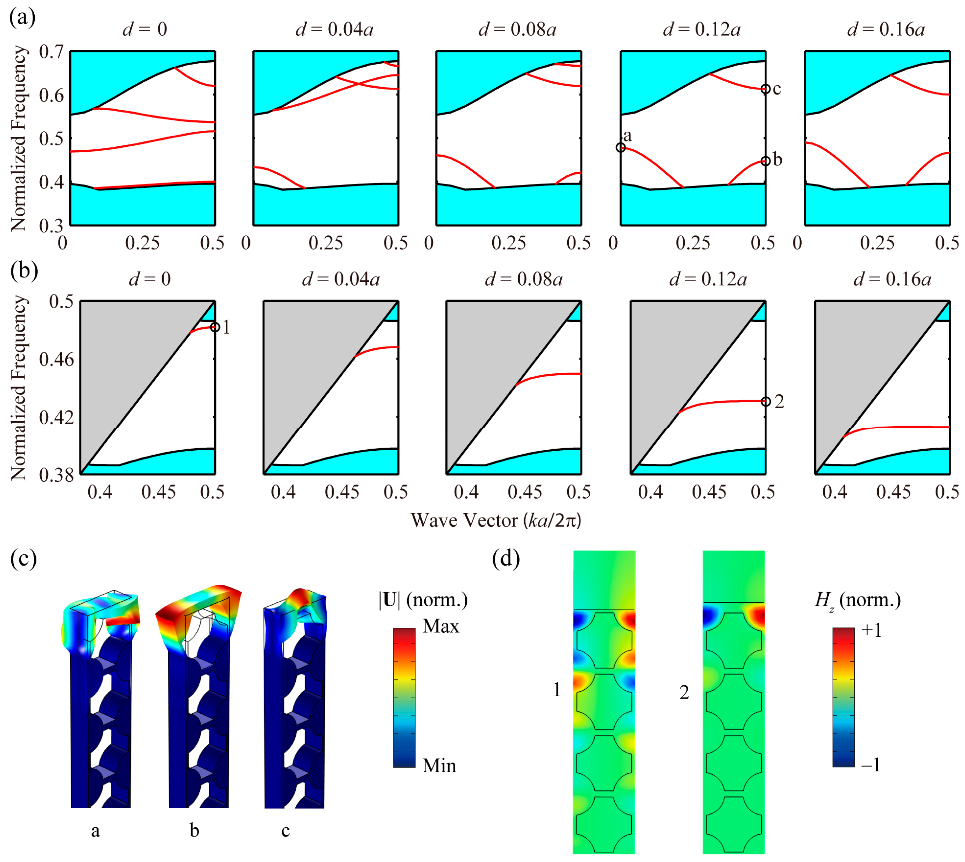
Figure 5.
Dispersion curves of the surface wave bands of phononic (a) and photonic even (b) modes for different τ, where τ increases from 0.05 to 0.2 with a step of 0.05. The cyan and gray areas represent the projected bulk modes and light cone, respectively. (c) Displacement field distributions and deformed patterns corresponding to different phononic surface bands. (d) Magnetic field (HZ) distributions at plane z = 0, corresponding to different photonic surface bands.
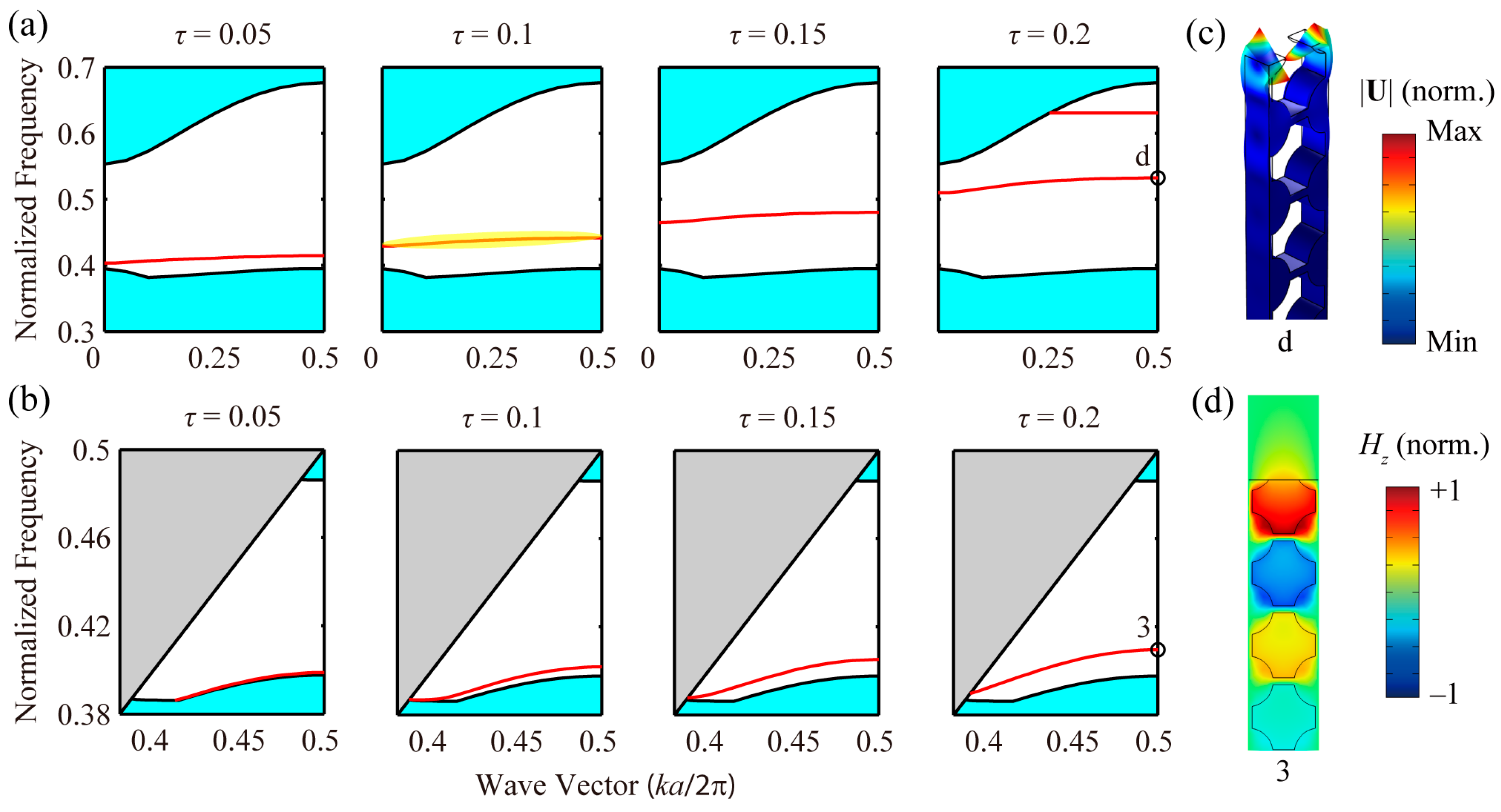
Figure 6.
Variations of the group velocity and group velocity dispersion (GVD) with the frequency for the surface acoustic waves (SAW) band marked with yellow color in Figure 5a. Blue and red lines denote the group index and the GVD, respectively.
Figure 6.
Variations of the group velocity and group velocity dispersion (GVD) with the frequency for the surface acoustic waves (SAW) band marked with yellow color in Figure 5a. Blue and red lines denote the group index and the GVD, respectively.

Figure 7.
Dispersion curves of the surface wave bands of phononic (a) and photonic even (b) modes for different τ, where τ increases from 0.8 to 0.9 with a step of 0.05. The cyan and gray areas represent the projected bulk modes and light cone, respectively.
Figure 7.
Dispersion curves of the surface wave bands of phononic (a) and photonic even (b) modes for different τ, where τ increases from 0.8 to 0.9 with a step of 0.05. The cyan and gray areas represent the projected bulk modes and light cone, respectively.

Figure 8.
Variations of the group velocity and GVD with the frequency for the surface optical waves (SOW) band marked with yellow color in Figure 7b. Blue and red lines denote the group index and the GVD, respectively.
Figure 8.
Variations of the group velocity and GVD with the frequency for the surface optical waves (SOW) band marked with yellow color in Figure 7b. Blue and red lines denote the group index and the GVD, respectively.

Figure 9.
Dispersion curves of the surface wave bands of phononic (a) and photonic odd (b) modes for different d, where d increases from 0 to 0.16a with a step of 0.04a. The cyan and gray areas represent the projected bulk modes and light cone, respectively. (c) Displacement field distributions and deformed patterns corresponding to different phononic surface bands. (d) Electric field (EZ) distributions at plane z = 0 corresponding to different photonic surface bands.
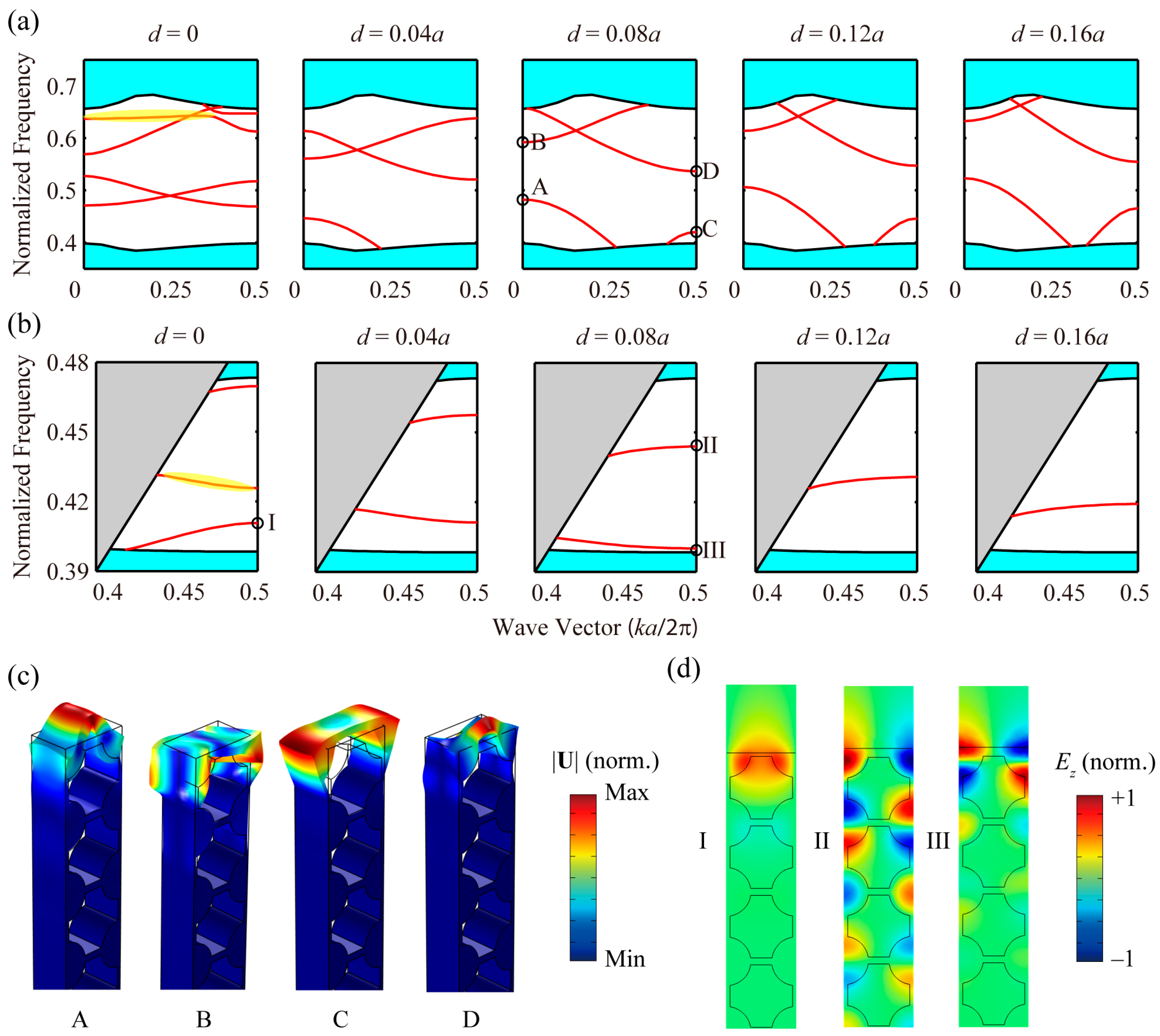
Figure 10.
Variations of the group velocity and GVD with the frequency for the SAW (a) and SOW (b) bands marked with yellow color in Figure 9. Blue and red lines denote the group index and the GVD, respectively.
Figure 10.
Variations of the group velocity and GVD with the frequency for the SAW (a) and SOW (b) bands marked with yellow color in Figure 9. Blue and red lines denote the group index and the GVD, respectively.

Figure 11.
Dispersion curves of the surface wave bands of phononic (a) and photonic odd (b) modes for different τ, where τ increases from 0.05 to 0.2 with a step of 0.05. The cyan and gray areas represent the projected bulk modes and light cone, respectively. (c) Displacement field distributions and deformed patterns corresponding to different phononic surface bands. (d) Electric field (EZ) distributions at plane z = 0 corresponding to different photonic surface bands.

Figure 12.
Dispersion curves of the surface wave bands of phononic (a) and photonic odd (b) modes for different τ, where τ increases from 0.8 to 0.9 with a step of 0.05. The cyan and gray areas represent the projected bulk modes and light cone, respectively.
Figure 12.
Dispersion curves of the surface wave bands of phononic (a) and photonic odd (b) modes for different τ, where τ increases from 0.8 to 0.9 with a step of 0.05. The cyan and gray areas represent the projected bulk modes and light cone, respectively.
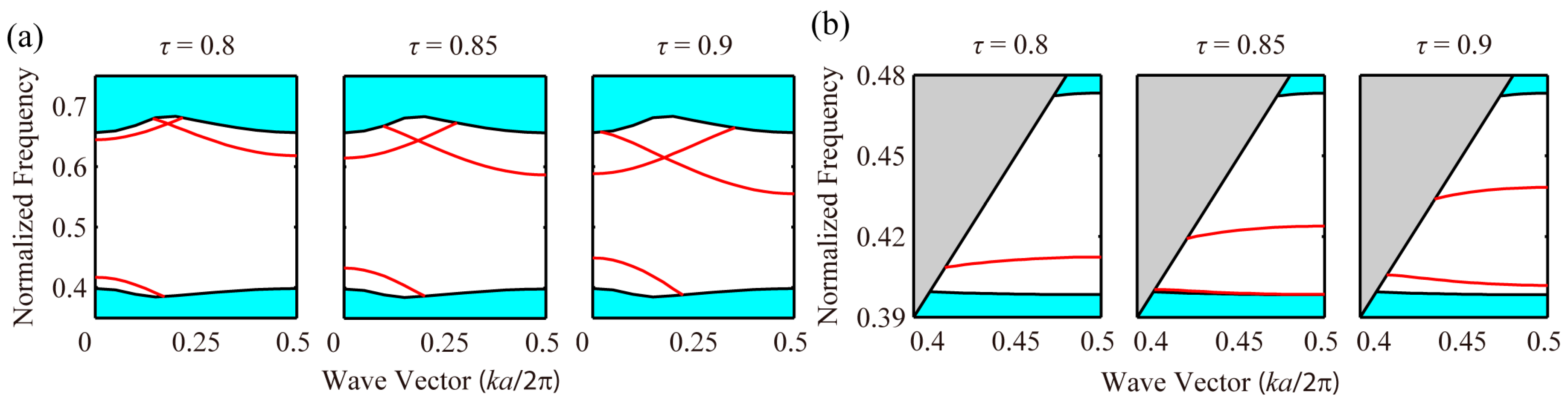
Figure 13.
Dispersion curves of the surface wave bands of photonic odd mode, where the geometrical parameters are r = 0.35a, w = 0.9a, t = 0.4a, d = 0.04a (a), and τ = 0.2 (b), respectively. The cyan and gray areas represent the projected bulk modes and light cone, respectively. (c) Electric field (EZ) distributions at plane z = 0 corresponding to different photonic surface bands.

© 2017 by the authors. Licensee MDPI, Basel, Switzerland. This article is an open access article distributed under the terms and conditions of the Creative Commons Attribution (CC BY) license (http://creativecommons.org/licenses/by/4.0/).
Share and Cite
MDPI and ACS Style
Ma, T.-X.; Wang, Y.-S.; Zhang, C. Simultaneous Guidance of Surface Acoustic and Surface Optical Waves in Phoxonic Crystal Slabs. Crystals 2017, 7, 350. https://doi.org/10.3390/cryst7110350
AMA Style
Ma T-X, Wang Y-S, Zhang C. Simultaneous Guidance of Surface Acoustic and Surface Optical Waves in Phoxonic Crystal Slabs. Crystals. 2017; 7(11):350. https://doi.org/10.3390/cryst7110350
Chicago/Turabian StyleMa, Tian-Xue, Yue-Sheng Wang, and Chuanzeng Zhang. 2017. "Simultaneous Guidance of Surface Acoustic and Surface Optical Waves in Phoxonic Crystal Slabs" Crystals 7, no. 11: 350. https://doi.org/10.3390/cryst7110350
Note that from the first issue of 2016, this journal uses article numbers instead of page numbers. See further details here.