Article

Unexpected Au Alloying in Tailoring In-Doped SnTe Nanostructures with Gold Nanoparticles

School of Physics and Astronomy, University of Leeds, Leeds LS2 9JT, UK
*
Author to whom correspondence should be addressed.
Crystals 2017, 7(3), 78; https://doi.org/10.3390/cryst7030078
Submission received: 27 December 2016 / Revised: 28 February 2017 / Accepted: 1 March 2017 / Published: 6 March 2017
(This article belongs to the Special Issue Topological Crystalline Insulators: Current Progress and Prospects)

Abstract

:
Materials with strong spin-orbit interaction and superconductivity are candidates for topological superconductors that may host Majorana fermions (MFs) at the edges/surfaces/vortex cores. Bulk-superconducting carrier-doped topological crystalline insulator, indium-doped tin telluride (In-SnTe) is one of the promising materials. Robust superconductivity of In-SnTe nanostructures has been demonstrated recently. Intriguingly, not only 3-dimensional (3D) nanostructures but also ultra-thin quasi-2D and quasi-1D systems can be grown by the vapor transport method. In particular, nanostructures with a controlled dimension will give us a chance to understand the dimensionality and the quantum confinement effects on the superconductivity of the In-SnTe and may help us work on braiding MFs in various dimensional systems for future topological quantum computation technology. With this in mind, we employed gold nanoparticles (GNPs) with well-identified sizes to tailor In-SnTe nanostructures grown by vapor transport. However, we could not see clear evidence that the presence of the GNPs is necessary or sufficient to control the size of the nanostructures. Nevertheless, it should be noted that a weak correlation between the diameter of GNPs and the dimensions of the smallest nanostructures has been found so far. To our surprise, the ones grown under the vapor–liquid–solid mechanism, with the use of the GNPs, contained gold that is widely and inhomogeneously distributed over the whole body.

1. Introduction

Topological insulators (TIs) are a new class of materials whose valence band has an odd property due to a band inversion between the bottom of the original conduction and the top of the original valence bands by a strong spin-orbit interaction (SOI). TI materials can be defined by their nontrivial topology that requires the existence of gapless (non-insulating thereby metallic) edge/surface states inside a band gap originated from bulk states. In addition, time reversal symmetry and inversion symmetry in the crystal protect the gapless states of TIs [1,2,3]. Similarly, the gapless states are topologically protected by mirror symmetries of the crystalline structure in topological crystalline insulators (TCIs), a member of the TI family [4].
Tin telluride (SnTe) is a narrow-gap semiconductor and one of the first materials experimentally recognized as an existing TCI [5,6]. Hole-doped SnTe can superconduct by self doping (i.e., Sn vacancy) [7] or chemical doping [8,9,10]. Indium-doped tin telluride (In-SnTe) is known as a hole-doped semiconductor from normal charge balance rules based on the number of valence electrons in Sn 2 + , In 1 + , and Te 2 . However, an actual carrier concentration of In-SnTe seems to be determined in a slightly more complicated way due to the valence-skip nature of In (i.e., In 1 + and In 3 + ) [9,11]. Nevertheless, superconducting In-SnTe has been attracting a lot of attention [9,11,12,13,14,15] because superconducting doped topological materials are candidates for topological superconductors [16,17,18,19,20,21,22,23] that can harbor Majorana fermions [24,25]. Moreover, its robust superconductivity and simple sample handling [15,26] are a great advantage compared with other superconducting doped TIs [27,28,29,30].
Soon after the discovery of SnTe a bulk TCI, several methods to grow SnTe nanostructures by vapor transport with Ar gas flow with/without a gold catalyst were reported [31,32,33,34,35,36]. These suggested that In-SnTe nanostructures can be made available with similar growth methods. In fact, several groups have recently investigated the properties of In-SnTe nanostructures grown by the vapor transport growth (VTG) methods with/without Ar gas flow [26,37]. Furthermore, robust bulk superconductivity of In-SnTe nanoplates/nanoflakes have been reported [26], which has opened the door to fabricate advanced superconducting devices using In-SnTe nanostructures.
More recently, we have successfully grown In-SnTe nanorods/nanowires without a gold catalyst by a very similar VTG method reported in Ref. [26] and at a relatively higher temperature than that of the VTG with Ar gas flow [31,32,33,34,35,37]. However, the actual dimensions of In-SnTe nanorods/nanowires grown without any catalyst materials on a Si/SiO 2 substrate in an evacuated quartz glass tube are often too thick to be a one-dimensional object with a single conduction channel. It is of importance to deepen our understanding of the dimensionality and the quantum confinement effects on the superconductivity of In-SnTe, or more generally, the superconductivity with a strong SOI. Therefore it is necessary to be able to control the dimensions of the nanostructures with respect to the exciton Bohr radius of bulk In-SnTe which can be similar to that of bulk SnTe (95 nm) [38]. Motivated by a report that there is a correlation between the width of nanowires and size of gold-SnTe alloy particles [33], we have investigated the possibility of restricting the dimensions of nanowires using gold nanoparticles (GNPs) assuming that gold (Au) will work as a catalyst under the vapor–liquid–solid (V–L–S) growth mechanism in our high-temperature VTG method, which turns out to be not so simple.

2. Results and Discussions

In-SnTe nanostructures can be grown without an Au catalyst by the VTG method (see Figure 1a,b). In this method, the growth mechanism is a vapor–solid (V–S) growth, in which clean and pure In-SnTe nanoplates/flakes and/or nanorods/nanowires can be grown irrespective of substrate materials. However, it is hard to control the actual dimensions of In-SnTe nanostructures grown by the VTG method without GNPs through manipulation of only three parameters; temperature at a source material, temperature gradient, and growth time.
We investigated the possibility to control the dimensions of nanostructures by the use of various diameters of GNPs in our high-temperature VTG method. In this report, we will focus on the results from the use of 20- and 50-nm GNPs. It should be noted that a similar correlation between the diameter of GNPs and the dimensions of the smallest nanostructures was found in this work. For example, a nanoneedle shown in Figure 1e is one of the smallest nanostructures grown by the use of 20-nm GNPs. However, nanostructures as small as that shown in Figure 1e could not be observed among samples grown either by the use of 50-nm GNPs (e.g., Figure 1c,d) or without GNPs (e.g., Figure 1a,b). Obviously, further statistical studies are necessary in order to quantify the size effect of GNPs on the control of the dimensions of In-SnTe nanostructures.
In order to demonstrate that the GNPs will help In-SnTe nanostructures nucleate and work as a gold catalyst in our VTG method, we first confirmed that the GNPs are in liquid phase at the temperature (∼610 C) for our VTG. After In-SnTe vapor transports from a chunk of polycrystalline source inside a sealed evacuated quartz glass tube, many In-SnTe nanostructures were observed at the place where the GNPs were originally located on a silicon substrate. Energy dispersive X-ray (EDX) spectroscopy elemental mappings of In-SnTe nanostructures grown under the V–L–S mechanism with the GNPs were used to confirm that the GNPs can work as a catalyst or an impurity by measuring four elements (Sn, In, Te, and Au) over the whole area of several samples.

2.1. Preparation of Dispersedly-Deposited Gold Nanoparticles on Substrates

We used GNPs with well-identified diameters to increase the efficiency of our investigations if the GNP can work as a catalyst for supporting the growth of In-SnTe nanostructures in our high-temperature VTG method. The initial concentration of citrate-stabilized gold colloidal solutions for the nominally 20- and 50-nm GNPs were 7 × 10 11 and 4.5 × 10 10 particles/mL, respectively. In order to control the density of deposited GNPs on a substrate, we carefully diluted the colloidal solutions down to 1 × 10 9 10 6 particles/mL by pure water (MilliQ). The citrate-stabilized gold colloids exist in a negatively ionized state at a neutral pH. When increasing the concentration of positive ions (e.g., hydronium cations) by adding an acid, the concentration of neutralized gold colloids which are in equilibrium with bare GNPs increases. Therefore, the GNPs can be deposited at the surface of substrates by the van der Waals force [39,40].
A scanning electron microscope (SEM) topography of hexagonally-faceted ∼50-nm GNP dispersed on a silicon substrate (for details on the method, see Materials and Methods) is shown in Figure 2a. The shape of 50-nm GNPs on the substrate heated at 610 C in a sealed evacuated quartz glass tube for 10 min (a typical VTG time) became rounded as shown in Figure 2b. This disappearance of initial facets indicates that the GNPs melted and were liquid at high temperatures of at least at 610 C. It is reasonable that the diameter of rounded GNPs becomes smaller than that of faceted ones (See Figure 2b,c) due to the surface tension when they were liquid and polycrystalline solidification when cooling.

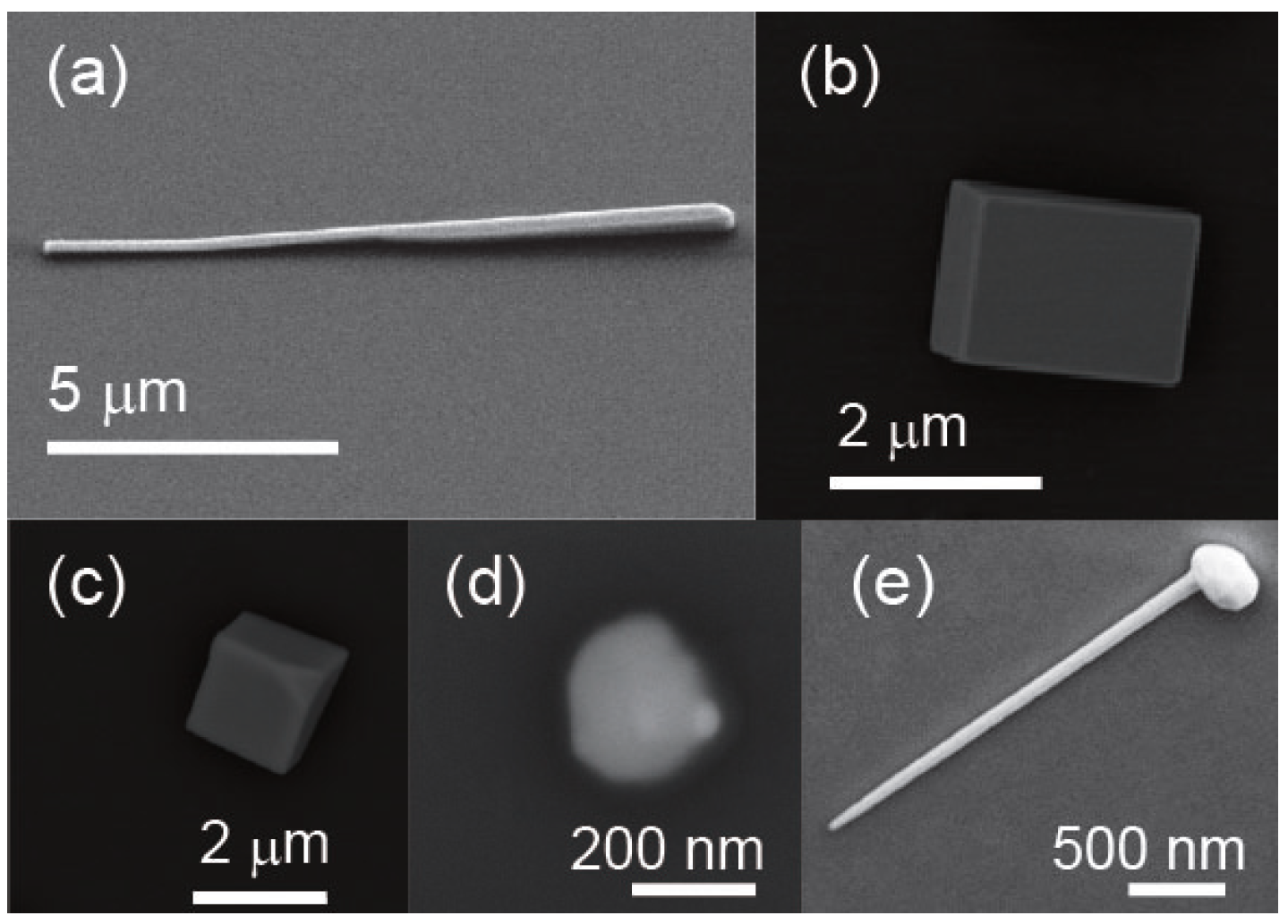
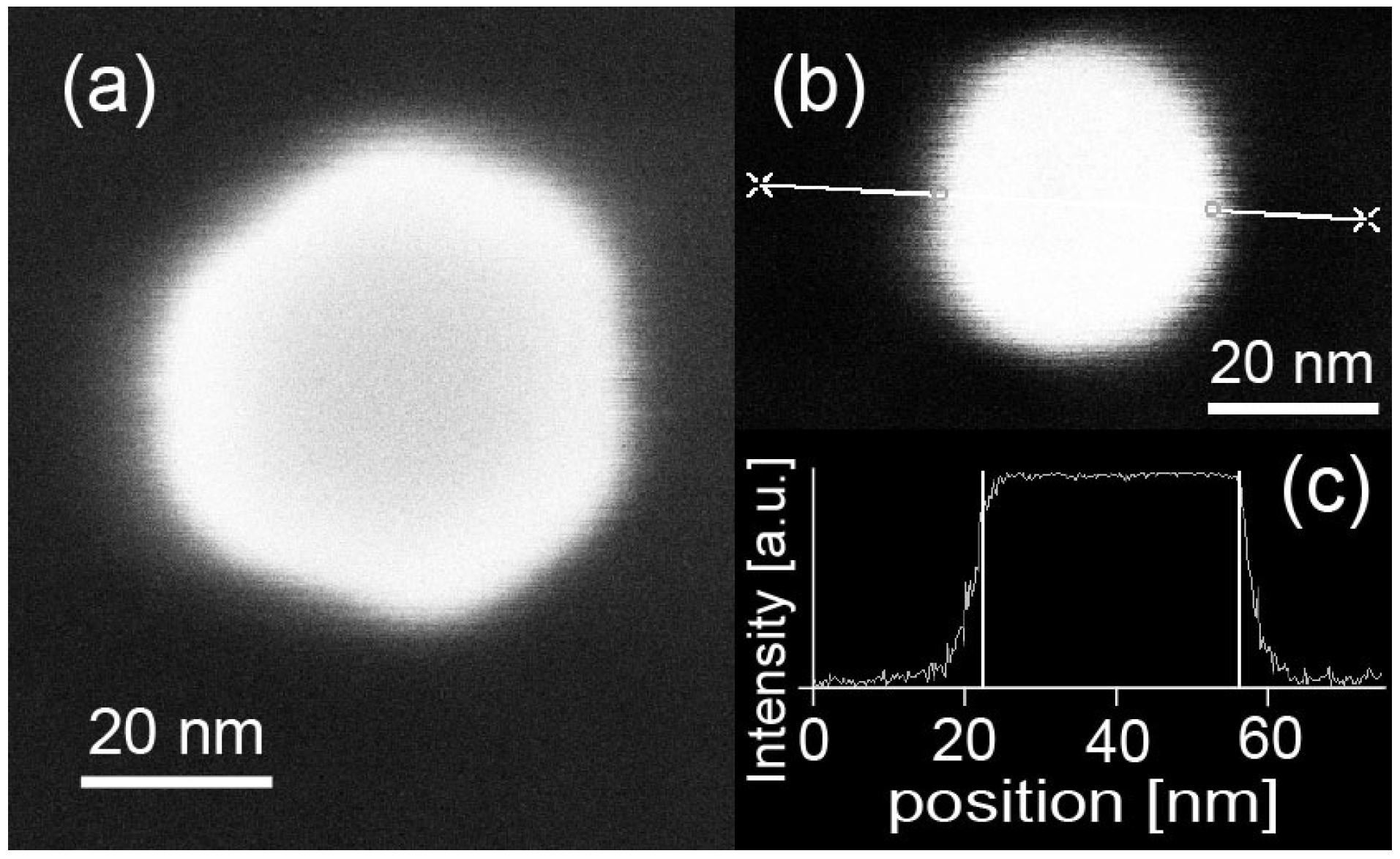
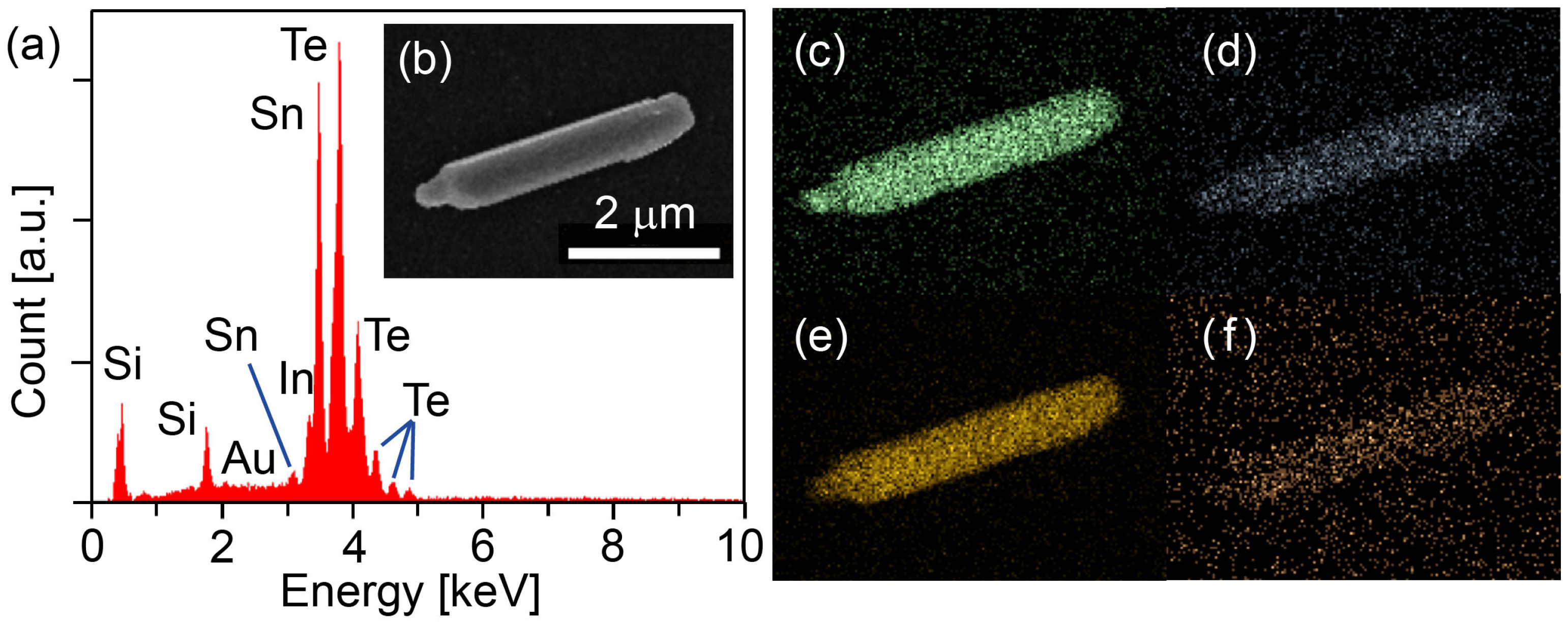
2.2. In-SnTe Nanostructures Grown under the V–L–S Mechanism with the Use of Gold Nanoparticles

Figure 3a shows EDX spectra taken from a point analysis at the middle of one of the typical In-SnTe nanostructures (nanorod) grown under the V–L–S mechanism with the use of 20-nm GNPs on a silicon substrate. The inset (Figure 3b) in Figure 3a presents a SEM topography of the nanorod sample. EDX elemental analyses with respect to Sn, In, Te, and Au for the same sample in Figure 3b are mapped in Figure 3c–f, respectively. The amount of Au estimated from the volume of a ∼20-nm GNP and that of the sample is the order of at most 0.1 atomic percent (at. % or at%), which is consistent with an expected detection limit of EDX spectroscopy. The observation of a tiny Au peak in Figure 3a and Figure S1a in the Supplementary Materials indicate the fact that the amount of one ∼20-nm GNP is detectable using our EDX.
To our surprise, the EDX elemental mappings for Au in the nanostructures (Figure 3e and Figure S2e) indicate that Au is widely spread over the whole samples in both cases. This suggests that gold in liquid phase at a high temperature (∼610 C) can be used as a building block of an alloy which is not an original In-SnTe nanostructure anymore. It is intriguing that Au does not behave as expected in our high-temperature VTG, though the GNPs seem to behave as a catalyst for the VTG of SnTe/In-SnTe nanostructures in other similar works to ours [31,32,33,34] where the growth temperature of ∼300–600 C was lower than that of our case.
It should be noted that Au and SnTe can form alloys below ∼500 C by the eutectic reaction indicated in the phase diagram of an Au ternary system (Au-Sn-Te), or more specifically (Au-SnTe) in Figure S3 reported in Ref. [41]. One plausible mechanism for the inclusion of Au into In-SnTe nanostructures is the eutectic reaction under a certain dynamic process. In the process, composite molecule vapors (In-SnTe, In, Sn, and/or Te) are being dissolved in Au in liquid phase where the soluble molecules are inhomogeneously concentrated near the surface of the liquid phase without effective mixing so that two different liquid phases with different composition (L 1 and L 2 represented in the phase diagram in Figure S3a [41]) can coexist within a tiny liquid drop of GNP(s). Hence, while In-SnTe crystals grow from the In-SnTe molecule-rich phase at a high temperature (∼610 C), Au solids grown in the other Au-rich phase can be easily included in the defects of the crystal. Here we can safely address that the phase diagram of an Au-(In-SnTe) system with relatively tiny In concentration of less than a few at% would be very similar to that of Au-SnTe. Furthermore, it should be mentioned that there might be a danger that a small portion of Au can be included in SnTe/In-SnTe nanostructures even in a lower-temperature VTG because it is known that Au can easily form alloys with Sn whose phase diagram is rich [42]. A further investigation is required in order to have a full understanding of why the V–L–S growth mechanism can work differently below or above ∼600 C and clear evidence to conclude what the real growth dynamics of In-SnTe or Au-(In-SnTe) within a tiny droplet of Au-based composite liquid phase would be [41].

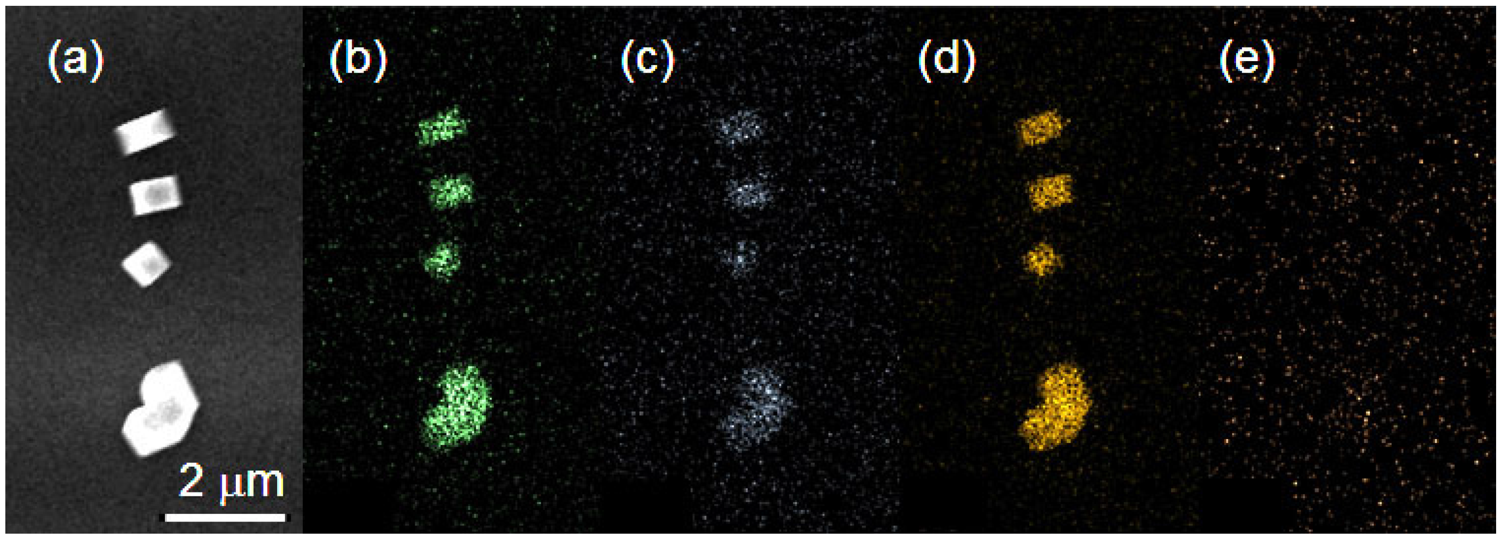
2.3. In-SnTe Nanostructures Grown under the V–S Mechanism without Gold Nanoparticles

In order to confirm the reliability of the EDX spectroscopy elemental mappings, in terms of detecting a tiny amount of Au, mappings with respect to Sn, In, Te, and Au for In-SnTe nanostructures grown under the V-S mechanism by our high-temperature VTG method without GNPs were taken (see Figure 4). Clear evidence that there is no Au in the bodies of the samples and that they are purely In-SnTe nanostructures is shown in Figure 4. Hence, we can safely conclude that there is the inclusion of gold in the body of In-SnTe nanostructures grown under the V–L–S mechanism with the use of GNPs in our high-temperature VTG.

3. Materials and Methods

In this study, we used GNPs with a nominal diameter of 20 and 50 nm. The GNPs are citrate stabilized and suspended in water, i.e., colloidal solutions purchased from BBI Solutions OEM Limited. The initial concentration of the solutions was diluted to 1 × 10 9 10 6 particles/ml by pure water (MilliQ) accordingly. Following a procedure in the literature [39,40], 100 μ L of a colloidal solution is first applied to the substrate immediately followed by 50 μ L of HCl with a concentration of 0.03 M. After keeping the solution on the substrate for 10 s to deposit the GNPs, MilliQ was used to wash off the solution and all liquid was removed by blowing it out before it could naturally dry. Once deposited, the GNPs were stable on the substrate, even being washed with ultrasonication in acetone or isopropyl alcohol (IPA). SEM topographies of dispersedly-deposited GNPs are taken by Leo1530 Gemini field-emission-gun (FEG) SEM (Carl Zeiss, Germany) and investigated.

3.1. Bulk Polycrystalline In-SnTe Growth

High-pure elements of Sn (99.999%) from Alfa Aesar, Te (99.9999%) and In (99.99%) from PI-Kem Limited were weighed in a stoichiometric ratio and put into a quartz glass tube inside a glovebox with a N 2 atmosphere. Then the tube was taken out of the glovebox and immediately hung from a gas handling system. We flushed and pumped inside the tube with highly-pure inert Ar gas so that the evacuated quartz glass tube contains the minimum possible amount of residual oxygen gas and/or humidity before sealing, which is necessary to synthesize a clean and pure polycrystalline In-doped SnTe source for the VTG. A stoichiometric mixture of all elements was melted and kept at 1000 C for 144 h in the sealed evacuated quartz glass tube using a muffle furnace FCESNOL13/1100LHM01 (SNOL, Lithuania) with intermittent shaking to promote homogeneity of the mixture; this was followed by furnace cooling. Homogeneous polycrystalline In-doped SnTe sources were synthesized.

3.2. Growth of In-SnTe Nanostructures by Vapor Transport

Silicon substrates (typically 5 mm × 20 mm) were sonicated in acetone for a few minutes and transferred into IPA which was removed by blowing it off the substrates. A prewashed substrate and polycrystalline In-SnTe source were put side by side in a sealed evacuated quartz glass tube and heated in a muffle furnace. The position of the source was adjusted inside the quartz glass tube to heat it at around 610 C and the temperature was kept for typically 10 min. The quartz glass is located in a natural temperature gradient of 1 C/cm near the rear wall of a muffle furnace so that the temperature of the substrate is a few degrees Celsius lower than that of the source polycrystalline In-SnTe. The temperature difference is essential to nucleate and grow In-SnTe nanostructures on the substrate by vapor transport. High-quality single crystal In-SnTe nanostructures are grown under the V–S mechanism on the substrate using the very similar VTG method reported in Ref. [26]. Single crystal In-SnTe nanostructures with Au inclusion as an undesirable impurity are grown under the V–L–S mechanism with the GNPs on the substrate by our high-temperature VTG method. The substrate used for the VTG is sonicated in acetone to remove unnecessary quartz debris that cover the substrate when opening the quartz glass tube and spin-coated with polymethyl methacrylate (PMMA) to protect the surface of the nanostructures from oxidation or any kind of mechanical damage. Their optical images are taken using an optical microscope BX51M (Olympus, Japan).

3.3. SEM Topography and EDX Mapping Investigation of In-SnTe Nanostructures

SEM topographies of In-SnTe nanostructures were taken using either a scanning electron microscope Nova NanoSEM450 (FEI, USA) or Carl Zeiss Leo1530 Gemini FEG-SEM. EDX spectroscopy elemental mapping data of In-SnTe nanostructure samples were taken using a FEI Nova NanoSEM450 scanning electron microscope to identify elements contained in the nanostructures.

4. Conclusions and Outlook

We investigated one of the possible methods to control the dimensions of In-SnTe nanostructures grown by vapor transport with the use of gold nanoparticles, a candidate method for catalytic vapor transport growth of In-doped SnTe under the vapor–liquid–solid growth mechanism. Contrary to what we expected given the reports regarding the catalytic behavior of gold, it turned out to be a challenging approach. Gold was easily incorporated as an undesirable impurity in the body of In-doped SnTe nanostructures grown by our high-temperature vapor transport growth method ( > 600 C). According to a rich phase diagram of binary or ternary gold alloys with respect to Sn and SnTe, the existence of gold impurity would be suspected in In-doped SnTe nanostructures grown under the vapor–liquid–solid mechanism with the GNPs even in a low-temperature vapor-transport method. It is unfortunate that we should give up considering to use gold nanoparticles for tailoring the In-SnTe nanostructures, although there may still be a chance that nanoparticles made of other catalytic elements can control the dimensions of In-SnTe nanostructures depending on their own size. Searching for such nanoparticle materials that will not form alloys with In-SnTe will be important for our scientific studies and applications for future use.

Supplementary Materials

The following are available online at www.mdpi.com/2073-4352/7/3/78/s1, Figure S1: (Color online) Investigation of the detection limit with respect to Au in energy dispersive X-ray (EDX) spectroscopy. (a) EDX spectra taken from a point analysis of one ∼20-nm GNP isolated from others on a Si substrate. The inset is (b) scanning electron microscope (SEM) topography of a ∼20-nm GNP. Scale bar in (b) is 20 nm; Figure S2: (Color online) Investigation of the constituent elements in the In-SnTe nanostructure grown by the vapor transport growth (VTG) method on a Si substrate under the V-L-S mechanism with the use of 20-nm GNPs demonstrating a reproducibility of Au alloying shown in Figure 3 in the main article. (a) Scanning electron microscope topography of a typical nanorod sample. (b)-(e) Energy dispersive X-ray (EDX) spectroscopy elemental mappings for (b) Sn, (c) In, (d) Te, and (e) Au of the sample in (a), respectively. Scale bar in (a) is 1 μ m; Figure S3: The concentration of Au vs. temperature phase diagram of ternary gold alloys Au-Sn-Te (or more specifically, Au-SnTe) [41]. L1 and L2 indicate two different liquid phases with different compositions. It is suggested that L1 has a composition of 28 at% Au, 27 at% Sn, 45 at% Te and L1 has a composition of 80 at% Au, 18 at% Sn, 2 at% Te in Ref. [41].

Acknowledgments

We thank C. Wade, E. Dransfield, M. Vaughan, G. Krishnaswamy, and M. Ali for technical assistance and help in experiments. We thank B. Johnson for our access to Chemistry laboratory (School of Physics and Astronomy, University of Leeds) and E. Linfield for the use of equipment in Nanotechnology cleanroom (School of electronic and electrical engineering, Faculty of Engineering, University of Leeds). We acknowledge A. Kulak (School of Chemistry, University of Leeds) for taking SEM/EDX data and H. Joyce for a fruitful discussion about deposition of gold nanoparticles. This work is supported by the start up funding of the School of Physics and Astronomy, University of Leeds and an EPSRC DTA studentship.

Author Contributions

S.S. conceived and designed the experiments. S.A. and B.S. contributed equally to this work. S.S. wrote the paper.

Conflicts of Interest

The founding sponsors had no role in the design of the study; in the collection, analyses, or interpretation of data; in the writing of the manuscript, and in the decision to publish the results.

Abbreviations

The following abbreviations are used in this manuscript:
TI
topological insulator
TCI
topological crystalline insulator
TSC
topological superconductor
MF
Majorana fermion
SOI
spin-orbit interaction
In-SnTe
indium-doped tin telluride
VTG
vapor transport growth
V–L–S
vapor–liquid–solid
V–S
vapor–solid
GNP
gold nanoparticle
SEM
scanning electron microscope
FEG-SEM
field-emission-gun scanning electron microscope
EDX
energy dispersive X-ray
IPA
isopropyl alcohol
PMMA
polymethyl methacrylate

References

  1. Hasan, M.Z.; Kane, C.L. Colloquium: Topological insulators. Rev. Mod. Phys. 2010, 82, 3045–3067. [Google Scholar] [CrossRef]
  2. Qi, X.-L.; Zhang, S.-C. Topological insulators and Superconductors. Rev. Mod. Phys. 2011, 83, 1057–1110. [Google Scholar] [CrossRef]
  3. Ando, Y. Topological insulator materials. J. Phys. Soc. Jpn. 2013, 82, 102001. [Google Scholar] [CrossRef]
  4. Fu, L. Topological crystalline insulators. Phys. Rev. Lett. 2011, 106, 106802. [Google Scholar] [CrossRef] [PubMed]
  5. Hsieh, T.H.; Lin, H.; Liu, U.; Duan, W.; Bansil, A.; Fu, L. Topological crystalline insulators in SnTe material class. Nat. Commun. 2012, 3, 982. [Google Scholar] [CrossRef] [PubMed] [Green Version]
  6. Tanaka, Y.; Ren, Z.; Sato, T.; Nakayama, K.; Souma, S.; Takahashi, T.; Segawa, K.; Ando, Y. Experimental realization of a topological crystalline insulator in SnTe. Nat. Phys. 2012, 8, 800–803. [Google Scholar] [CrossRef]
  7. Hulm, J.K.; Jones, C.K.; Deis, D.W.; Fairbank, H.A.; Lawless, P.A. Superconducting interactions in tin telluride. Phys. Rev. 1968, 169, 388–394. [Google Scholar] [CrossRef]
  8. Mathur, M.P.; Deis, D.W.; Jones, C.K.; Carr, W.J., Jr. Superconductivity as a function of carrier density and magnetic spin concentration in the SnTe-MnTe system. J. Phys. Chem. Solids 1973, 34, 183–188. [Google Scholar] [CrossRef]
  9. Erickson, A.S.; Chu, J.-H.; Toney, M.F.; Geballe, T.H.; Fisher, I.R. Enhanced superconducting pairing interaction in indium-doped tin telluride. Phys. Rev. B 2009, 79, 024520. [Google Scholar] [CrossRef]
  10. Mizuguchi, Y.; Miura, O. High-pressure synthesis and Superconductivity of Ag-doped topological crystalline insulator SnTe (Sn1−xAgxTe with x = 0 − 0.5). J. Phys. Soc. Jpn. 2016, 85, 053702. [Google Scholar] [CrossRef]
  11. Haldolaarachchige, N.; Gibson, Q.; Xie, W.; Nielsen, M.B.; Kushwaha, S.; Cava, R.J. Anomalous composition dependence of the superconductivity in In-doped SnTe. Phys. Rev. B 2016, 93, 024520. [Google Scholar] [CrossRef]
  12. Balakrishnan, G.; Bawden, L.; Cavendish, S.; Lees, M.R. Superconducting properties of the In-substituted topological crystalline insulator SnTe. Phys. Rev. B 2013, 87, 140507. [Google Scholar] [CrossRef]
  13. Zhong, R.D.; Schneeloch, J.A.; Shi, X.Y.; Xu, Z.J.; Zhang, C.; Tranquada, J.M.; Li, Q.; Gu, G.D. Optimizing the superconducting transition temperature and upper critical field of Sn1−xInxTe. Phys. Rev. B 2013, 88, 020505. [Google Scholar] [CrossRef]
  14. Novak, M.; Sasaki, S.; Kriener, M.; Segqawa, K.; Ando, Y. Unusual nature of fully gapped superconductivity in In-doped SnTe. Phys. Rev. B 2013, 88, 140502. [Google Scholar] [CrossRef]
  15. Sasaki, S.; Ren, Z.; Taskin, A.A.; Segawa, K.; Fu, L.; Ando, Y. Odd-parity pairing and topological superconductivity in a strongly spin-orbit coupled semiconductor. Phys. Rev. Lett. 2012, 109, 217004. [Google Scholar] [CrossRef] [PubMed]
  16. Fu, L.; Kane, C.L. Superconducting proximity effect and Majorana fermions at the surface of a topological insulator. Phys. Rev. Lett. 2008, 100, 096407. [Google Scholar] [CrossRef] [PubMed]
  17. Sato, M.; Takahashi, Y.; Fujimoto, S. Non-abelian topological order in s-wave superfluids of ultracold fermionic atoms. Phys. Rev. Lett. 2009, 103, 020401. [Google Scholar] [CrossRef] [PubMed]
  18. Fu, L.; Berg, E. Odd-parity topological superconductors: Theory and application to CuxBi2Se3. Phys. Rev. Lett. 2010, 105, 097001. [Google Scholar] [CrossRef] [PubMed]
  19. Schnyder, A.P.; Ryu, S.; Furusaki, A.; Ludwig, A.W.W. Classification of topological insulators and superconductors in three spatial dimensions. Phys. Rev. B 2008, 78, 195125. [Google Scholar] [CrossRef]
  20. Ando, Y.; Fu, L. Topological crystalline insulators and topological superconductors: From concepts to materials. Annu. Rev. Condens. Matter Phys. 2015, 6, 361–381. [Google Scholar] [CrossRef]
  21. Beenakker, C.; Kouwenhoven, L. A road to reality with topological superconductors. Nat. Phys. 2016, 12, 618–621. [Google Scholar] [CrossRef]
  22. Sasaki, S.; Mizushima, T. Superconducting doped topological materials. Physica C 2015, 514, 206–217. [Google Scholar] [CrossRef]
  23. Sato, M.; Ando, Y. Topological superconductors. arXiv 2016. [Google Scholar]
  24. Wilczek, F. Majorana returns. Nat. Phys. 2009, 5, 614–618. [Google Scholar] [CrossRef]
  25. Alicea, J. New directions in the pursuit of Majorana fermions in solid state systems. Rep. Prog. Phys. 2012, 75, 076501. [Google Scholar] [CrossRef] [PubMed]
  26. Sasaki, S.; Ando, Y. Superconducting Sn1−xInxTe Nanoplates. Cryst. Growth Des. 2015, 15, 2748–2752. [Google Scholar] [CrossRef]
  27. Hor, Y.S.; Williams, A.J.; Checkelsky, J.G.; Roushan, P.; Seo, J.; Xu, Q.; Zandbergen, H.W.; Yazdani, Q.; Ong, N.P.; Cava, R.J. Superconductivity in CuxBi2Se3 and its implications for pairing in the undoped topological insulator. Phys. Rev. Lett. 2010, 104, 057001. [Google Scholar] [CrossRef] [PubMed]
  28. Sasaki, S.; Kriener, M.; Segawa, K.; Yada, K.; Tanaka, Y.; Sato, M.; Ando, Y. Topological superconductivity in CuxBi2Se3. Phys. Rev. Lett. 2011, 107, 217001. [Google Scholar] [CrossRef] [PubMed]
  29. Kriener, M.; Segawa, K.; Sasaki, S.; Ando, Y. Anomalous suppression of the superfluid density in the CuxBi2Se3 superconductor upon progressive Cu intercalation. Phys. Rev. B 2012, 86, 180505. [Google Scholar] [CrossRef]
  30. Liu, Z.; Yao, X.; Shao, J.; Zuo, M.; Pi, L.; Tan, S.; Zhang, C.; Zhang, Y. Superconductivity with Topological Surface State in SrxBi2Se3. J. Am. Chem. Soc. 2015, 137, 10512–10515. [Google Scholar] [CrossRef] [PubMed]
  31. Saghir, M.; Lees, M.R.; York, S.J.; Balakrishnan, G. Synthesis and characterization of nanomaterials of the topological crystalline insulator SnTe. Cryst. Growth Des. 2014, 14, 2009–2013. [Google Scholar] [CrossRef]
  32. Safdar, M.; Wang, Q.; Mirza, M.; Wang, Z.; He, J. Crystal shape engineering of topological crystalline insulator SnTe microcrystals and nanowires with huge thermal activation energy Gap. Cryst. Growth Des. 2014, 14, 2502–2509. [Google Scholar] [CrossRef]
  33. Li, Z.; Shao, S.; Li, N.; McCall, K.; Wang, J.; Zhang, S.X. Single crystalline nanostructures of topological crystalline insulator SnTe with distinct facets and morphologies. Nano Lett. 2013, 13, 5443–5448. [Google Scholar] [CrossRef] [PubMed]
  34. Shen, J.; Jung, Y.; Disa, A.S.; Walker, F.J.; Ahn, C.H.; Cha, J.J. Synthesis of SnTe nanoplates with {100} and {111} surfaces. Nano Lett. 2014, 14, 4183–4188. [Google Scholar] [CrossRef] [PubMed]
  35. Safdar, M.; Wang, Q.; Mirza, M.; Wang, Z.; Xu, K.; He, J. Topological Surface Transport Properties of Single-Crystalline SnTe Nanowire. Nano Lett. 2013, 13, 5344–5349. [Google Scholar] [CrossRef] [PubMed]
  36. Wang, Q.; Wang, F.; Li, J.; Wang, Z.; Zhan, X.; He, J. Low-dimensional topological crystalline insulators. Small 2015, 11, 4613–4624. [Google Scholar] [CrossRef] [PubMed]
  37. Shen, J.; Xie, Y.; Cha, J.J. Revealing surface states in In-doped SnTe Nanoplates with low bulk mobility. Nano Lett. 2015, 15, 3827–3832. [Google Scholar] [CrossRef] [PubMed]
  38. Guo, S.; Fidler, A.F.; He, K.; Su, D.; Chen, G.; Lin, Q.; Pietryga, J.M.; Klimov, V.I. Shape-controlled narrow-gap SnTe nanostructures: From nanocubes to nanorods and nanowires. J. Am. Chem. Soc. 2015, 137, 15074–15077. [Google Scholar] [CrossRef] [PubMed]
  39. Woodruff, H.J.; Ratchford, J.B.; Goldthorpe, I.A.; McIntyre, P.C.; Chidsey, C.E.D. Vertically oriented germanium nanowires grown from gold Colloids on silicon substrates and subsequent gold removal. Nano Lett. 2007, 7, 1637–1642. [Google Scholar] [CrossRef] [PubMed]
  40. Joyce, J.H.; Gao, Q.; Tan, H.H.; Jagadish, C.; Kim, Y.; Zou, J.; Smith, L.M.; Jackson, H.E.; Yarrison-Rice, J.M.; Parkinson, P.; et al. III–V semiconductor nanowires for optoelectronic device applications. Prog. Quantum Electron. 2011, 35, 23–75. [Google Scholar] [CrossRef]
  41. Prince, A.; Raynor, G.V.; Evans, D.S. Ternary systems Au-Sn-Te. In Phase Diagram of Ternary Gold Alloys; The Institute of Metals: London, UK, 1990; pp. 456–466. [Google Scholar]
  42. Okamoto, H.; Massalski, T.B. (Eds.) Phase diagram of binary gold alloys. In Binary Alloy Phase Diagrams; ASM International: Metals Park, OH, USA, 1987; p. 343.
Figure 1. Scanning electron microscope topography of In-SnTe nanostructures grown (a,b) without gold nanoparticles (GNP), (c,d) with the use of 50-nm GNPs, and (e) with the use of 20-nm GNPs on a silicon substrate by the very similar VTG method reported in [26]. Scale bar for (a), (b,c), (d), and (e) are 5 μ m, 2 μ m, 200 nm, and 500 nm, respectively.
Crystals 07 00078 g001
Figure 2. Scanning electron microscope topography of (a) a typical 50-nm GNP dispersed from the gold colloidal solution on a Si substrate before heating and (b) one of the same GNPs after heating at 610 C. (c) Line profile of the intensity of secondary electrons in (b). Scale bar in (b,c) is 20 nm.
Crystals 07 00078 g002
Figure 3. (Color online) Investigation of the constituent elements in the indium-doped tin telluride (In-SnTe) nanostructures grown by the vapor transport growth (VTG) method on a Si substrate under the vapor-liquid-solid (V–L–S) mechanism with the use of 20-nm GNPs. (b) Scanning electron microscope (SEM) topography of a typical nanorod on a Si substrate. (a) Energy dispersive X-ray (EDX) spectra taken from a point analysis in the middle of the sample in (b). (cf) EDX spectroscopy elemental mappings for (c) Sn, (d) In, (e) Te, and (f) Au of the sample in (b), respectively. Scale bar in (b) is 2 μ m.
Crystals 07 00078 g003
Figure 4. (Color online) Investigation of the constituent elements in the In-SnTe nanostructures grown by vapor transport on a Si substrate under the vapor-solid (V–S) mechanism without GNPs and energy dispersive X-ray (EDX) spectroscopy mapping of In-SnTe nanostructures grown under the V–S mechanism without GNPs. (a) SEM topography. (be) EDX spectroscopy elemental mappings for (b) Sn, (c) In, (d) Te, and (e) Au of the nanostructures in (a). Scale bar in (a) is 2 μ m.
Crystals 07 00078 g004

