One Step Preparation of Fe–FeO–Graphene Nanocomposite through Pulsed Wire Discharge
by
 , and
, and
Xin Gao
1 ,
,
Naoaki Yokota
2,
Hayato Oda
2,
Shigeru Tanaka
2,
Kazuyuki Hokamoto
2 and
Pengwan Chen
1,* 1
State Key Laboratory of Explosion Science and Technology, Beijing Institute of Technology, Beijing 100081, China
2
Institute of Pulsed Power Science, Kumamoto University, Kumamoto 860-8555, Japan
*
Author to whom correspondence should be addressed.
Crystals 2018, 8(2), 104; https://doi.org/10.3390/cryst8020104
Submission received: 31 January 2018
/
Revised: 14 February 2018
/
Accepted: 14 February 2018
/
Published: 23 February 2018
(This article belongs to the Special Issue Graphene Mechanics)
Abstract
:The Fe–FeO–graphene nanocomposite material was produced successfully by pulsed wire discharge in graphene oxide (GO) suspension. Pure iron wires with a diameter of 0.25 mm and a length of 100 mm were used in the experiments. The discharge current and voltage were recorded to analyze the process of the pulsed wire discharge. The as-prepared samples—under different charging voltages—were recovered and characterized by X-ray diffraction (XRD), scanning electron microscopy (SEM), Raman spectroscopy, and transmission electron microscopy (TEM). Curved and loose graphene films that were anchored with spherical Fe and FeO nanoparticles were obtained at the charging voltage of 8–10 kV. The present study discusses the mechanism by which the Fe–FeO–graphene nanocomposite material was formed during the pulsed wire discharge process.
1. Introduction
Graphene—a two-dimensional structure of carbon atoms in a hexagonal honeycomb lattice—was obtained in 2004 by Novoselov et al. [1] through exfoliating the highly oriented pyrolytic graphite with a tape, revealing the strong ambipolar electric field effect of graphene. Geim et al. [2] pointed out the immediate application of graphene in composite materials. The first graphene composite (graphene–polystyrene) was synthesized in 2006 by Stankovich et al. [3]. Thereafter, various graphene-based composite materials have been produced, i.e., graphene–polymer composite materials [3,4] and metal or metal oxide–graphene composite materials (i.e., nano Ni–graphene composite materials and nano SnO2–graphene composite material) [5,6]. Due to their excellent properties, graphene-based composite materials have been successfully utilized in electronic and optoelectronic devices, chemical sensors, and energy storage [7].
Nanoscale iron and iron oxide materials have demonstrated various excellent properties, including large specific surface area, high reactivity, and strong reducibility. In addition, they have been extensively applied for pollutants degradation, i.e., chlorohydrocarbon, nitrobenzenes, chlorinated phenols, poly-chlorinated biphenyls, heavy metals, and various anions from water [8,9,10]. Therefore, it is economically and ecologically effective to use iron-based catalysts. Besides, nano iron and iron oxide powders have a great potential in biomedical applications [11] for economic and ecological expedience. However, nanoparticles spontaneously tend to form microscale agglomerates, therefore, affecting the properties of nanoparticles. In graphene-based nanocomposites, the agglomeration of nanoparticles can be inhibited through anchoring nanoparticles on the surface of graphene nanosheets [6]. Composite materials have demonstrated excellent properties in high energy storage and efficient catalysis due to their large specific surface. Because of their promising applications, Fe–FeO–graphene nanocomposite materials have become a hot spot research area [12,13].
Pulsed wire discharge, also known as electrical wire explosion, which occurs in vacuum or a certain media, is a phenomenon in which, the wire is evaporated in burst and bright flash by joule heating. This is conducted under the effect of a high-density current, which is produced by the discharge of a capacitor passing through a wire [14]. Then a mixture of the produced vapour and drops scatters out with a shockwave. Meanwhile, the generated vapour and drops cool down in the surrounding atmosphere to form nanoparticles. The pulsed wire discharge method has been successfully utilized to produce various nanomaterials, including metal and metal compound nanopowders, nanocomposite materials, and multiple carbon nanomaterials. Zhou et al. [15] produced copper nanoparticles by exploding copper wires in distilled water. Wada et al. [16] synthesized nano TiO2 powder by exploding Ti wire in various media. Abdelkader et al. [17] synthesized various metal carbide nanoparticles by using pulsed wire discharge in organic liquid. He et al. [18] synthesized boron nitride nanosheet/nanotube–iron nanocomposites by pulsed discharge of pure iron wire coated by boron nitride powders. Furthermore, electrical explosion of carbon fibers was used to synthesize fullerene [19,20] and carbon nanotubes [21,22]. More recently, graphene materials were obtained by electrical explosion of graphite sticks in distilled water [23]. Furthermore, several graphene-based nanocomposite materials with certain outstanding properties were synthesized via the pulsed wire discharge method [24,25]. However, in these studies, the formation mechanism of these composite materials has not been studied. In the current paper, Fe–FeO–graphene nanocomposite material was produced by exploding an iron wire in graphene oxide (GO) suspension. In addition, the mechanism of formation of Fe–FeO–graphene nanocomposite was investigated based on the analysis of the discharge current and voltage, as well as the characterization results.
2. Materials and Methods
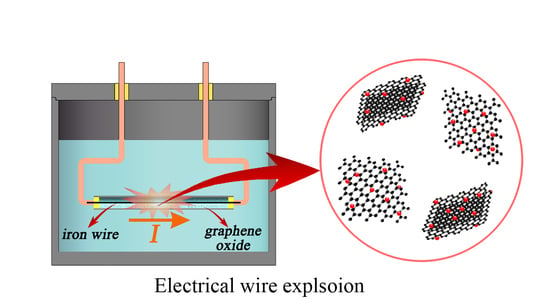
The pulsed wire discharge system consists of a rechargeable power supply, a capacitor with a capacitance of 12.5 μF, and a pulsed wire discharge chamber. The charging voltage of the system can be adjusted in the range of 0–40 kV. To recover the product of pulsed wire discharge, pulsed wire discharge tests were conducted in a cylindrical stainless-steel pulsed discharge chamber (Figure 1). An iron wire with a diameter of 0.25 mm, a length of 100 mm, and a purity of 99.9% was fixed in a plastic pipe with an inner diameter of 8 mm and a length of 100 mm. The utilized GO suspension (1 g/L) was purchased from NiSiNa materials Co and consisted of GO nanosheets and distilled water. The pipe is filled with GO suspension and was blocked by two insulation blocks. Then, the iron wire was connected to two electrodes in the cylindrical chamber and immersed in distilled water. The electrodes were connected to the capacitor for discharge. Following the pulsed discharge, the black suspension was recovered and dried in vacuum. The recovered and dried samples were kept for further characterizations. For all experiments, the current and voltage were recorded during the electrical discharge.
The phase compositions of the recovered samples were determined by X-ray diffraction (XRD) (Rigaku D/MAX-2500) using Cu Kα radiation at 40 kV work voltage and 200 mA work current at a 2θ range of 10–80°. Transmission electron microscopy (TEM) images of the products were taken by Philips Tecnai F20 S-Twin. Scanning electron microscopy (SEM) observations were taken by Hitachi S-4800. The chemical composition and bonding states of the products were probed by X-ray photoelectron spectroscopy (XPS) on a ESCALAB 250 Xi (Thermo Fisher Scientific, Waltham, MA, USA) using monochromatic AlK (1486.6 eV) X-ray sources with 30 eV pass energy in 0.05 eV step.
3. Results and Discussion
The experimental conditions of pulsed iron wire discharge are listed in Table 1, including the charging voltage and the energy stored in the capacitor. Three charging voltages (8, 10 and 20 kV) were selected.
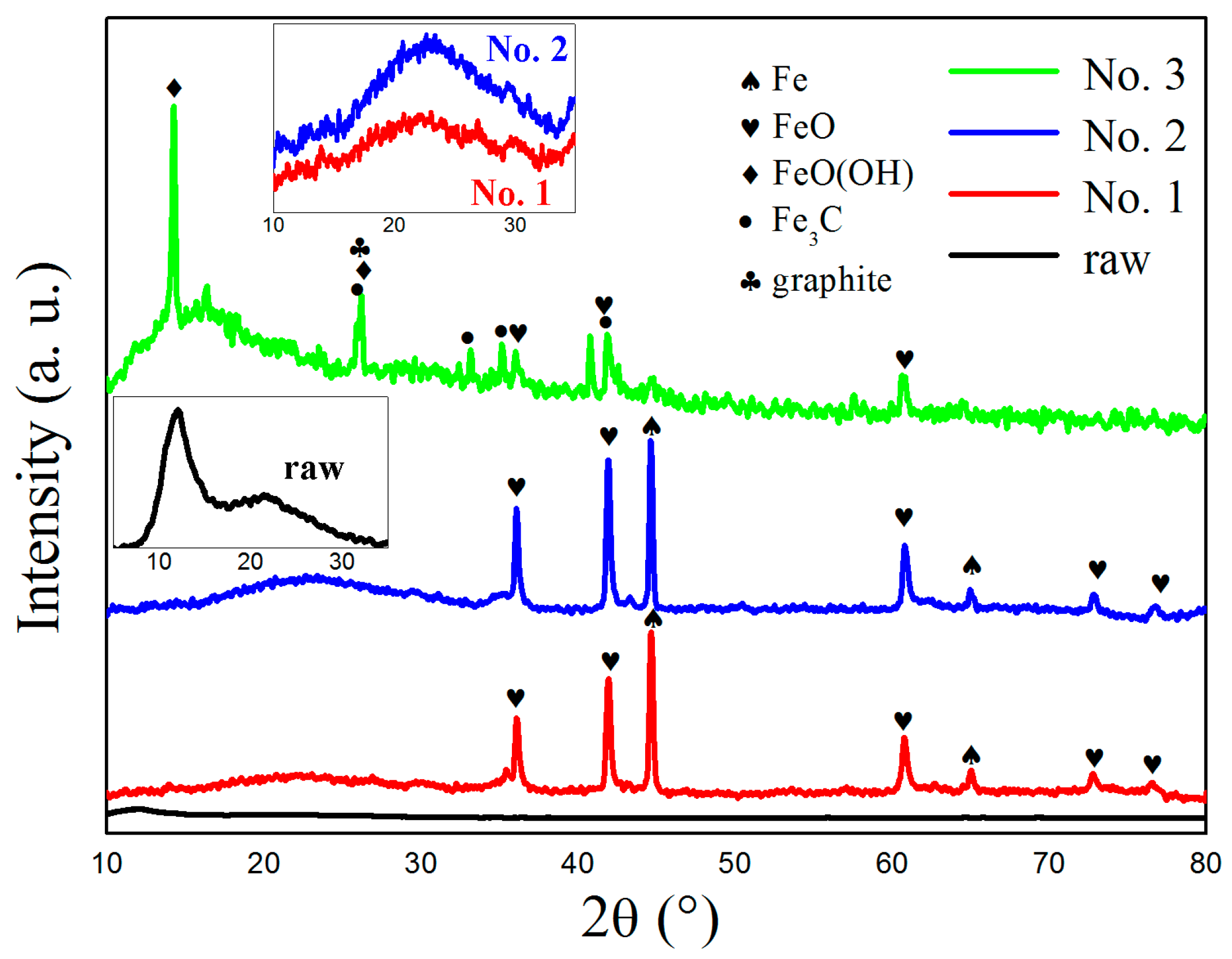
The (XRD) patterns of raw GO and the recovered samples are shown in Figure 2. The XRD pattern of raw GO (the inset of Figure 2) showed two weak and broad peaks at approximately 9–15° and 15–30°, respectively, which are assigned to the typical XRD peaks of GO [26,27,28]. The peak at 9–15° may imply agglomeration of GO sheets during the drying process. The weaker and broader peak, which appeared at 15–30°, revealed the ultra-thin structure of GO with very few graphitic layers. The broad peaks, which appeared at 20–30° in the XRD patterns of samples No. 1 and 2, also revealed the presence of graphene sheets in these samples. Besides, typical peaks of Fe and FeO were observed in all three samples. The proposed formation mechanism of FeO was referred to the reaction between H2O and iron droplets and vapour. However, the XRD pattern of sample No. 3 showed the presence of graphite, Fe3C, and FeO(OH). The XRD results showed that graphene maintained its structure when the reaction was performed at an appropriate charging voltage (8–10 kV for samples No. 1 and 2). When the charging voltage was increased to 20 kV, excessive input energy resulted in destroying the molecular structure of GO and the formation of graphite, Fe3C, and FeO(OH), which is discussed thereafter. Based on the adiabatic approximation method, iron and iron compound phase content of the recovered samples were calculated and listed in Table 2. It can be seen that the phase contents of the products are largely influenced by the charge voltage. Upon increasing the charging voltage, the iron content decreases, with an increase in the total content of iron compounds (FeO, α-FeO(OH), and Fe3C).
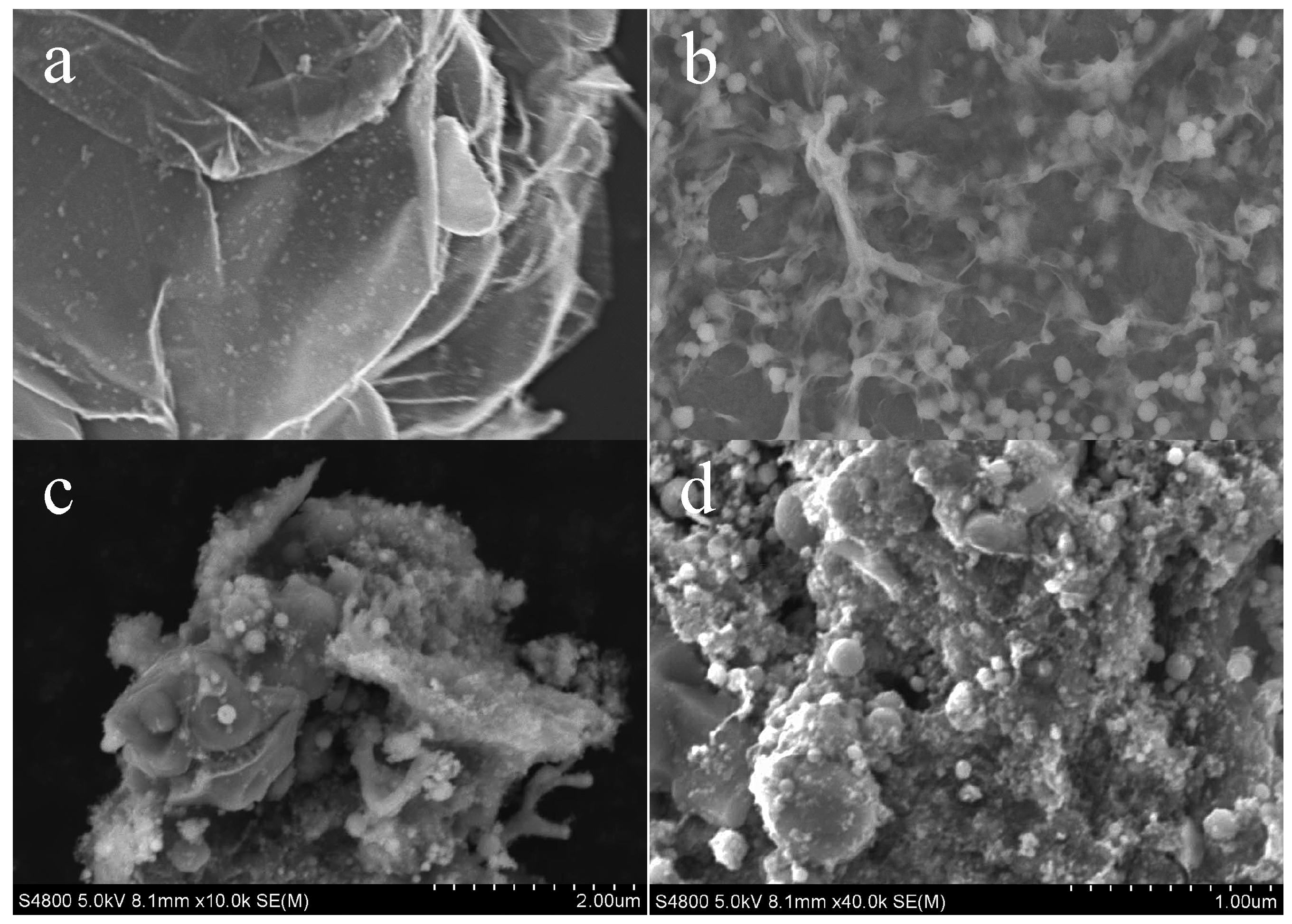
Figure 3 shows the typical SEM images of the recovered samples. At the charging voltages 8–10 kV (samples No. 1 and 2), morphology and microstructure of the recovered samples were quite similar. Figure 3a shows a typical SEM image of sample No. 1, confirming the presence of curved and loose graphene films anchored with spherical nanoparticles. Figure 3b shows a higher magnification view of Figure 3a, further confirming the presence of transparent graphene films with wrinkles, folds, and spherical nanoparticles in a size range of 50–150 nm. Similar morphology has been also reported for other graphene-based composite materials [29,30]. When the charging voltage was increased to 20 kV (sample No. 3), the microstructure and morphology of the recovered sample were quite different (Figure 3c), with the presence of irregular graphite-like microparticles and spherical nanoparticles. The higher magnification view (Figure 3d) showed the rough surface of graphite-like particles and spherical nanoparticles (50–200 nm). The spherical nanoparticles in all the recovered samples were iron or iron compound nanoparticles and the spherical shape referred to the nucleation and growth of the melted or vaporized product during the pulsed wire discharge.
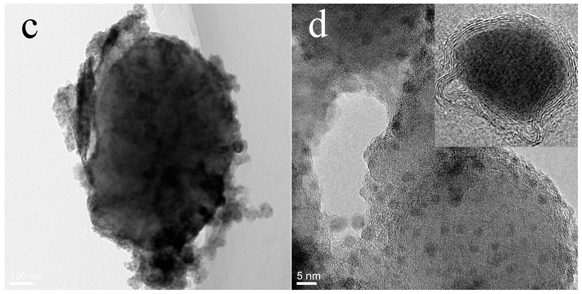
Figure 4a,b display the typical and high-resolution TEM images of sample No. 1; revealing the presence of thin extended carbon films (3–5 layers) with an inter-layer distance of approximately 0.35 nm, anchored with spherical nanoparticles (5–100 nm). Similar microstructure was also observed for other graphene-based composite materials [29,30]. The lattice distances of the spherical nanoparticles were 0.20 and 0.15 nm, which are in good agreement with those of Fe and FeO, respectively. The results confirm that the spherical nanoparticles in samples No. 1 and 2 are Fe and FeO. Figure 4c,d shows typical TEM and high-resolution TEM images of sample No. 3. Irregular graphite particles, amorphous carbon, spherical nanoparticles, and carbon-encapsulated nanoparticles (inset of Figure 4d) were observed. The lattice distances of the spherical nanoparticles are 0.15 and 0.25 nm, which are in accordance with those of FeO and Fe3C, respectively. The presence of amorphous carbon, carbon-encapsulated nanoparticles, and Fe3C nanoparticles and the absence of thin films in sample No. 3 revealed that the structure of GO was destroyed, resulting in the formation of carbon atoms and the reactions between carbon atoms and Fe atoms or ions when a high charging voltage is applied. Results of the TEM examinations are in good agreement with those of the XRD analysis.
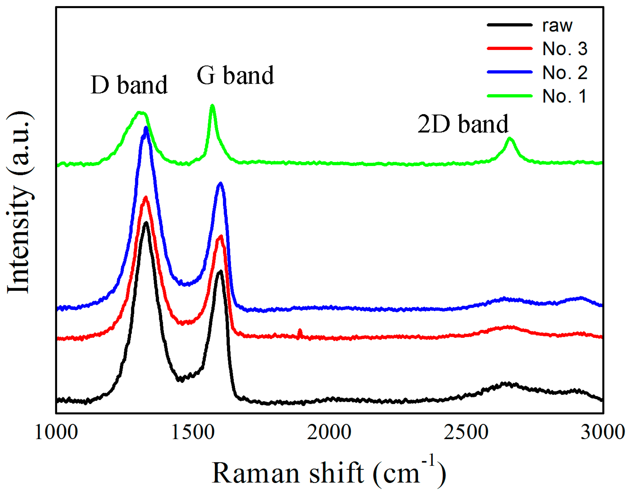
Figure 5 shows the Raman spectra of raw GO and the recovered samples, in which three characteristic bands of SP2 carbon were observed, including D band appearing at 1340 cm−1, G band at 1580–1600 cm−1, and 2D band at 2660 cm−1. The G band of the raw GO was detected at 1600 cm−1, showing an up-shift compared with that of graphite (around 1580 cm−1 [31]), which is in good agreement with the results reported in the literature [28,32,33]. When the charging voltage was 8–10 kV (samples No. 1 and 2), the G band was detected at 1595–1600 cm−1 (similar to that of raw GO), indicating the structure of original graphene films is well preserved. When the charging voltage was increased to 20 kV (No. 3), the G band was observed at around 1580 cm−1, similar to that of graphite, indicating the destruction of graphene structure and the formation graphite particles.
Figure 6 shows the X-ray photoelectron spectroscopy (XPS) spectra of raw GO and sample No. 1, in which the curve fitting was carried out by using Gaussian–Lorentzian peak shape after a Shirley background correlation. Based on Figure 7a,c, the C1s spectra of GO and sample No. 1 can be assigned to the non-oxygenated carbon (C=C/C–C) (284.7 eV) in the aromatic rings, and the carbon in C–O (286.2 eV) and O–C=O (288.2 eV) [34,35] in oxygen-containing functional groups. The Fe–C bond (283.3 eV) [36] is not observed in the C1s spectra; implying that Fe3C is not present in sample No. 1. Figure 7b,d show the O1s spectra of GO and sample No. 1; revealing the existence of C–O band (532.9 eV) and O–C=O band (530.9 eV) in GO and C–O band (532.9 eV), Fe–O–C (532.0 eV) and Fe–O band (529.9 eV) [29,37,38] in sample No. 1. The inset of Figure 6d shows the binding energy peaks of Fe0, Fe2+ (FeO) and Fe3+ (Fe2O3) [39,40] in sample No.1; demonstrating the existence of Fe and FeO nanoparticles and partial oxidation of Fe nanoparticles in this sample. The presence of the Fe–O–C bond demonstrates that the graphene films have been anchored with Fe or FeO nanoparticles by Fe–O–C bonds. Similar results are also reported by Zhou et al. in the research of magnetite–graphene nanosheet composites [29]. In addition to strong Fe–O–C bonding, the Fe and FeO nanoparticles may also link with the graphene films by other contact types, such as physisorption, electrostatic binding, covalent bond, and charge transfer interactions [29].
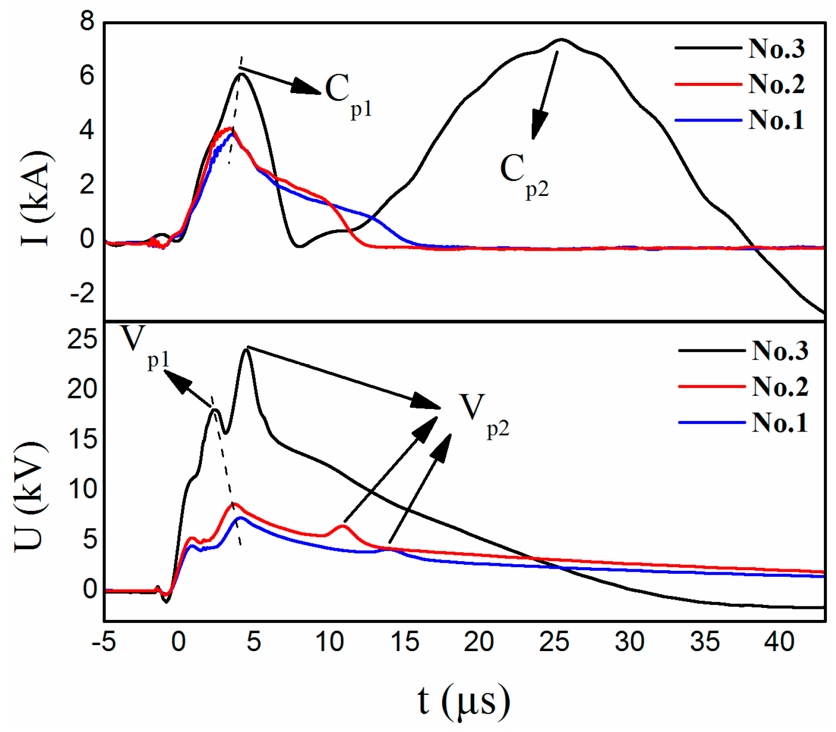
The discharge current and voltage during pulsed wire discharge have been controlled by the capacitance and charging voltage, as well as the phase transition of the wire, i.e., melting and vaporization [14,41]. The discharge current and voltage plots of samples No. 1–3 are shown in Figure 7. The first peaks of the discharge currents (CP1) were observed at approximately 3–5 μs in all three current plots, which are assigned to the joule heating process of pulsed wire discharge. During the ascending stage of CP1, the first peaks of the discharge voltages (Vp1) appeared in each test, indicating the increase of wire resistance as a result of melting during the joule heating process. During the rapid descending stage of Cp1, the second peaks of the discharge voltages (VP2) appeared in each test, implying a further increase of the resistance due to vaporization of the iron. Then, the hot iron dropped and the vapour spread out with a shock wave to form nanoparticles. In addition, Cp1, Vp1 and Vp2 were observed to come up earlier and become stronger with the increase of the charging voltage. However, it is noted that a second peak of the discharge current (Cp2) was observed for test No. 3, which is much wider and stronger than Cp1. This is caused by the strong arc discharge generated from the breakdown of the media between the two electrodes, when excessive stored energy is continuously injected following wire vaporization during the pulsed wire discharge process. The formation of strong arc discharge was also observed in other studies based on the analysis of discharge current and voltage [14,39] and the light emission signals due to arc discharge [42].
Based on the above analysis, we proposed the formation mechanism for Fe–FeO–Graphene nanocomposite during the pulsed wire discharge process. When an appropriate charging voltage is applied (8–10 kV for tests No. 1 and 2), a strong current passes through the iron wire, resulting in wire melting and vaporization due to the high temperature and pressure. The Fe vapour and droplets scatter out with a shockwave and cool down to form Fe and FeO nanoparticles. The formed Fe and FeO nanoparticles were anchored on the surface of graphene films due to the Fe–O–C bonding, which is formed because of the interaction between Fe and oxygen group on GO. When a higher charging voltage was applied (20 kV for test No. 3), a strong arc discharge was formed to generate high temperature plasma after the vaporization of the iron. The molecular structure of GO was destroyed by the plasma tunnel, resulting in the formation of graphite, amorphous carbon, Fe3C, and FeO(OH) due to chemical reactions.
4. Conclusions
In this work, Fe–FeO–graphene nanocomposites are obtained by exploding an iron wire in graphene oxide (GO) suspension. The composition and microstructure of the recovered products after pulsed wire discharge are largely influenced by the charging voltage. When proper charging voltages (8–10 kV) were applied, the molecular structure of graphene remained undestroyed and the iron wire melted and vaporized, producing Fe and FeO nanoparticles that were anchored on the graphene films. However, when the charging voltage was increased to 20 kV, a strong arc discharge was formed to generate high temperature plasma due to excessive energy injection. The molecular structure of GO can be destroyed, and chemical reactions between carbon and iron can be induced.
Acknowledgments
The authors would like to express their thanks for the financial support from the National Natural Science Foundation of China (Grant No. 11521062) and the State Key Laboratory of Explosion Science and Technology, Beijing Institute of Technology, China (ZDKT18-01).
Author Contributions
Xin Gao, Pengwan Chen and Kazuyuki Hokamoto conceived and designed the experiments; Xin Gao, Naoaki Yokota, Hayato Oda and Shigeru Tanaka performed the experiments; Xin Gao analyzed the data; Shigeru Tanaka and Kazuyuki Hokamoto contributed reagents/materials/analysis tools; Xin Gao wrote the paper.
Conflicts of Interest
The authors declare no conflict of interest. The founding sponsors had no role in the design of the study; in the collection, analyses, or interpretation of data; in the writing of the manuscript, and in the decision to publish the results.
References
- Novoselov, K.S.; Geim, A.K.; Morozov, S.V.; Jiang, D.; Zhang, Y.; Dubonos, S.V.; Grigorieva, I.V.; Firsov, A.A. Electric field effect in atomically thin carbon films. Science 2004, 306, 666–669. [Google Scholar] [CrossRef] [PubMed]
- Geim, A.K.; Novoselov, K.S. The rise of graphene. Nat. Mater. 2007, 6, 183–191. [Google Scholar] [CrossRef] [PubMed]
- Stankovich, S.; Dikin, D.A.; Dommett, G.H.B.; Kohlhaas, M.; Zimney, E.; Stach, E.A.; Piner, R.D.; Nguyen, S.T.; Ruoff, R.S. Graphene-based composite materials. Nature 2006, 442, 282–286. [Google Scholar] [CrossRef] [PubMed]
- Singha, V.; Jounga, D.; Zhaia, L.; Dasa, S.; Khondakera, S.I. Graphene based materials: Past, present and future. Prog. Mater. Sci. 2011, 56, 1178–1271. [Google Scholar] [CrossRef]
- Kuilla, T.; Bhadra, S.; Yao, D.; Kim, N.H.; Bose, S.; Lee, J.H. Recent advances in graphene based polymer composites. Prog. Polym. Sci. 2010, 35, 1350–1375. [Google Scholar] [CrossRef]
- Wang, X.X.; Yu, M.X.; Zhang, W.; Zhang, B.Q.; Dong, L.F. Synthesis and microwave absorption properties of graphene/nickel composite materials. Appl. Phys. A 2015, 118, 1053–1058. [Google Scholar] [CrossRef]
- Wu, Z.S.; Zhou, G.M.; Yin, L.C.; Ren, W.C.; Li, F.; Cheng, H.M. Graphene/metal oxide composite electrodes materials for energy storage. Nano Energy 2012, 1, 107–131. [Google Scholar] [CrossRef]
- Boparai, H.K.; Joseph, M.; O’Carroll, D.M. Cadmium (Cd(2+)) removal by nano zerovalent iron: Surface analysis, effects of solution chemistry and surface complexation modeling. Environ. Sci. Pollut. Res. 2013, 20, 6210–6221. [Google Scholar] [CrossRef] [PubMed]
- Jorfi, S.; Rezaee, A.; Moheb-Ai, G.A.; Jaafarzadeh, N.A. Pyrene removal from contaminated soils by modified fenton oxidation using iron nano particles. J. Environ. Health Sci. Eng. 2013, 11, 1–8. [Google Scholar] [CrossRef] [PubMed]
- Kanel, S.R.; Greneche, J.M.; Choi, H. Arsenic(V) removal from groundwater using nano scale zero-valent iron as a colloidal reactive barrier material. Environ. Sci. Technol. 2006, 40, 2045–2050. [Google Scholar] [CrossRef] [PubMed]
- Kim, D.K.; Zhang, Y.; Voit, W.; Rao, K.V.; Kehr, J.; Bjelke, B.; Muhammed, M. Superparamagnetic iron oxide nanoparticles for bio-medical applications. Scr. Mater. 2001, 44, 1713–1717. [Google Scholar] [CrossRef]
- Ma, X.X.; Tao, H.Q.; Yang, K.; Feng, L.Z.; Cheng, L.; Shi, X.Z.; Li, Y.G.; Guo, L.; Liu, Z. A functionalized graphene oxide-iron oxide nanocomposite for magnetically targeted drug delivery, photothermal therapy, and magnetic resonance imaging. Nano Res. 2012, 5, 199–212. [Google Scholar] [CrossRef]
- Jabeen, H.; Chandra, V.; Jung, S.; Lee, J.W.; Kim, K.S.; Kim, S.B. Enhanced Cr(VI) removal using iron nanoparticle decorated graphene. Nanoscle 2011, 3, 3583–3585. [Google Scholar] [CrossRef] [PubMed]
- Kotov, Y.A. Electric explosion of wires as a method for preparation of nanopowders. J. Nanopart. Res. 2003, 5, 539–550. [Google Scholar] [CrossRef]
- Zhou, Q.; Zhang, Q.G.; Yan, W.Y.; Liu, X.D.; Zhang, J.; Zhao, J.P.; Pang, L. Effect of medium on deposited energy in microsecond electrical explosion of wires. IEEE Trans. Plasma Sci. 2012, 40, 2198–2204. [Google Scholar] [CrossRef]
- Wada, N.; Akiyoshi, K.; Morita, K.; Hokamoto, K. Reaction synthesis of several titanium oxides through electrical wire explosion in air and in water. Ceram. Int. 2013, 39, 7927–7933. [Google Scholar] [CrossRef]
- Abdelkader, E.M.; Jelliss, P.A.; Buckner, S.W. Metal and metal carbide nanoparticle synthesis using electrical explosion of wires coupled with epoxide polymerization capping. Inorg. Chem. 2015, 54, 5897–5906. [Google Scholar] [CrossRef] [PubMed]
- He, L.F.; Shirahata, J.; Suematsu, H.; Nakayama, T.; Suzuki, T.; Jaing, W.; Niihara, K. Synthesis of BN nanosheet/nanotube-Fe nanocomposites by pulsed wire discharge and high-temperature annealing. Mater. Lett. 2014, 117, 120–123. [Google Scholar] [CrossRef]
- Kobayashi, R.; Nishimura, S.; Suzuki, T.; Nakayama, T.; Suematsu, H.; Jiang, W.H.; Niihara, K. Pressure dependence of phases in carbon nanosized powders for investigating cooling rate of pulsed wire discharge plasma. Adv. Mater. Res. 2006, 11, 307–310. [Google Scholar] [CrossRef]
- Suematsu, H.; Minami, C.; Kobayashi, R.; Kinemuchi, Y.; Hirata, T.; Hatakeyama, R.; Yang, S.C.; Jiang, W.H.; Yatsui, K. Preparation of fullerene by pulsed wire discharge. Jpn. J. Appl. Phys. 2003, 42, L1028–L1031. [Google Scholar] [CrossRef]
- Kobayashi, R.; Nishimura, S.; Suzuki, T.; Suematsu, H.; Jiang, W.H.; Yatsui, K. Synthesis of single-walled carbon nanotubes by pulsed wire discharge. Jpn. J. Appl. Phys. 2005, 44, 742–744. [Google Scholar] [CrossRef]
- Baklar, V.Y. Optimization of the synthesis of different carbon allotropes by electric explosion of graphite conductors. Surf. Eng. Appl. Electrochem. 2011, 47, 61–65. [Google Scholar] [CrossRef]
- Gao, X.; Xu, C.X.; Yin, H.; Wang, X.G.; Song, Q.Z.; Chen, P.W. Preparation of graphene by electrical explosion of graphite sticks. Nanoscale 2017, 9, 10639–10646. [Google Scholar] [CrossRef] [PubMed]
- Lee, H.J.; Shim, H.W.; Kim, J.C.; Kim, D.W. Mo-MoO3-graphene nanocomposites as anode materials forlithium-ion batteries: Scalable, facile preparation and characterization. Electrochim. Acta 2017, 251, 81–90. [Google Scholar] [CrossRef]
- Lee, D.H.; Kim, J.C.; Shim, H.W.; Kim, D.W. Highly Reversible Li storage in hybrid NiO/Ni/graphene nanocomposites prepared by an electrical wire explosion process. ACS Appl. Mater. Interfaces 2014, 6, 137–142. [Google Scholar] [CrossRef] [PubMed]
- Li, Y.H.; Du, Q.J.; Wang, J.J.; Liu, T.H.; Sun, J.K.; Wangy, Y.H.; Wang, Z.H.; Xia, Y.Z.; Xia, L.H. Defluoridation from aqueous solution by manganese oxide coated graphene oxide. J. Fluor. Chem. 2013, 148, 67–73. [Google Scholar] [CrossRef]
- Stobinski, L.; Lesiak, B.; Malolepszyc, A.; Mazurkiewiczc, M.; Mierzwaa, B.; Zemek, J.; Jiricek, P.; Bieloshapka, I. Graphene oxide and reduced graphene oxide studied by the XRD, TEM and electron spectroscopy methods. J. Electron Spectrosc. Relat. Phenom. 2014, 195, 145–154. [Google Scholar] [CrossRef]
- Marcano, D.C.; Kosynkin, D.V.; Berlin, J.M.; Sinitskii, A.; Sun, Z.Z.; Slesarev, A.; Alemany, L.B.; Lu, W.; Tour, J.M. Improved synthesis of graphene oxide. ACS Nano 2010, 4, 4806–4814. [Google Scholar] [CrossRef] [PubMed]
- Zhou, J.S.; Song, H.H.; Ma, L.L.; Chen, X.H. Magnetite/graphene nanosheet composites: Interfacial interaction and its impact on the durable high-rate performance in lithium-ion batteries. RSC Adv. 2011, 1, 782–791. [Google Scholar] [CrossRef]
- Xu, C.; Wang, X.; Zhu, J.W.; Yang, X.J.; Lu, L.D. Deposition of Co3O4 nanoparticles onto exfoliated graphite oxide sheets. J. Mater. Chem. 2008, 18, 5625–5629. [Google Scholar] [CrossRef]
- Reich, S.; Thomsen, C. Raman spectroscopy of graphite. Philos. Trans. R. Soc. A Math. Phys. Eng. Sci. 2004, 362, 2271–2288. [Google Scholar] [CrossRef] [PubMed]
- Mattevi, C.; Eda, G.; Agnoli, S.; Miller, S.; Mkhoyan, K.A.; Celik, O.; Mastrogiovanni, D.; Granozzi, G.; Garfunkel, E.; Chhowalla, M. Evolution of electrical, chemical, and structural properties of transparent and conducting chemically derived graphene thin films. Adv. Funct. Mater. 2009, 19, 2577–2583. [Google Scholar] [CrossRef]
- Tuinstra, F.; Koenig, J.L. Raman spectrum of graphite. J. Chem. Phys. 1970, 53, 1126–1130. [Google Scholar] [CrossRef]
- Moon, I.K.; Lee, J.; Ruoff, R.S.; Lee, H. Reduced graphene oxide by chemical graphitization. Nat. Commun. 2010, 1, 73–79. [Google Scholar] [CrossRef] [PubMed]
- Bagri, A.; Mattevi, C.; Acik, M.; Chabal, Y.J.; Chhovalla, M.; Shenoy, V.B. Structural evolution during the reduction of chemically derived graphene oxide. Nat. Chem. 2010, 2, 581–587. [Google Scholar] [CrossRef] [PubMed]
- Furlan, A.; Jansson, U.; Lu, J.; Hultman, L.; Magnuson, M. Structure and bonding in amorphous iron carbide thin films. J. Phys. Condens. Matter 2015, 27, 45002–45009. [Google Scholar] [CrossRef] [PubMed]
- Combellas, C.; Delamar, M.; Kanoufi, F.; Pinson, J.; Podvorica, F.I. Spontaneous grafting of iron surfaces by reduction of aryldiazonium salts in acidic or neutral aqueous solution. Application to the protection of iron against corrosion. Chem. Mater. 2005, 17, 3968–3975. [Google Scholar] [CrossRef]
- Chen, L.X.; He, F.; Zhao, N.Q.; Guo, R.S. Fabrication of 3D quasi-hierarchical Z-scheme RGO-Fe2O3-MoS2 nanoheterostructures for highly enhanced visible-light-driven photocatalytic degradation. Appl. Surf. Sci. 2017, 420, 669–680. [Google Scholar] [CrossRef]
- Bhargava, G.; Gouzman, I.; Chun, C.M.; Ramanarayanan, T.A.; Bernasek, S.L. Characterization of the ‘‘native’’ surface thin film on pure polycrystalline iron: A high resolution XPS and TEM study. Appl. Surf. Sci. 2007, 253, 4322–4329. [Google Scholar] [CrossRef]
- Leedahl, B.; Korolev, A.V.; Zhidkov, I.S.; Skornyakov, S.L.; Anisimov, V.I.; Belozerov, A.S.; Kukharenko, A.I.; Kurmaev, E.Z.; Grokhovskii, V.I.; Cholakh, S.O.; et al. Searching for pure iron in nature: The chelyabinsk meteorite. RSC Adv. 2016, 6, 85844–85851. [Google Scholar] [CrossRef]
- Taylor, M.J. Formation of plasma around wire fragments created by electrically exploded copper wire. J. Phys. D Appl. Phys. 2012, 24, 544–548. [Google Scholar] [CrossRef]
- Wong, C.S.; Bora, B.; Yap, S.L.; Lee, Y.S.; Bhuyan, H.; Farve, M. Effect of ambient gas species on the formation of Cu nanoparticles in wire explosion process. Curr. Appl. Phys. 2012, 12, 1345–1348. [Google Scholar] [CrossRef]
Figure 1.
An illustration of the pulsed iron wire discharge setup. 1—stainless steel chamber, 2—lid, 3—nsulation pipe, 4—electrodes, 5—insulation block, 6—plastic pipe, 7—graphene oxide (GO) suspension and 8—iron wire.
Figure 1.
An illustration of the pulsed iron wire discharge setup. 1—stainless steel chamber, 2—lid, 3—nsulation pipe, 4—electrodes, 5—insulation block, 6—plastic pipe, 7—graphene oxide (GO) suspension and 8—iron wire.
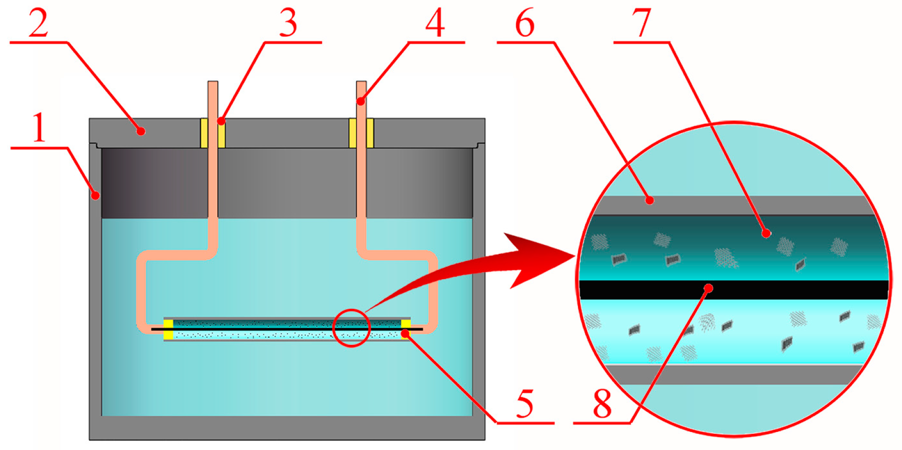
Figure 2.
X-ray diffraction (XRD) patterns of raw GO and samples No. 1–3. The insets of Figure 2 show the weak and broad peaks appearing at 9–30° in the XRD patterns of raw GO, samples No. 1 and 2.
Figure 2.
X-ray diffraction (XRD) patterns of raw GO and samples No. 1–3. The insets of Figure 2 show the weak and broad peaks appearing at 9–30° in the XRD patterns of raw GO, samples No. 1 and 2.

Figure 3.
Typical scanning electron microscopy (SEM) images of the recovered samples. (a) Typical SEM image, (b) higher-magnification view of sample No. 1, (c) Typical SEM image, and (d) higher-magnification view of sample No. 3.
Figure 3.
Typical scanning electron microscopy (SEM) images of the recovered samples. (a) Typical SEM image, (b) higher-magnification view of sample No. 1, (c) Typical SEM image, and (d) higher-magnification view of sample No. 3.

Figure 4.
Typical and high-resolution transmission electron microscopy (TEM) images of the recovered samples. TEM image (a) and high-resolution TEM image (b) of sample No. 1. TEM image (c) and high-resolution TEM image (d) of sample No. 3.
Figure 4.
Typical and high-resolution transmission electron microscopy (TEM) images of the recovered samples. TEM image (a) and high-resolution TEM image (b) of sample No. 1. TEM image (c) and high-resolution TEM image (d) of sample No. 3.
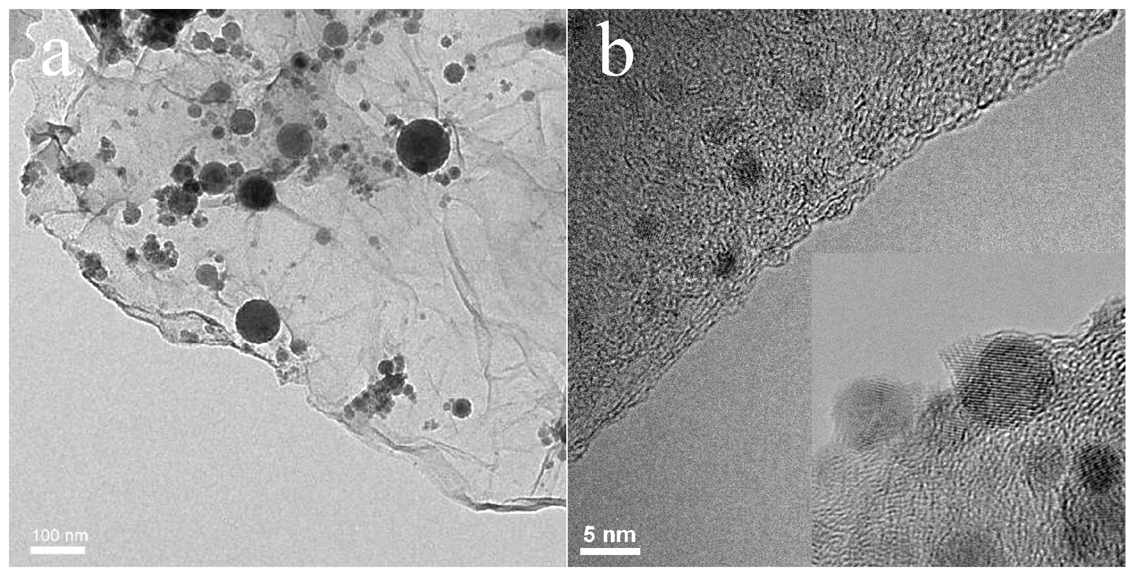

Figure 5.
Raman spectra of recovered samples produced by pulsed iron wire discharge in GO suspension. The spectrum of the raw GO is given for comparison.
Figure 5.
Raman spectra of recovered samples produced by pulsed iron wire discharge in GO suspension. The spectrum of the raw GO is given for comparison.

Figure 6.
X-ray photoelectron spectroscopy (XPS) spectra of GO and sample No. 1. (a) C1s spectrum, (b) O1s spectrum of GO, (c) C1s spectrum, and O1s spectrum (d) of sample No. 1. The inset of (d) shows the Fe2p spectrum of sample No. 1. The black line shows the original data, the red line shows the fitted curve of black line, and the other color dot lines are fitted curves for different specific bonds.
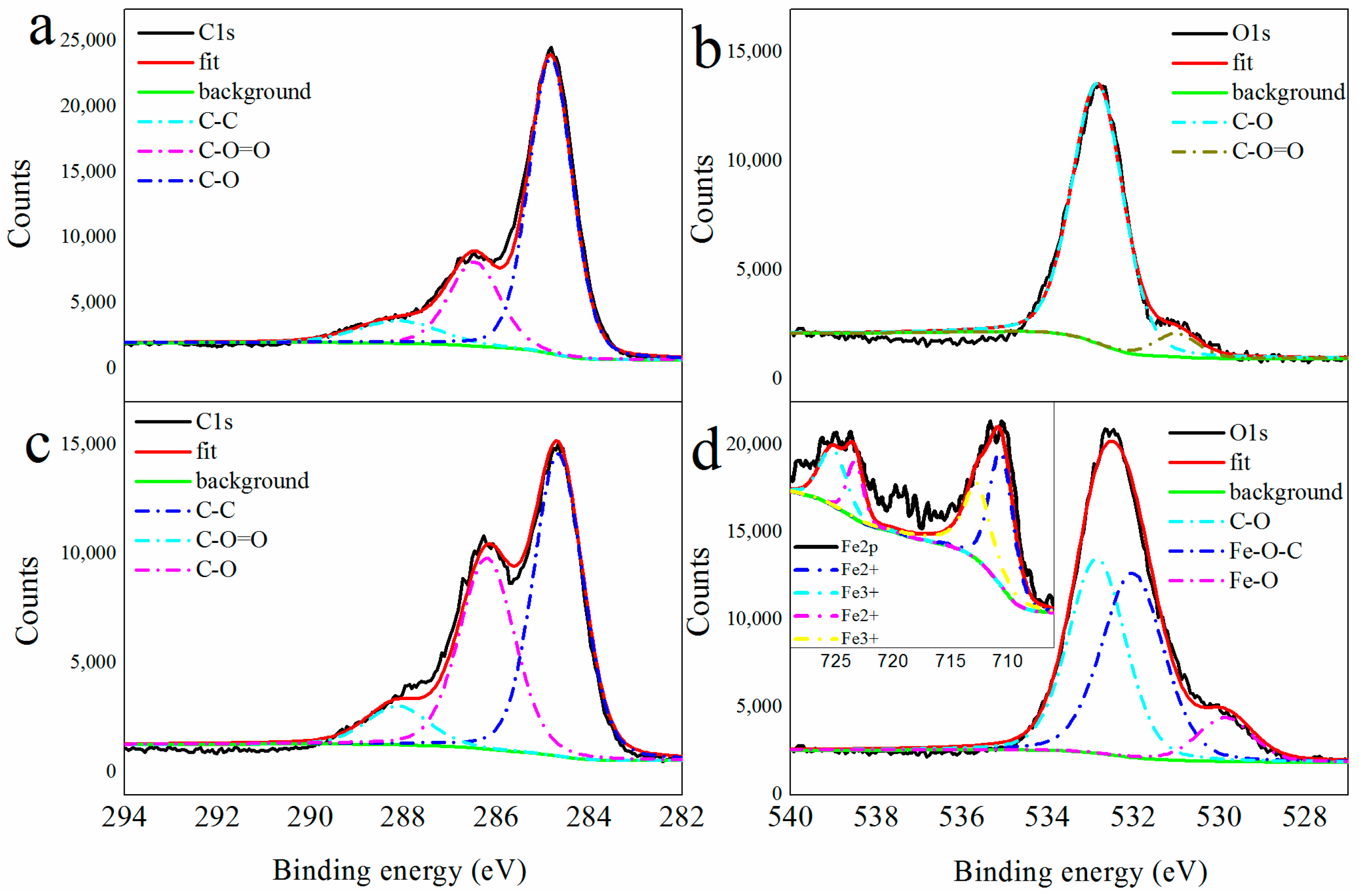
Figure 7.
Typical current and voltage plots of tests No. 1–3 tests. In the plots, the first and second peaks of discharge current are labelled as Cp1 and Cp2, respectively. The first and second peaks of discharge voltage are labelled as Vp1 and Vp2, respectively.
Figure 7.
Typical current and voltage plots of tests No. 1–3 tests. In the plots, the first and second peaks of discharge current are labelled as Cp1 and Cp2, respectively. The first and second peaks of discharge voltage are labelled as Vp1 and Vp2, respectively.


Table 1.
Experimental conditions of pulsed iron wire discharge and characterization of recovered samples 1.
Table 1.
Experimental conditions of pulsed iron wire discharge and characterization of recovered samples 1.
| No. | U (kV) | E (J) | Raman Spectra G Band (cm−1) | Main Products |
|---|---|---|---|---|
| 1 | 8 | 400 | 1600.5 | Fe, FeO, graphene |
| 2 | 10 | 625 | 1595.7 | Fe, FeO, graphene |
| 3 | 20 | 2500 | 1580.1 | FeO, Fe3C, FeO(OH), graphite particles |
1 U is the charging voltage and E is the energy stored in the capacitor.
Table 2.
Phase content of iron and iron compound of the recovered samples produced by pulsed iron wire discharge.
Table 2.
Phase content of iron and iron compound of the recovered samples produced by pulsed iron wire discharge.
| No. | Phase Content (%) | |||
|---|---|---|---|---|
| Fe | FeO | α-FeO (OH) | Fe3C | |
| 1 | 43 | 57 | 0 | 0 |
| 2 | 32 | 68 | 0 | 0 |
| 3 | 0 | 49 | 19 | 32 |
© 2018 by the authors. Licensee MDPI, Basel, Switzerland. This article is an open access article distributed under the terms and conditions of the Creative Commons Attribution (CC BY) license (http://creativecommons.org/licenses/by/4.0/).
Share and Cite
MDPI and ACS Style
Gao, X.; Yokota, N.; Oda, H.; Tanaka, S.; Hokamoto, K.; Chen, P. One Step Preparation of Fe–FeO–Graphene Nanocomposite through Pulsed Wire Discharge. Crystals 2018, 8, 104. https://doi.org/10.3390/cryst8020104
AMA Style
Gao X, Yokota N, Oda H, Tanaka S, Hokamoto K, Chen P. One Step Preparation of Fe–FeO–Graphene Nanocomposite through Pulsed Wire Discharge. Crystals. 2018; 8(2):104. https://doi.org/10.3390/cryst8020104
Chicago/Turabian StyleGao, Xin, Naoaki Yokota, Hayato Oda, Shigeru Tanaka, Kazuyuki Hokamoto, and Pengwan Chen. 2018. "One Step Preparation of Fe–FeO–Graphene Nanocomposite through Pulsed Wire Discharge" Crystals 8, no. 2: 104. https://doi.org/10.3390/cryst8020104
Note that from the first issue of 2016, this journal uses article numbers instead of page numbers. See further details here.