1. Introduction
Nanoscale structures have many applications, including integrated circuit manufacturing and biological applications. For example, biomimetic nanostructures with surface topography are used to study how living cells or micro-organisms respond to their environments [
1,
2,
3,
4,
5,
6]. In order to find the lower limit of biomimetic cellular response to surface topography, self-assembly regulated domain nanostructures of diblock copolymer have been exploited as a way to create templates for nanoscale patterning beyond the limit of conventional optical lithography [
7,
8,
9,
10,
11].
Diblock copolymer structures contain two chemically distinct polymer blocks. In liquid form, microphase separation between the two is observed, while in annealed solid thin films, the two blocks spontaneously self-assemble into nanoscale domains (~5 nm to 50 nm) that exhibit ordered morphology at equilibrium. The chemical distinction between the two polymer domains allows selective removal of one component of the structure by either wet etching or plasma etching. However, capillary forces associated with wet etching have been found to cause remaining structures to distort and collapse [
10,
12]. One of the most commonly used diblock copolymer is polystyrene-block-poly(methyl methacrylate) (PS-b-PMMA). We have previously developed a plasma etch process with high PMMA/PS etch selectivity and low surface roughness for selective removal of PMMA to produce high quality PS templates for patterning underlying materials.
In our previous study, a survey of etch gas mixtures [
12] showed that an Ar/O
2 plasma in combination with a high substrate bias voltage at −110 V (~125 eV ions) produced the best combination of etch selectivity and PS mask surface and line edge smoothness. Two particular results underlie this roughness study. First, PS and PMMA exhibit different surface roughness dependence on ion energy in O
2 and Ar/O
2plasma etching. Surface roughness of PS, as measured with atomic force microscopy (AFM) after plasma etching, decreases with increasing ion bombardment energy from ~25 eV to ~125 eV, while the opposite is observed for PMMA. Second, the surface roughness of PS after Ar/O
2 etching with high ion bombardment energy is lower than after O
2 plasma etching, suggesting that the higher ion to radical flux ratio expected with the Ar admixture plays a role in the reduced surface roughness.
The aim of this study is to identify mechanisms of surface roughening in plasma etching of polymers. Ar/O2 plasma etching of PS and PMMA is chosen as a case study, and the focus is on the role of cross-linking induced aggregation.
Surface cross-linking has been proposed as a factor in degradation during plasma etching of polymer materials [
13,
14,
15,
16]. During plasma exposure, ion bombardment causes breakage of the polymer backbone, side chain scissioning and depolymerization, collectively enhancing etch rate and mobility [
17,
18] in the surface layer. However, removal of H atoms and scissioning of chemical bonds in polymer chains also produces dangling bonds that may recombine to cross-link neighboring polymer chains. The resulting degree of cross-linking, associated with increased etch resistance, depends on the chemical structure of the polymer, the plasma gas mixture and ion bombardment energy. For example, one of the observed differences between PS and PMMA is the degree of cross-linking following plasma exposure. In the case of PS, surface cross-linking is prevalent, while in PMMA, chain scissioning and depolymerization dominate [
13,
14,
16]. While chemical structures such as the aromatic ring in PS and the methyl ester group in PMMA are commonly believed to play important roles in etching behaviors such as etch rate, cross-linking and chain scission, most studies reporting a correlation between chemical structures and etch behaviors of polymers are based on indirect observations, including change in molecular weight [
16], etch rate [
13,
19], interface adhesion [
14,
16] or diffusion coefficient [
20]. Details of the mechanisms involved have yet to be elucidated.
In addition, while O
2 plasmas are found to enhance cross-linking during PS etching through formation of C–O–C bonds, H and F atoms were shown to suppress cross-linking during plasma etching [
19]. H and F atoms form a single bond with C atoms, terminating dangling bonds and preventing cross-linking between C atoms in neighboring chains.
Cross-linking in plasma etching is also affected by ion bombardment energy. Tead
et al. [
20] studied the diffusion properties of O
2 plasma treated PS and suggested that cross-linking could cause reductions in mobility (ability of polymer to diffuse) and permeability at the surface layer of PS etched in O
2 plasmas. They demonstrated that higher ion energy could lead to greater cross-linking, resulting in reduced mobility and permeability.
Studies of the role of cross-linking in surface roughening of polymer etching are few. A correlation between cross-linking and aggregation leading to nano-scale inhomogeneity in mass and density has been proposed by Sumiya
et al. to explain surface roughening in polymer films [
21,
22,
23]. Polymer aggregation is commonly understood as the state when polymer chains are massed into dense tangled clusters. Studies of photoresist development in conventional optical lithography also suggest a correlation between cross-linking and aggregation in polymer materials. Yoshimura
et al. showed that cross-linking in photoresist materials could be exploited to create nanoscale microgel (aggregate like) structures [
24], similar to the model proposed by Sumiya
et al. [
21]. It has also been reported that molecular weight (MW) affects the size of intrinsic polymer aggregates [
26,
27].
A recent study of Ar etching of 193 nm photoresist by Chung
et al. [
17] showed that enhanced cross-linking could reduce surface roughening while higher levels of chain scissioning and mobility in the polymer could cause the opposite [
17,
18]. But rather than cross-linking induced aggregation as proposed in previous studies, a buckling theory [
17,
28] is proposed by Bruce
et al. to explain the mechanism behind this observation. In the proposed model, a stressed modified surface layer could buckle and form wrinkles and thus surface roughness during plasma etching. Cross-linking could increase the Young’s modulus of the modified surface layer and thus suppress buckling.
Different roughening mechanisms in plasma etching can be distinguished by characteristics such as form and size of roughness features during initial roughness formation and evolution. For example, during initial roughness formation, roughness features created by ion damage or deposition of sputtered materials are random in size and shape [
29,
30]. In contrast, roughness features induced by aggregation in polymer materials are more consistent in size and shape [
25,
31,
32,
33]. Roughness amplification mechanisms may also contribute to feature characteristics during roughness evolution. For example, in the “shadowing effect,” reactive radicals generated in the plasma have a lower flux in the “valleys” of surface topography than at the “peaks,” which block access to the valleys. Shadowing leads to either an increase or a decrease in the vertical dimension of existing roughness features depending on whether the radicals involved contribute to deposition or etching, respectively [
34,
35,
36]. In contrast, “flux re-emission” involves deflection or re-emission of energetic ions or radicals from feature sidewalls, increasing their relative flux at feature bottoms. Simulation results show smaller roughness features in valleys may disappear over time due to flux re-emission, leading to a decrease in concentration of features on the substrate surface as it evolves [
30,
34,
37,
38]. In “micro-masking”, small regions of greater etch resistance form on film surface, typically caused by redeposition of material sputtered from chamber walls. However, inhomogeneities induced in the modified film surface during plasma exposure may have a similar effect [
39].
The approach taken here to investigate the roles of cross-linking and aggregation includes examination of the role of aggregation in surface roughening by comparing initial roughness formation and evolution, using characteristics such as form and size of roughness features of Ar/O
2 etched PS and PMMA. In addition, the opposite dependence on ion bombardment energy of PS and PMMA surface roughness in Ar/O
2 plasma etching [
21] may offer insight into the role of cross-linking. A unique capability to independently select ion bombardment energy is utilized here in an examination of the role of cross-linking in surface roughening. Higher ion bombardment energy is known to enhance cross-linking in O
2 plasma etching of PS [
20], but has minimal effect on cross-linking in PMMA etching, in which chain scissioning dominates. Surface roughness of PS and PMMA films are characterized in this study with atomic force microscopy (AFM). Etch times are varied to observe initial roughness formation as well as further evolution resulting from plasma exposure, with the following variables: ion bombardment energy, monomer molecular weights and etch times. Studies of the effect of the energy of bombarding ions make use of a novel system in which the energy of bombarding ions is selected while maintaining a narrow energy spread compared to typical etch systems [
40].
Another set of experiments with Ar/H
2 and Ar/F
2 etching of PS and PMMA are designed to suppress the effects of cross-linking through the termination of dangling bonds by F or H atoms [
19]. Post-etch roughness of PS samples with different MWs are also compared to investigate the contribution of intrinsic aggregation in surface roughening. A model of surface roughening during plasma etching that involves cross-linking-induced aggregation is presented. In this model, differences between Ar/O
2 plasma treated PS and PMMA are attributed to modified layers with varying degrees of cross-linking on the surface of the etched polymer films.
Most reported studies of surface roughening compare surface roughness induced in plasma etching with different plasma conditions and with etch time or ion fluence held fixed [
41,
42,
43], resulting in considerable variation in corresponding etch depth due to etch rate differences. Etch rate [
41,
44] and roughening rate [
37,
44] might also change with time before a steady state is reached during etching. Here, samples are etched to the same etch depth (~150 nm) in most of the tests (except those examining roughness initiation) for studying the effect of gas mixtures and ion bombardment energy. This way, results are applicable to process optimization of etching processes with constant etch depth. In addition, the size of the roughness features on etched PS and PMMA samples is in a range up to ~20 nm. Etch depths greater than the size of the roughness are required to observe the mechanisms that contribute to the surface evolution after initial roughness is formed. As different gas mixtures, like O
2 and pure Ar, may produce differences in etch rate up to a factor of 100 [
12], a constant etch depth ensures comparison in the same etching/roughening regime.
2. Experiment Setup
All etching experiments were carried out in a helicon plasma tool [
40] equipped with a diode laser thin film interferometer for
in situ etch depth measurement [
45]. One advantage of the helicon plasma etch tool used in this study compared to more conventional reactive ion etch (RIE) tools is that the plasma source power and self-bias power are decoupled [
46], so that ion bombardment energy at the substrate can be varied independent of ion flux, by changing the self-bias voltage. A substrate bias system equipped with a combination of a programmable voltage wave form generator, a broad-band power amplifier, and a coupling capacitor is used to produce a specially tailored bias voltage wave form, described in more detail in Reference [
40]. The tailored wave form was introduced as a method to produce a narrow distribution of ion energies at the substrate, and has shown to be effective in improving etch selectivity of SiO
2 over Si [
47] and organosilicate glass (OSG) over Si
3N
4 and SiC [
48].
The ion bombardment energy (Ei) is determined by the difference between plasma potential Vp and the DC self bias voltage on the wafer (Vp-Vbias). The DC self-bias voltage (Vbias) is measured at the power cable between the blocking capacitor and the substrate holder. Vp in our process is estimated at ~15V while the self-bias voltage at the substrate without bias power output is −10V. Therefore the minimum ion bombardment energy is (Vp-Vbias) e = ~25 eV. The stage is described as “floating” when no bias power is applied. A floating rather than grounded electrode is chosen for the lowest ion energy level, as it is not possible to ground the surface of the insulating polymer films. The ion bombardment energy ranges from ~25 eV (Vbias = −10 V) to ~125 eV (Vbias = −110 V) in this study.
All samples were etched at a pressure of 10 mTorr. The substrate electrode temperature was controlled at 5 °C with 7 sccm of He flow to the backside of the wafer to ensure good thermal contact with the cooled electrode. For Ar/O
2, Ar/F
2 and Ar/H
2 gas mixtures, the flow rate ratios between Ar and O
2 and F
2 and H
2, respectively, is 10:1 with total flow of 55 sccm. The helicon source power was set at 300 W, producing a sufficiently low etch rate to enable good control of the etch depth [
12].
The PS homopolymer, with Mn of 60 kg/mole and PDI of 1.03, was purchased from Polymer Source. The PMMA solution is 4 wt% in anisole, bought from MicroChem Corp., with Mn of 950 kg/mole. PS test wafer are made by spin coating a 5 wt% PS solution in toluene at 2,000 RPM for 1 minute, followed by a 1 minute, 160 C bake, to produce a ~300 nm thick film. PMMA test wafers were made in the same way except the solution was used as purchased. Blanket PS and PMMA film samples of size 1 ° 1 cm2, cut from the 4”D wafers, are used for etch surface roughness measurements. All samples are mounted on a 4-inch bare silicon wafer with electrically and thermally conductive graphite adhesive before loading onto the wafer stage for plasma etching. The surface roughness of the etched samples was measured using AFM with a Veeco MultiMode Scanning Probe Microscope system in tapping mode. Etched silicon tips with force constant of 3.5 N/m have been used in the AFM measurement.
3. Results
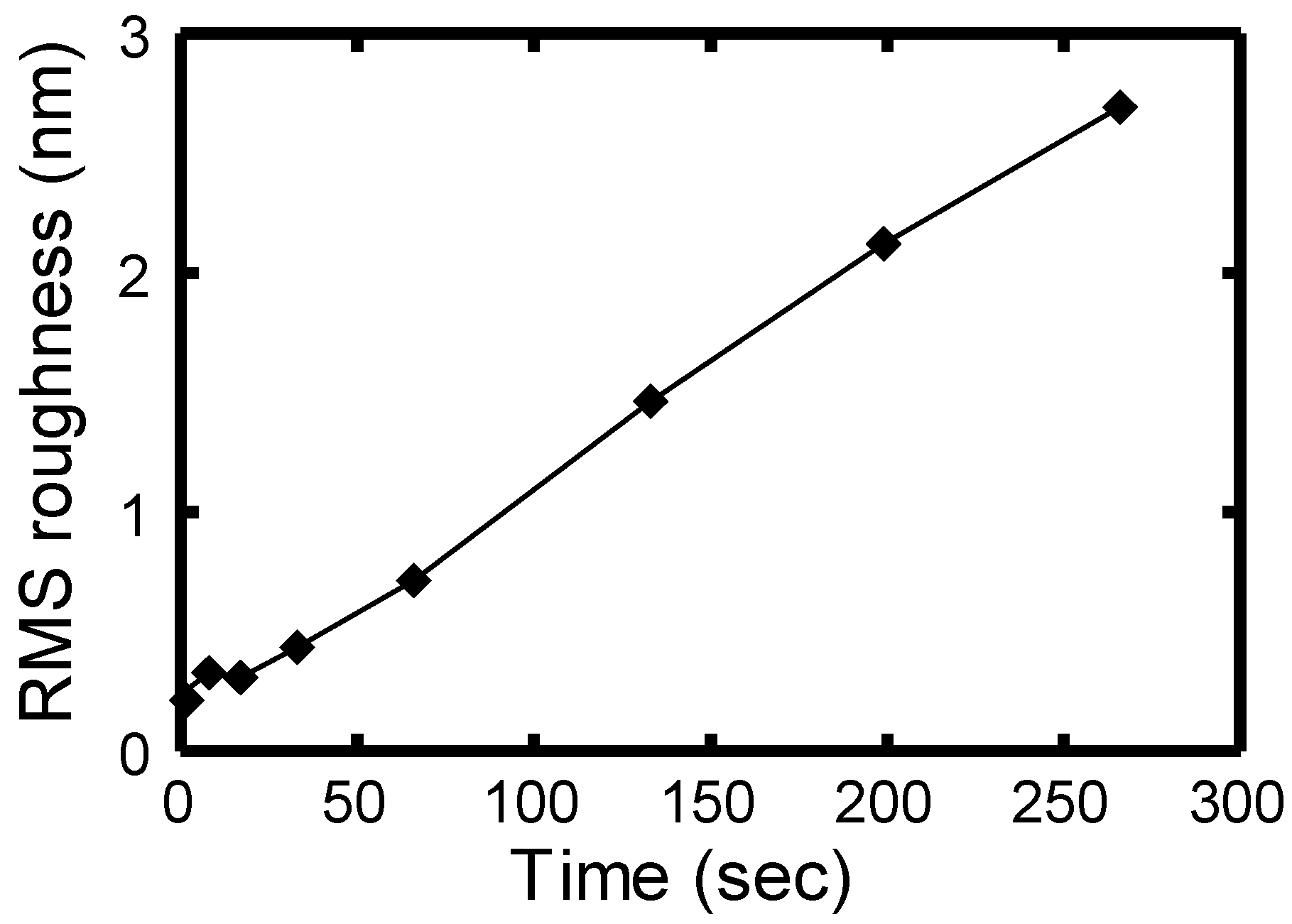
To characterize roughness initiation during plasma etching, PS blanket film samples etched with bias voltage of −10 V and etch time from 0 second to 266 seconds were measured with AFM.
Figure 1 and
Figure 2 show the AFM images and RMS roughness measurement results, respectively, for etched PS samples. Although surface roughness measurements show that RMS roughness increases almost linearly with time, roughness formation is divided into two stages base on AFM images. During the initial roughness formation (etch time from 0 seconds to 66 seconds), cone shaped roughness features appear and increase gradually in number on the surface [
Figure 1 (a–e)]. The roughness features show good uniformity in lateral size (~20 nm) and form, thus resembling the polymer aggregates observed in photoresist materials during development [
25,
31,
32,
33]. Initial roughness formation is very different from the initial roughness induced by common ion bombardment or redeposition of sputtered materials from the chamber wall that normally leads to craters or clusters of random size and shape. No metal impurities were detected by XPS measurements on plasma etched polymer samples, excluding the possibility of redeposition of chamber wall material. These results leave open the possibility that polymer aggregation may be involved in the initial roughness formation during PS etching.
Figure 1.
AFM images of Ar/O2 etched PS with bias voltage of −10 V and different etch times from (a) 0 seconds to (h) 266 seconds, corresponding to approximate etch depths (a) 0 nm, (b) 9 nm, (c) 18 nm, (d) 35 nm, (e) 70 nm, (f) 142 nm, (g) 212 nm and (h) 284 nm. Roughness features (white spots) of uniform size (~20 nm) and form initially increase in number over time during plasma etching, and subsequently increase in amplitude without further increase in number.
There are two possible causes of aggregation. It may be induced intrinsically throughout the film during polymer sample preparation [
31,
32,
33] or induced at the surface due to plasma exposure [
21]. If polymer aggregation is intrinsic, the inhomogeneity could induce etch rate non-uniformity immediately upon plasma exposure. Surface roughness features during initial roughness formation are expected to appear on the surface and saturate in number in short time after etching begins [
25]. But
Figure 1 shows that roughness features appear to start to saturate in number after etch times greater than 66 seconds, corresponding to etch depths of more than 70 nm, much larger than the size scale (~20 nm) of the roughness features. This result leads to the conclusion that roughness observed following Ar/O
2 plasma etching of PS does
not result from intrinsic inhomogeneity of the spun on film.
For etch times of 133 seconds and longer [
Figure 1 (f–h)], the number of roughness features on the surface has saturated. Increases in RMS (root mean square) roughness (
Figure 2) during this period are consistent with magnification of the surface roughness due to micro-masking. The consistency of the size and number of roughness features also supports the hypothesis that micro-masking plays a dominant role, and argues against flux re-emission [
39].
Figure 2.
RMS roughness of Ar/O2 etched PS with bias voltage of −10 V and etch times from (a) 0 seconds to (h) 266 seconds, corresponding to approximate etch depths (a) 0 nm, (b) 9 nm, (c) 18 nm, (d) 35 nm, (e) 70 nm, (f) 142 nm, (g) 212 nm and (h) 284 nm.
Figure 2.
RMS roughness of Ar/O2 etched PS with bias voltage of −10 V and etch times from (a) 0 seconds to (h) 266 seconds, corresponding to approximate etch depths (a) 0 nm, (b) 9 nm, (c) 18 nm, (d) 35 nm, (e) 70 nm, (f) 142 nm, (g) 212 nm and (h) 284 nm.
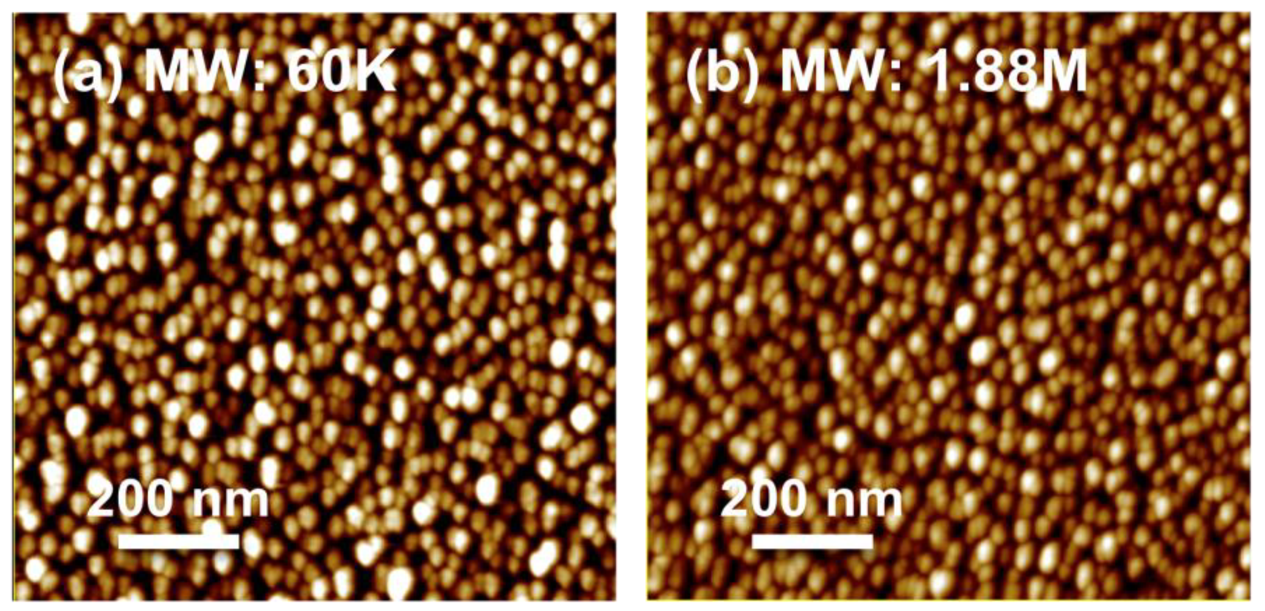
Etching experiments with polymers of different molecular weight (MW) were carried out as a further test for the contribution of intrinsic aggregation to roughness formation during etching. It has been reported that MW affects the size of intrinsic polymer aggregates [
26,
27]. Therefore, the sizes of surface roughness features on blanket PS films of different MWs etched with Ar/O
2 plasmas under identical conditions and etch duration are compared.
Figure 3 shows that etched PS samples of MWs of 60K g/mole and 1.88M g/mole exhibit surface roughness features of very similar height and lateral dimension, providing further evidence that the roughness observed is not due to intrinsic inhomogeneity.
The role of cross-linking is studied by observing the dependence of surface roughnesses of PS and PMMA on ion energy. Following both Ar/O
2 and O
2 plasma exposure, the surface roughnesses of PS and PMMA films show opposite dependence on ion energy [
12]. PS roughness decreases with increasing ion bombardment energy, while that of PMMA increases. A major difference between PS and PMMA is the level of cross-linking during plasma exposure, with the degree of cross-linking in PS is higher than in PMMA during plasma etching. Cross-linking in PS plasma etching may be further enhanced by increasing ion energy, leading to observed differences in surface roughness dependence on ion bombardment energy.
Figure 3.
AFM images of Ar/O2 etched PS with bias voltage of −10 V and molecular weights: (a) 60K g/mole (RMS: 4.92 nm), and (b) 1.88M g/mole (RMS: 4.19 nm) show similar surface morphology.
Figure 3.
AFM images of Ar/O2 etched PS with bias voltage of −10 V and molecular weights: (a) 60K g/mole (RMS: 4.92 nm), and (b) 1.88M g/mole (RMS: 4.19 nm) show similar surface morphology.
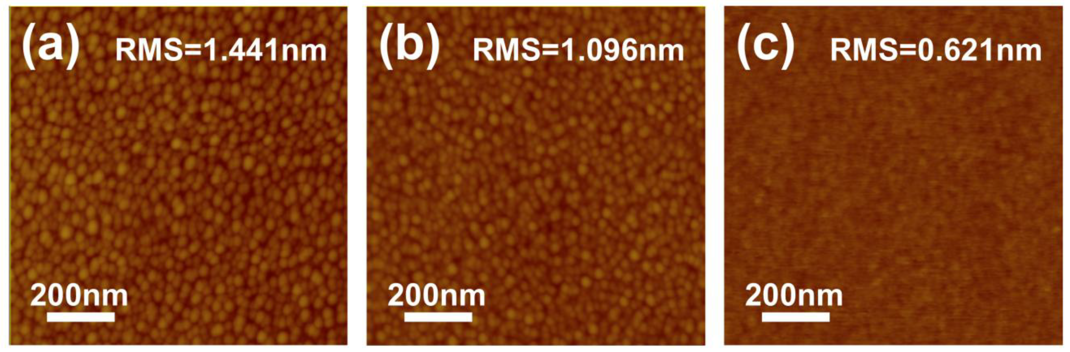
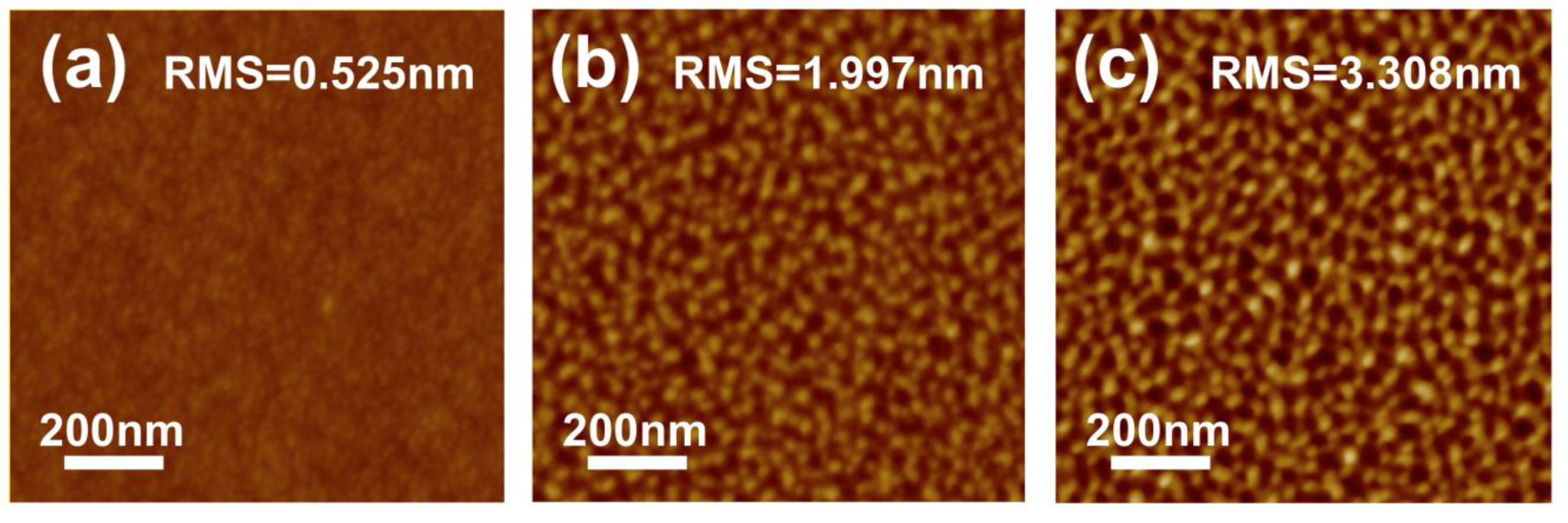
AFM images of Ar/O
2 etched PS and PMMA samples for three bias voltages: −10 V, −60 V and −110 V (ion energy: ~25 eV, −75 eV and 125 eV) are shown in
Figure 4 and
Figure 5, respectively. For PS, suppression of surface roughening is observed with increasing bias voltage. A proposed explanation is that for sufficiently high levels of cross-linking (higher bias voltages), a continuous etch resistant surface layer forms that suppresses roughness formation. In contrast, lower ion bombardment energies may produce a lower degree of cross-linking, such that cross-linking induced aggregation leads to heterogeneous etch resistance and thus greater surface roughness. For PMMA, surface roughening vanishes when the bias voltage is reduced to −10 V, perhaps because cross-linking, which has been shown to be lower in plasma etched PMMA than PS, is reduced to negligible levels under these conditions [
17,
18]. The formation of a continuous cross-linked etch resistant layer in PS during Ar/O
2 etching with high bombardment energy is consistent with etch rate measurements. When bias voltage is increased from −10 V to −110 V (ion energy from 25 eV to 125 ev), the PMMA etch rate increase by 345% while PS etch rate increase by only by 221% as shown in
Figure 6. This difference is mostly attributed to the enhanced cross-linking in PS at higher ion bombardment energy. While the dependence of surface roughness on ion energy is opposite for PS and PMMA etched in Ar/O
2, the surface roughness features are similar in size and form [
12] suggesting that the same roughening mechanism is involved.
Figure 4.
AFM images of Ar/O2 etched PS film with bias voltages of (a) −10 V, (b) −60 V and (c) −110 V.
Figure 4.
AFM images of Ar/O2 etched PS film with bias voltages of (a) −10 V, (b) −60 V and (c) −110 V.
Figure 5.
AFM images of Ar/O2 etched PMMA film with bias voltages of (a) −10 V, (b) −60 V and (c) −110 V.
Figure 5.
AFM images of Ar/O2 etched PMMA film with bias voltages of (a) −10 V, (b) −60 V and (c) −110 V.
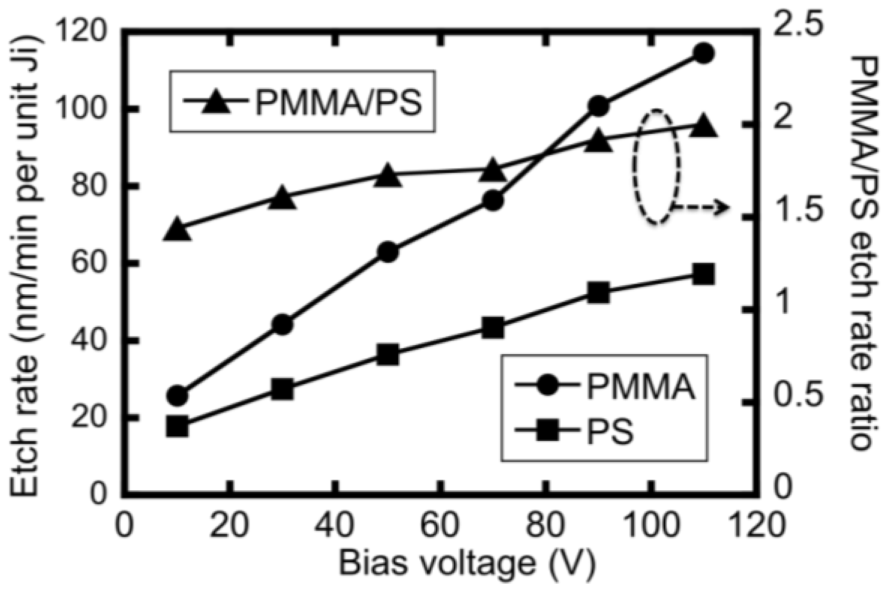
Figure 6.
PMMA etch rates in Ar/O2 show a higher increase (345%) than those for PS (221%), for bias voltage magnitudes of 10 V to 110 V.
Figure 6.
PMMA etch rates in Ar/O2 show a higher increase (345%) than those for PS (221%), for bias voltage magnitudes of 10 V to 110 V.
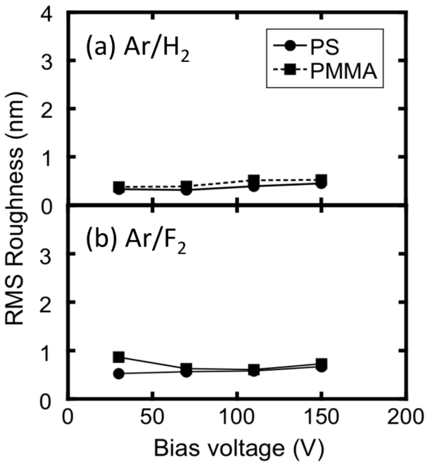
Figure 7.
RMS roughness of (a) Ar/H2 plasma and (b) Ar/F2 plasma etched PS films (circles) and PMMA films (squares) etched with different substrate bias voltages.
Figure 7.
RMS roughness of (a) Ar/H2 plasma and (b) Ar/F2 plasma etched PS films (circles) and PMMA films (squares) etched with different substrate bias voltages.
The role of cross-linking is further explored through the use of alternate etch gas mixtures that are expected to suppress cross-linking [
19]. Surface roughness of Ar/H
2 and Ar/F
2 etched PS and PMMA samples with four substrate bias voltages: −30 V to −150 V (ion energy: 45 eV to 165 eV) are shown in
Figure 7. Low RMS surface roughness levels of ~0.5 nm are observed in all samples tested, comparable to the unetched sample (~0.3 nm). Surface roughness features observed in Ar/O
2 etched PS and PMMA samples are not observed or significantly reduced. The suppression of surface roughness is thus attributed to the reduction in cross-linking associated with these etch gas mixtures.
4. Discussion
The data presented have been interpreted in the context of a model in which aggregation and cross-linking dominate surface roughening during polymer etching have been examined. The data may also be examined in the context of surface buckling, an alternative theory that predicts surface roughness with uniform size and shape [
17,
28], in which the highly-stressed carbon-rich modified surface layer buckles, producing wrinkles. The predicted surface roughness magnitude is affected by the wavelength of the wrinkles, the lateral dimension of the surface roughness features. Results of initial roughness formation and evolution are consistent with our speculation that aggregation is likely to be the origin of the surface roughening during plasma etching. The theory was previously supported by a correlation between the thickness of the modified layer and the lateral dimension of the roughness [
28].
Three observations reported herein are, however, not consistent with buckling theory predictions. First, initial roughness development in Ar/O
2 etching of PS shows that features are constant in size but increase in number during roughness formation (
Figure 1), while buckling theory predicts that roughness feature size should evolve during this transient period along the thickness of the modified layer. Second, ion bombardment energy during Ar/O
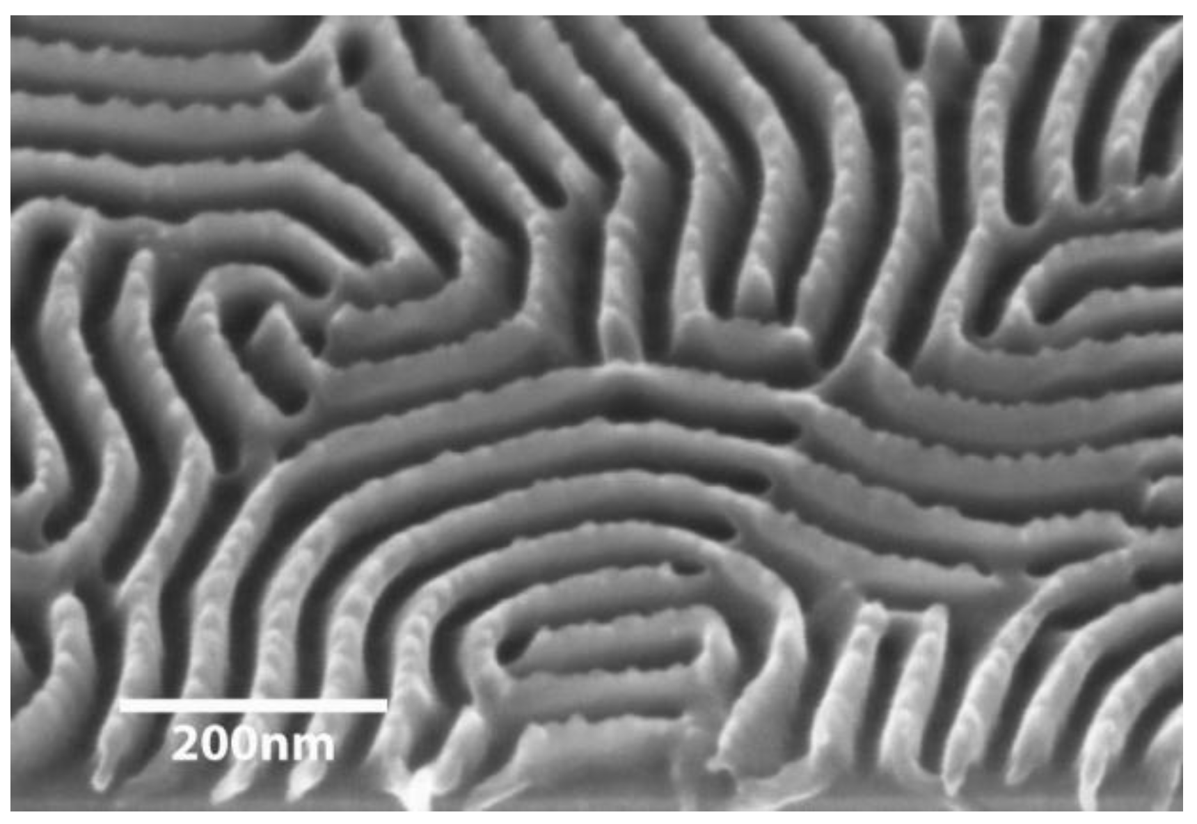
2 etching of PS and PMMA affects RMS roughness but not lateral feature dimensions, while buckling theory predicts that RMS roughness is correlated with lateral wrinkle dimension. Third, similar roughness features were observed on both blanket films and on the top surface of freestanding 25 nm lamellar PS structures following Ar/O
2 etching [
12], as shown in
Figure 8. A highly stressed surface layer on a freestanding structure is expected to exhibit different wrinkling behavior compared to a blanket film, as the added surface topography enhances stress release.
Figure 8.
Roughness features observed on the top surface of the freestanding lamellar PS structure after PMMA removal in block copolymer lithography have comparable dimensions to those on full film PS samples.
Figure 8.
Roughness features observed on the top surface of the freestanding lamellar PS structure after PMMA removal in block copolymer lithography have comparable dimensions to those on full film PS samples.
Conclusions from the data presented are summed up in a proposed cross-linking induced aggregation model to explain surface roughening in polymer etching. As mentioned in
Section I, during plasma etching, cross-linking and chain scissioning happen simultaneously at the film surface Breakage of polymer backbone bonds leads to a reduction in molecular weight and increased mobility [
17,
18], while cross-linking between adjacent polymer chains causes the opposite. In this picture, the balance between cross-linking and chain scission are a crucial factor in aggregation. If the rates of chain scissioning are comparable those of cross-linking, the mobility in this modified layer will be relatively high [
18]. The “stickiness” [
49] and recombination of dangling bonds in local cross-linking could trigger movement that leads to tangling or bundling of these polymer chains into aggregates on the surface [
21]. When, on the other hand, the rate of cross-linking dominates so that a continuous cross-linked layer forms, mobility as well as aggregation will be suppressed. If cross-linking between polymer chains is suppressed, for example, by passivation of dangling bonds with F or H atoms, aggregation may also be suppressed.
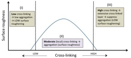
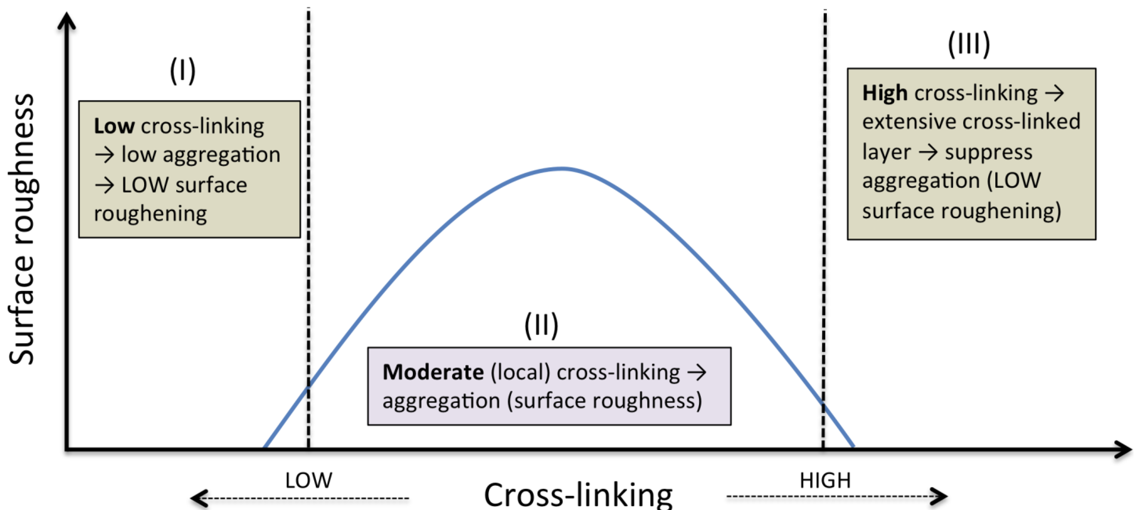
In this model, surface roughness following plasma etching is categorized in three regimes associated with the degree of cross-linking (
Figure 9). In Regime I, the rate of cross-linking is relatively low comparing to chain scissioning, so that aggregation and thus surface roughness are minimal. In Regime II, the rate of cross-linking is comparable to the rate of chain scissioning, inducing aggregation that leads to surface roughening. In Regime III, the rate of cross-linking is high, leading to an extensive cross-linked layer, suppressing mobility and aggregation, thus resulting in low surface roughness.
Figure 9.
Cross-linking induced aggregation model of formation of surface roughness during plasma etching of polymers.
Figure 9.
Cross-linking induced aggregation model of formation of surface roughness during plasma etching of polymers.
According to this model, surface roughness could be reduced by shifting the process away from Regime II to either Regime I or III. For example, in Ar/H2 and Ar/F2 etching of PS and PMMA, H and F atoms reduce the rate of cross-linking and suppress cross-linking induced aggregation, while a high rate of chain scissioning induced by ion bombardment is maintained (Regime I). Indeed, surface roughness vanishes in the samples etched in these gas mixtures.
In the case of Ar/O
2 plasma etching of PS, increasing ion bombardment energy enhances cross-linking in PS and shifts the process from Regime II toward Regime III. When the degree of cross-linking reaches a threshold where an extensive cross-linked layer is formed, aggregation is suppressed and etched films show lower surface roughness, as observed for ion bombardment energies of 125 eV and above in this study (
Figure 4).
For Ar/O2 etching of PMMA, in contrast, depolymerization is known to dominate over cross-linking under typical etching conditions. While cross-linking may be negligible at the lowest ion energies (Regime I), the balance between cross-linking and chain scissioning rates may shift sufficiently with increasing ion energy to produce low levels of aggregation and thus surface roughness (Regime II). Thus a possible explanation of the opposite roughening trends between PMMA and PS in Ar/O2 etching is that their respective etching regimes are different for a given ion energy.
Although a connection between surface roughness, cross-linking and aggregation is suggested by data presented here, improved methods are needed to quantify cross-linking and aggregation. Some groups have detected changes in cross-linking through the measurement of molecular weight (MW) by gel permeation chromatography (GPC) [
16]. However, attempts with this technique on the plasma etched polymers described herein failed because only the surface layer with thickness less than ~10 nm is modified by plasma etching. Therefore, the MW signal is dominated by the unmodified bulk of the polymer sample, masking any changes in MW in the surface layer. As more refined quantitative methods become available, a quantitative description of the relationships between surface roughness, cross-linking and aggregation will be possible.


