Article

Digital Integration of LiDAR System Implemented in a Low-Cost FPGA

1
School of Electronics and Communication Engineering, Guangzhou University, Guangzhou 510006, China
2
School of Mechanical and Electrical Engineering, Guangzhou University, Guangzhou 510006, China
*
Authors to whom correspondence should be addressed.
Symmetry 2022, 14(6), 1256; https://doi.org/10.3390/sym14061256
Submission received: 23 May 2022 / Revised: 9 June 2022 / Accepted: 13 June 2022 / Published: 17 June 2022
(This article belongs to the Special Issue New Advances in New-Generation Communication and Symmetry)

Abstract

:
With the development of artificial intelligence, LiDAR finds significant applications in robotics and autonomous driving. Aiming at increasing the compactness and the integration of 2-D LiDAR, this paper presents a highly digitally integrated 2-D LiDAR system implemented in a low-cost FPGA. The system is made of off-the-shelf components to limit the cost to USD 100. A laser transceiver with a symmetrical transmitting and receiving lens emits and collects laser pulses to range distance using the time-of-flight (ToF) method. As a key component in ToF, the FPGA-based time-to-digital converter (TDC) is adopted for counting the round-trip time of pulses, which is implemented in a low-cost FPGA of ZYNQ7010 with limited resources. The symmetrical structure of the delay line is used to design a more efficient TDC. The FPGA-TDC enables flexibility of design and integration with more functional logics and is microcontroller-free. All the digital logics including data processing and controlling are integrated into an FPGA with the TDC logics to realize fully digital integration and compact dimensions. The utilization of the whole architecture in the FPGA is about 15%. The experimental results demonstrated that the ranging accuracy of the LiDAR is about 2 cm, which is suitable for consumer electronics.
Keywords:
TDC; FPGA; LiDAR

1. Introduction

LiDAR is an acronym for light detection and ranging, which is the optical analog of radar. As an active sensor acquiring surrounding 3D information, LiDAR occupies key positions in remote sensing, defense, and autonomous driving [1,2,3,4,5]. A LiDAR generally consists of three key modules: transmitting, beam steering, and receiving modules. It obtains the distance of targets by illuminating laser signals at specific wavelengths on targets, and it obtains further 3D information by scanning the surface of the target in a mechanical or electromagnetic manner. Depending on different ranging principles, laser beams are modulated in time, frequency, or amplitude [6,7,8,9]. The ToF ranging principle that modulates laser beams in the time domain is a widely used distance measurement manner for LiDAR. The emitter illuminates a laser pulse to a target, and the receiver collects the reflected laser pulse. The ToF method measures distance by counting the round-trip flight time of emitted laser pulses between the LiDAR and the target. Timing is the key to distance measurement for a ToF LiDAR; its accuracy is crucial to the ranging accuracy of the LiDAR [10]. To reach accurate timing, a TDC is adopted to measure the time interval between the emission and the arrival of laser pulses. TDC is a chip that counts time between the start and stop signals and converts time intervals to measurable digital format. It can be considered as a combination of a time–analog and analog-to-digital converter to measure time intervals down to the picosecond range and convert time intervals from analog signal to digital signal [11,12]. Due to the high time resolution, TDC chips have been widely used in various areas, including high-energy physics [7], fluorescence lifetime spectroscopy in biology [13], and ToF ranging [14]. Realization of a TDC based on ASIC and realization of a TDC based on FPGA are the two main implementation techniques at present. The ASIC-TDC holds advantages of low price (mass production) and compact size. However, the limited reconfiguration, huge R&D cost, and a long development cycle make the ASIC-TDC unsuitable for projects with specific parameters, low cost, and fast development requirements. A commercial ASIC-TDC requires a micro-controller for the configuration of time counting, which is unfriendly to low-cost LiDARs. Compared to an ASIC-TDC, the implementation of a TDC in an FPGA cuts down the R&D cost and development cycle. Owing to the high reconfigurability of FPGAs, the FPGA-TDC also has the advantages of reconfigurable TDC architectures and integration with more functional logics. Numerous TDC architectures such as phased locks, delay lines, the Vernier method, and pulse shrinking have been implemented in FPGAs [15,16,17,18,19,20,21,22,23,24]. The harmonic ring oscillator structure achieved 347 ps bin size TDC in a Virtex-6 FPGA [15]. A 16-channel FPGA-TDC with 120 ps per LSB was implemented in a Virtex-4 FPGA for particle detectors [18]. For higher resolution, a TDC system with 16 ps RMS was achieved by subdividing the delay cell [19]. A fully fledged FPGA-TDC with self-test and temperature compensation was proposed to achieve a resolution of 50 ps [23]. However, architectures with high precision require high-end FPGAs and complicated logical methods with a large amount of resource utilization in FPGAs limits their applications in cost-sensitive areas such as consumer electronics, wearable devices, and IoT. A TDC circuit is used for pulse LiDAR [25]. However, the precise temporal resolution is only 290 ps. In [26], the author used a complex structure to integrate TDCs in a CMOS LiDAR for scanning, but the resolution is only 156.25 ps. In [27], the author used a Leddar M16 LiDAR sensor for real-time pedestrian counting. The cost is more than USD 1100, and the precision is about 6 cm. In [28], the author used a Teensy microcontroller, a commercial single-point LiDAR module, and many ASIC chips. The cost of the LiDAR system mentioned above is more than USD 150. Therefore, this paper proposes a TDC based on an FPGA with a simplified structure and low resource occupation, which is more suitable for a 2-D LiDAR system. To our best knowledge, there is almost no LiDAR system built using a single FPGA chip with TDC inside. Due to the motivation of this paper toward low-cost LiDAR, the cost of the demonstrated LiDAR system is less than $100 with approximate precision of 2 cm, lower than most reported LiDARs.
In this paper, we aim to demonstrate a fully FPGA-controlled and -processed low-cost digitally integrated LiDAR together with TDC implemented in a low-end FPGA chip with limited configurable logic block resource. For a LiDAR system, multiple MCU and ASIC chips are required to realize the control and processing functions of a 2-D LiDAR, including pulse control, motor control, ToF calculation, and data processing. With the capability of parallel and concurrent processing, an FPGA can realize high-speed computation in the form of a relatively low-cost coprocessor. This paper integrates all logic functions of a 2-D LiDAR in a single low-end FPGA. Through the digital synthesis technique, the FPGA generates the narrow pulse to trigger the laser. The FPGA-TDC realizes the ToF calculation and eliminates wiring delay. To reduce the complexity of the timing architecture and the resource utilization in FPGA-based LiDAR, a lightweight architecture of the tapped delay line was adopted to realize the TDC for ToF measurement. To achieve resource-saving utilization and consistent time in each delay unit, the entire CARRY4 cell is used as a delay unit to construct the delay line in our work. The timing accuracy of the proposed FPGA-TDC is about 80 ps, corresponding to a ranging accuracy of not more than 3 cm, which is applicable for most applications in consumer electronics [29,30]. Owing to the reduced resource utilization and high reconfiguration, the LiDAR control and data processing logics can be both implemented in the same FPGA chip using the rest of the resources. Except for the analog transceiver, all the digital logics operate in one FPGA chip to improve the integration and compactness of the LiDAR. Moreover, the high integration reduces the complexity of distance correction. The rest of the paper is organized as follows: (1) the principle of the FPGA-TDC is presented in Section 2; (2) the implementation methodology of the TDC and the performance of the tapped delay line are elaborated in Section 3; (3) the circuit design of laser transceiver module and the assembled prototype of LiDAR are demonstrated in Section 4; (4) the test results are discussed in Section 4; (5) a summary of our work is presented in Section 5.

2. Principle of the FPGA-TDC

The principle of the ToF ranging is to measure the traveling time of particles or waves between the emitter and the target. Counting clock pulses is the simplest method to measure the time interval between two events. The basic principle of the pulse counting method is the calculation of the number of system clock signals generated by the IHIT signal (time interval between two events) in its valid time. It can be easily implemented by starting and stopping a counter in an FPGA. However, for general asynchronous IHIT signals, the system clock cannot accurately measure the specific time interval due to the low resolution of the system clock in the FPGA. The limited time resolution of the pulse counting method by the clock period of the FPGA impeded the applications of the FPGA-TDC. Hence, a smaller timing unit is needed to improve the resolution of the time interval measurement. The widely used architecture without complicated operations to achieve a higher resolution is the tapped delay line [31]. The principle of the delay line is depicted in Figure 1; the delay line consists of multiple delay cells and a D-type flip-flop (FFD) array. These delay cells are organized in series forming a tapped delay line. The start signal is injected from the head of the delay line and propagates along the whole line in a single direction. Each time the signal passes through a delay cell, the state of the delay tap changes in binary. The FFDs are used to latch the state of delay taps. The clock ‘enable’ signal is activated when a signal enters the delay line for propagation. At the arrival of the positive clock edge, the positions of the delay cells are recorded in the form of the thermometer code.
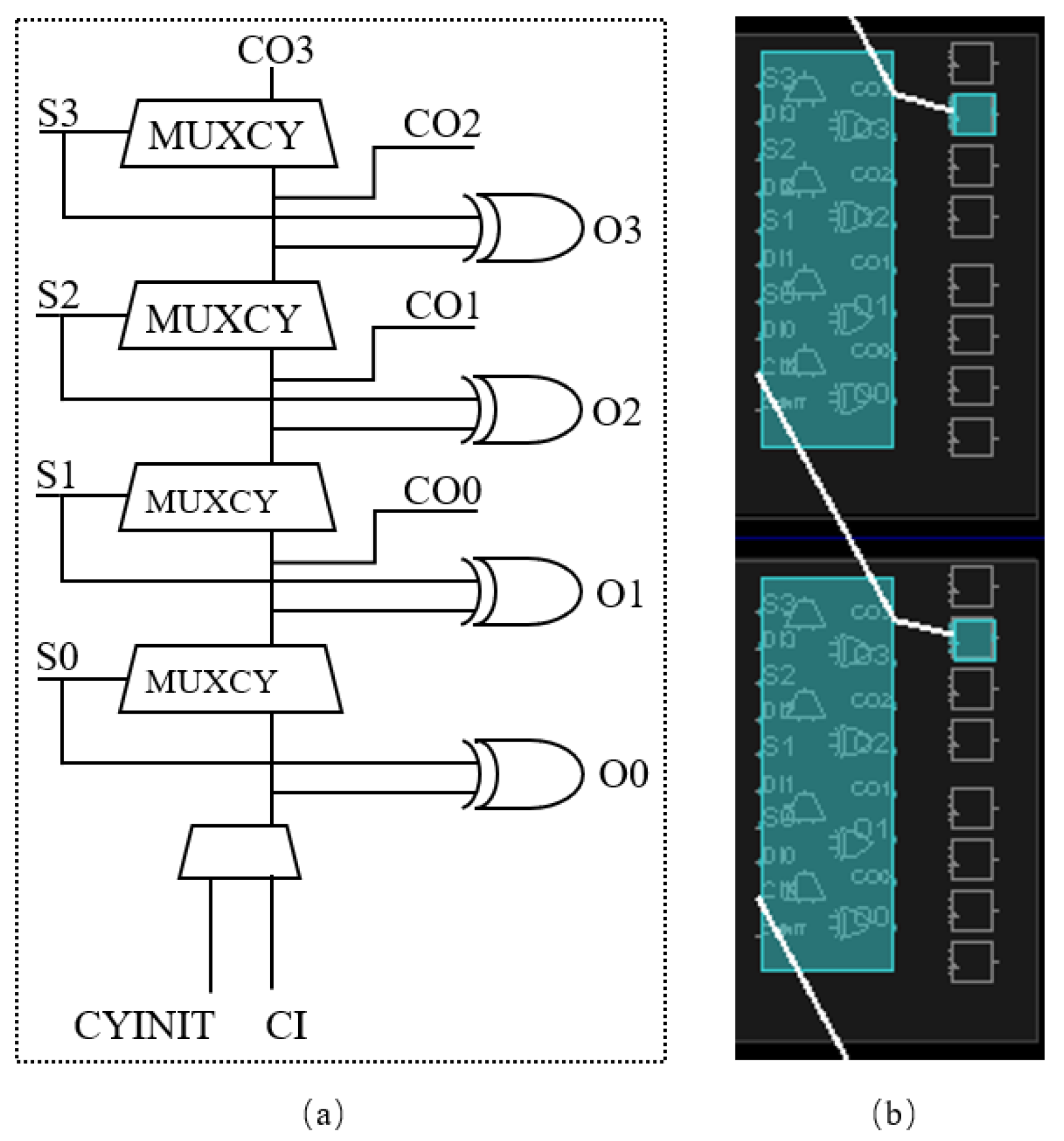
Located in the slice of the configurable logic block, the fast carry logic with the look-ahead element is CARRY4, which can be utilized as the time interpolator to build the tapped delay line. The simplified schematic of CARRY4 in FPGA is depicted in Figure 2a. Each CARRY4 cell consists of four multiplexers (MUXCY) and four XOR gates. Port CI is the input of the start signal, and CO3 is the output port of the delay line. In order to form a long delay line, several CARRY4 cells need to be cascaded into an array. The implementation of CARRY4 cells in the delay line logic is presented in Figure 2b. Firstly, the start signal is injected from the CI port of the first delay cell. Then the signal propagates through the MUXCY and is output from the CO3 port. The CO3 port is used for cascading into the CI port of the next delay cell. With the above cascade, the carry delay chain can be constructed. Subsequently, the state of the CO3 port latched by the FFD close to the line is the raw fine time data used for further operation. According to the route of the signal propagating in CARRY4, the time resolution of the FPGA-TDC is determined by the time interval of the signal crossing a delay cell, which is equivalent to the time required for signal propagation from CI to CO3. It must be noted that the CARRY4 can be subdivided into smaller delay cells for higher resolution. For the sake of the resource-saving implementation and the consistent time in each delay unit, the entire CARRY4 element is used as a delay unit in our architecture. The symmetric delay line structure is adopted to constitute the delay line with the same delay time.
An FPGA-TDC generally consists of two essential measurement blocks: the coarse counter and the fine counter [32]. The time interval longer than the full clock period is counted directly by the coarse one, while the time interval shorter than a full system clock period is measured by the fine one. In ToF ranging, the laser trigger signal depends on the system clock of the controller, so the coarse counter is synchronized with the pulse transmitter operating at the same time. For simplification, the trigger signal is synchronized with both the system clock and the start signal of the TDC. The time of electron–photon conversion and photon accumulation to form a laser pulse can be considered to be constant and corrected by further data processing.
The time measurement process is illustrated in Figure 3. In the beginning, the start signal is at a high logical level and the coarse counter starts to work simultaneously. When the stop signal is activated, the fine counter is triggered to work. The time values of both the coarse and fine counters are latched and recorded at the next rising edge of the system clock. Consequently, the time interval of an event can be expressed as follows:
T t o t a l = T c o a r s e T f i n e
where T c o a r s e denotes the number of clock periods between the start and stop and   T f i n e denotes the time interval between the rising edge of the stop and the rising edge of the next system clock.

3. TDC Implementation

3.1. Input Filter

The asynchronous input signal needs to be processed by the signal filter before being injected into the delay line. In the case of the input signal being longer than the system clock, it is necessary to shorten the input signal and keep the delay line active within one system clock. In this way, the delay line could obtain one available conversion value per input signal among possible multiple input signals. The schematic of the input filter and the simulation result are shown in Figure 4. The input filter consists of two discrete FFDs and an inverter. The signal represents the input event acting as a clock signal for the first FFD. The output of the first FFD is the reset bit for the two FFDs. Through an inverter, the filtered signal can be obtained from the output port of the second FFD. In the simulation, the input filter was tested by injecting a pulse signal, and the waveform of the signals was observed by a logic analyzer. The logic analyzer result shows that the input pulse is shortened by this means, which can be used to feed the delay line.

3.2. Implementation of the FPGA-TDC

The proposed FPGA-TDC was realized in a ZYNQ-7010 (XC7Z010) SoC. The implementation block diagram of the proposed TDC is depicted in Figure 5a. The architecture consists of a coarse counter, a tapped delay line, a series of FFDs, and a thermometer-to-binary decoder. The IHIT signal is obtained from an FFD based on the start and stop signal, representing the time interval to be measured. In addition, it is used as the standard signal for the coarse counter to be measured. The coarse time is measured by counting the number of 100 MHz clock periods of the IHIT signal, meaning that the coarse bin is 10 ns. In fine measurement, the filtered stop signal is fed to the tapped delay line. Once the hit signal occurs in the delay line, each bit of the delay line will change to logic ‘1′ step by step. The fine raw data of the delay line could be captured by the adjacent FFD array and sent to the thermometer-to-binary decoder. The decoder module detects the bit change of the fine data between ‘0′ and ‘1′ and converts the data from the form of thermometer code into binary code to obtain the fine conversion, making it readable for the subsequent step.
In order to get one least significant bit (LSB) delay time for the fine counter, the average delay LSB is adopted as the delay time per cell. The average LSB value is obtained by using the average calibration method. The delay line is constructed with more than two sampling clock cycles, and the number of delay cells is recorded when the delay line taps are sampled twice. Assuming that the number of samples for the first time is N 1 , the number of samples for the second time is N 2 , and the sampling clock period is T, the average delay LSB is as follows:
  LSB = T N 2 N 1
As shown in the inset in Figure 5a, the fine values sampled twice by the 100 MHz clock are about 8′h6E (8′d110) and 8′hE9 (8′d233). According to the above equation, the carry progression of the fine counter is about 123 bits under the sampling of the 100 MHz clock. Thus, the average LSB of the fine counter in TDC is about 81.3 ps. The tapped delay line of the fine TDC comprises 123 delay cells to cover a system clock period. The simulation results of the FPGA-TDC, including the start, stop, and IHIT signals; coarse time; and fine time are shown in Figure 5b. It is obvious that the IHIT signal is determined by the rising edges of start and stop signals. At the arrival of the stop signal, the coarse counter obtains the measurement value. The fine value is obtained at the arrival of the next rising edge of the system clock. The precise time interval is then obtained by combining the coarse counter and fine counter.

3.3. Evaluation

The LSB of the TDC is affected by the semiconductor fabrication process and external environments. The function of the differential nonlinearity (DNL) is adopted to analyze the LSB difference between the actually converted and the ideal values, and the integral nonlinearity (INL) is the accumulation sum of the DNL [33]. The typical code density test method and the bin-by-bin calibration [34] are used to calculate DNL and INL. The principle of the method is to generate a large number of external random pulses as the TDC input and record the times of each delay cell. The measurement of the statistical code is used to evaluate the overall resolution. The counting result of each time is stored in the system random access memory (RAM). The RAM configuration process is depicted in Figure 6. For obtaining the code density, the external pulses with no correlation to the TDC system clock are generated to be the trigger signal of the TDC, and the 100 MHz clock is used as the sampling clock. The Obin_data is the binary code from the fine conversion and used for addressing in the RAM. The hit pulse falls in a random delay cell, the times with the corresponding address in RAM increase by one, while the address and frequency are retained during periods without hit pulses. In order to prevent the address from adding multiple times in a single acquisition, it is necessary to configure the enabling port of the RAM. The rising edge of the external pulse signal is configured as the enabling signal to keep the register data in RAM consistent with the hit pulses.
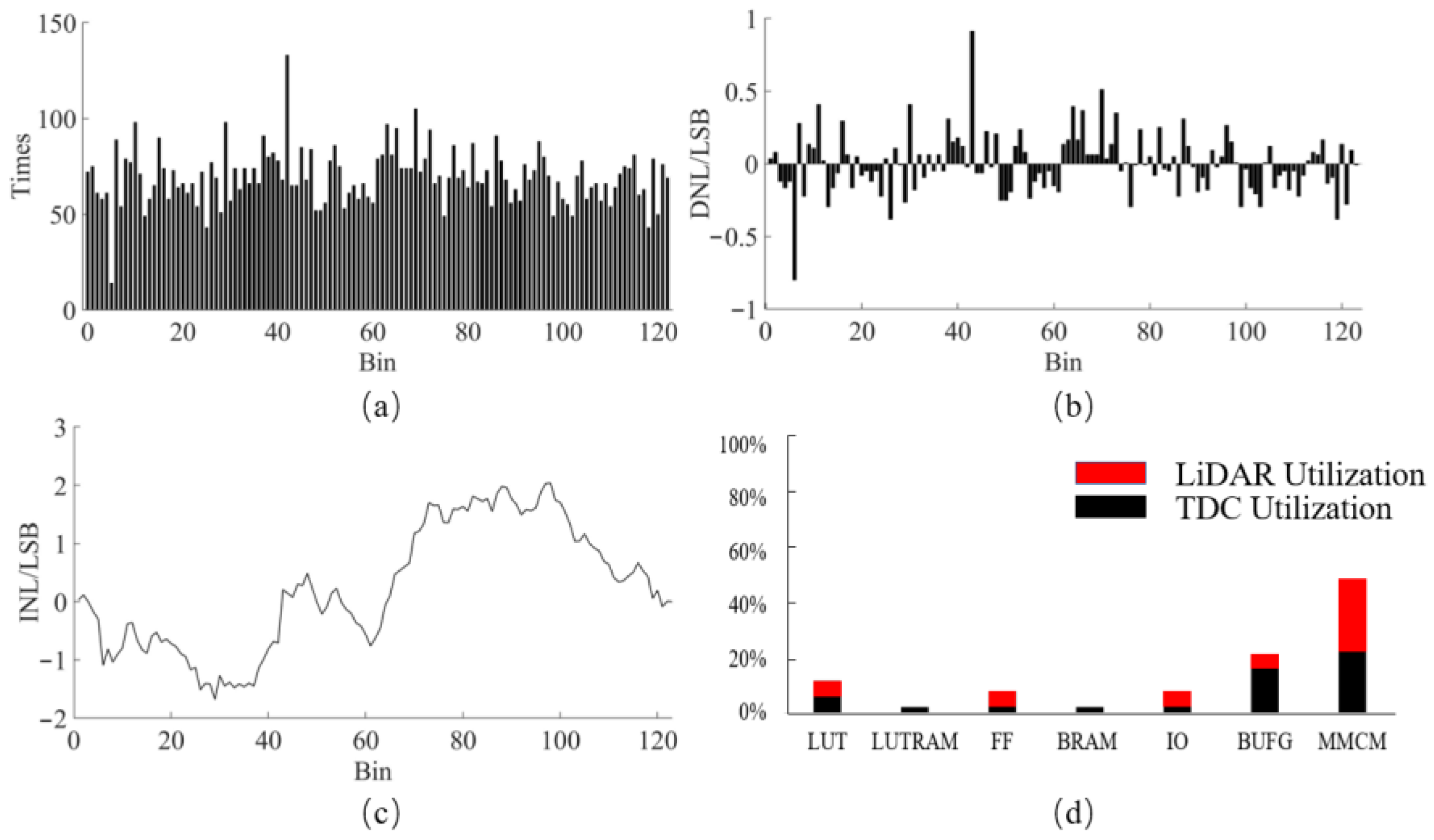
After collecting about 10,000 points, the injection of hit pulses was ceased and the values of each address in RAM were read out by a PC for statistical analysis. The statistical results of each carry series are shown in Figure 7a. The number of counts of the last bin is 123, and most of the bins are distributed around 80 times. After bin-by-bin calibration, the DNL and INL were measured over the entire range of the delay line in the TDC and obtained through the code density test. The results are shown in Figure 7b,c; the DNL is within 1 LSB, and the INL is within 2.5 LSB. Most of the bins are in the normal range; only bin 5 and bin 42 exhibit unequal distribution in the TDC bins. The DNL is mainly caused by the chip structure, clock distribution, routing, and temperature, which leads to unequal bin widths in the delay line. The unequal bin widths affect the measurement accuracy in intelligent sensor equipment such as LiDARs. The error can be partially compensated and calibrated by INL calibration to obtain higher time measurement accuracy. In addition, too much resource utilization in an FPGA has an adverse effect on the layout and wiring inside, which brings more instability to the system. After synthesis and implementation, the source utilization in the FPGA is summarized in Figure 7d. The implementation of the proposed TDC utilizes 6% of the LUT as a function generator, 2% of the LUTRAM as a shift register, 6% of the flip-flops, and 6% of the IO port. The average resource utilization of the TDC is 7%. The implementation of the 2-D LiDAR, which will be elaborated on in the next section, utilizes 6% of the LUT, 2% of the flip-flops, and 2% of the IO port. The average resource utilization of the LiDAR and total architecture are 8% and 15%, respectively. The resource utilization in full configuration is organized in Table 1, where only 2112 DFFs, 1056 LUTs, and 8 IO ports are used. These data demonstrate the low resource utilization of the proposed TDC. Table 2 shows the power consumption of the FPGA-TDC, and little power is consumed. The total on-chip power is 0.288 W. The dynamic power is 0.193 W, and the device’s static power is 0.095 W. The ultra-low resource utilization in FPGA demonstrated the potential implementation in more low-end FPGAs such as Spartan6 and Cyclone IV.
Compared with some of the previously published works using TDL methods, our FPGA-TDC is characterized by lower resource cost, as shown in Table 3.

4. FPGA-Based LiDAR

4.1. Laser Driver Circuit

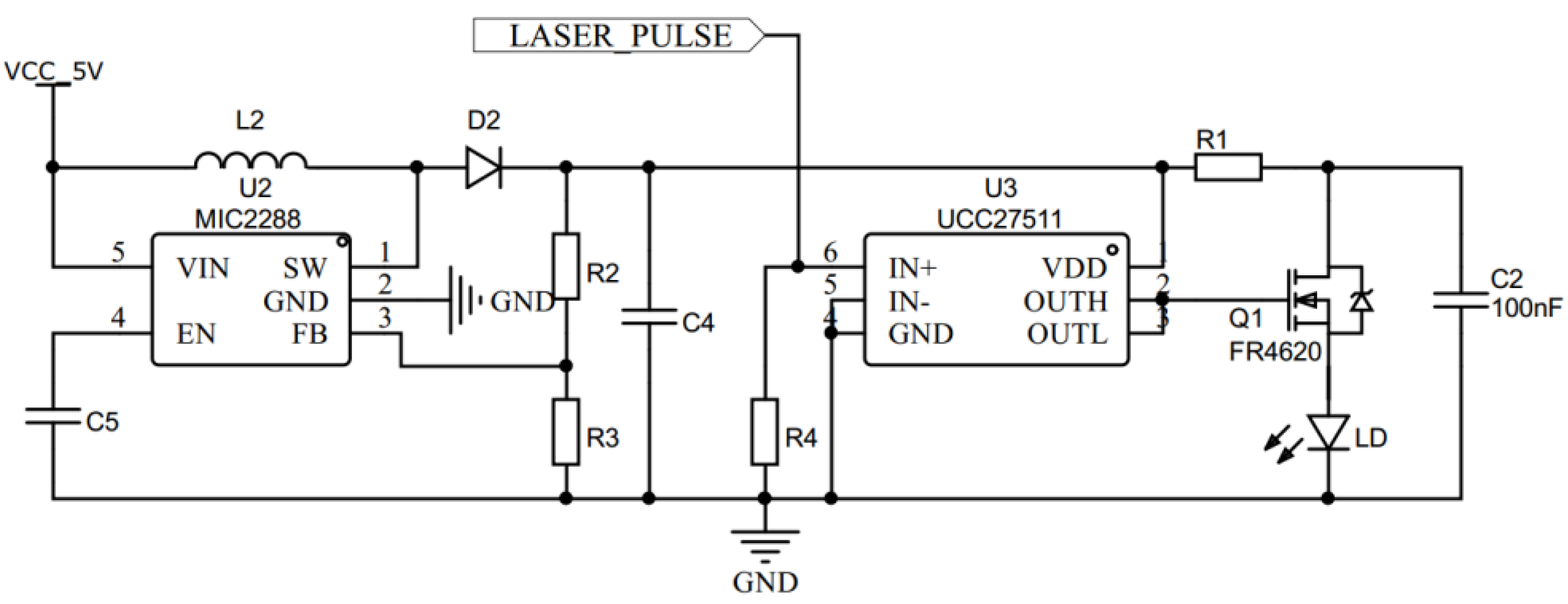
A pulsed laser diode (LD) has the advantages of small volume, high peak power, and high conversion rate. The schematic of the driver circuit is shown in Figure 8; the SPL PL90-3 at 905 nm wavelength from Osram, Munich, Germany is adopted as the laser diode. To obtain a large peak power, the LD requires a short trigger and energy storage. The short trigger with a pulse width of about 30 ns is generated inside the FPGA using the digital synthesis technique. The specific approach is to maintain the duration of the pulse through the counter. Energy is stored and released through a 100 nF energy-storage capacitor. To realize charging and discharging in a short time, a high-speed fast shutdown MOSFET FR4620 from Infineon, Munich, Germany is adopted to rapidly control the capacitor. In Figure 8, the LASER_PULSE is the laser pulse signal input, which is used for the MOSFET switching signal. C 2 is the energy-storage capacitor, which releases instantaneous high peak current pulse for the laser diode through the MOSFET. To realize the high-speed switching function, the MIC2288 is adopted to build a boost circuit to improve the operating voltage, and UCC2751x is adopted to drive the MOSFET power switch effectively. The operating voltage is adjusted by changing the values of the feedback resistor R 2 and R 3 values. According to the formula of capacitor voltage change and output current, the value of storage capacitance can be calculated by the following equation [35]:
  I P × t p = C × U
where C represents the value of the energy storage capacitor. The increase in the value of C will affect the working voltage U, the width of the current pulse t p , and the peak amplitude current I P . When the operating voltage is 12 V and the pulse width is 30 ns, the peak amplitude of the pulse current reaches 35 A, corresponding to a 70 W peak power of the laser pulse. The circuit power is supplied by 5 V DC voltage, which can be provided by the PC USB interface.

4.2. Receiver Circuit

The laser receiver is a key module of LiDAR; it converts the returned optical signal to the electrical signal, provides gain amplification for the electrical signal, and discriminates the arrival time of the returned pulse signal. The circuit schematic is depicted in Figure 9a; the receiver circuit adopts a high gain avalanche photodiode (APD, AD500-9 from Osram, Munich, Germany) to convert the collected optical signal to the photocurrent. The AD500-9 has a fast rise time, low noise, and a high responsivity of 60 A/W at 905 nm wavelength [36]. Due to the weak power of the laser pulses reflected from the target surface, a high reverse bias voltage of about 200 V is required to generate avalanche gain. High reverse voltage is provided by the DC–DC boost circuit shown in Figure 9b. The MAX1771 is the step-up DC–DC controller, using the current-limited pulse-frequency modulation (PFM) control scheme. The voltage can reach sufficient amplitude for APD by selecting two appropriate resistors R 1 and R 2 as follows:
R 2 = R 1 × V A P D _ V V R e f 1
where the V R e f is 1.5 V; the APD voltage is determined by the ratio of R 1 and R 2 . To obtain a voltage of 200 V, R 1 and R 2 are set to 20 kΩ and 2.6 MΩ, respectively, which will improve the sensitivity of the APD. The photocurrent generated from the APD is then amplified by the integrated transimpedance amplifier (TIA, MAX3658 from Maxim, California, U.S.). The function of D 1 is to protect the TIA from ESD. The MAX3658 features an 18 kΩ transimpedance gain and 580 MHz bandwidth, which can convert the weak signal received by APD from the current into a voltage signal for further processing. It has a differential output to effectively suppress common-mode noise. The differential signal outputs from TIA are used as the differential input for the high-speed comparator ADCMP600 through two capacitors to isolate the DC signal. The ADCMP600 is used to discriminate the arrival time of the returned pulse. The trigger signal from the comparator is obtained through the LASER_RECEIVE port, which is used as the stop signal for the time counting in TDC.

4.3. Transceiver and LiDAR

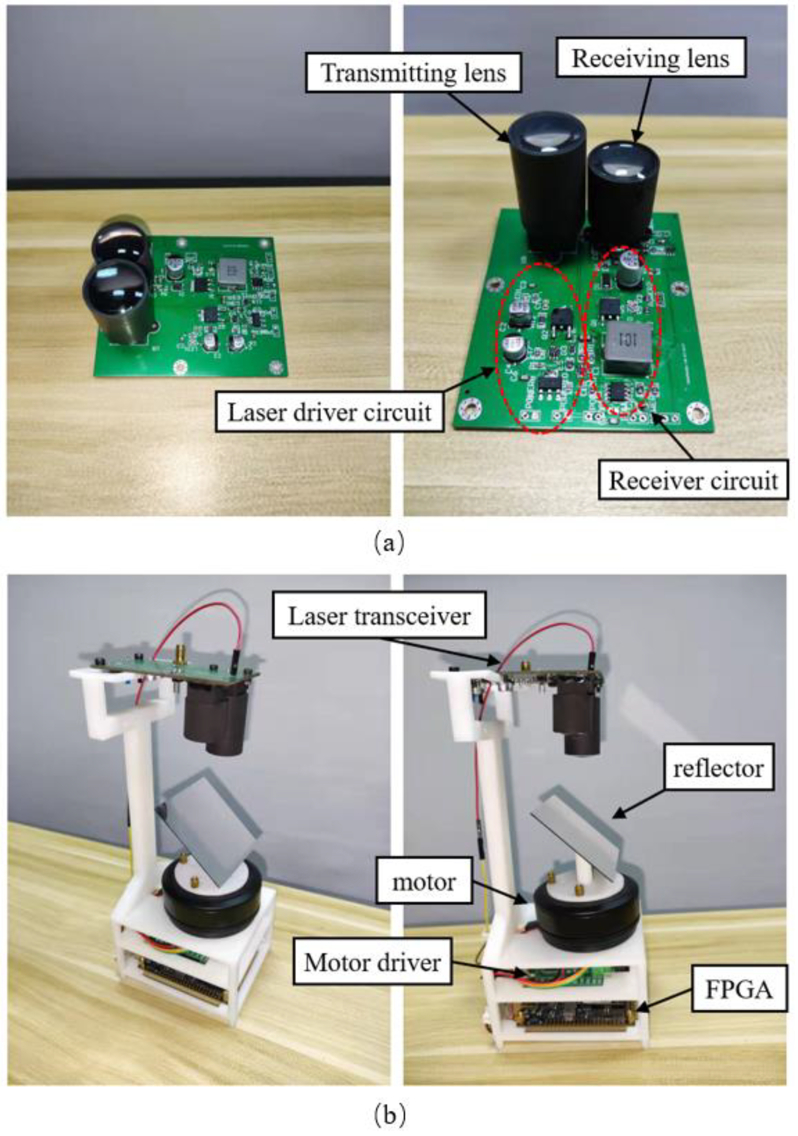
The printed circuit board (PCB) of the transceiver module is demonstrated in Figure 10a. It has a size of approximately 77 mm × 80 mm. The lenses on the board are used to collimate the emitted laser beam and focus the returned laser on the surface of the APD, improving the detection efficiency. The long one is the transmitting lens, which is used to collimate the laser beam emitted by LD, and the short one is the receiving lens, which is used to focus the reflected light received by APD. The focal length of the transmitting lens and receiving lens are respectively 38 mm and 28 mm, which are fixed by mounts fabricated in a symmetrical structure. Symmetrical transmitting and receiving lenses allow for more accurate measurement. The laser transmitting and receiving circuits are integrated into this module, and both are powered by the 5 V DC power supply. The 5 V DC power supply is also shared by all components in the LiDAR prototype to reduce strict requirements for power supply.
As demonstrated in Figure 10b, the LiDAR system proposed mainly consists of a motor, a reflector, an FPGA controller, and a laser transceiver module. The system adopts a mechanical rotation structure, using one motor with a reflector on its surface. The reflector is tilted 45 degrees to the motor plane. The motor contains an encoder chip inside, through which the current angle of the reflector can be read out by the FPGA through the I2C bus. The operations of this system including pulse control, motor control, angle acquisition, and TOF calculation, are processed by the FPGA through I/O ports in real time. With the high-speed rotation of the motor, the whole system can achieve a large horizontal scanning field to form a 2-D LiDAR. The rotation speed of the motor is fixed at five rounds per second, and it takes 0.2 s for a full 2-D scan. The timing and angle data are combined by the FPGA and transmitted to the PC through USB serial protocol for visualization and further processing on the computer. Two of the IO ports of the FPGA are used as the TX and RX ports. It is necessary to be noted that the demonstrated LiDAR is a prototype; the FPGA core board adopted in the LiDAR can be replaced by a single chip, which would be further integrated into the transceiver board to achieve more compact dimensions. The whole structure can be made more compact by delicately designing the structural parts.

4.4. Experiment Test

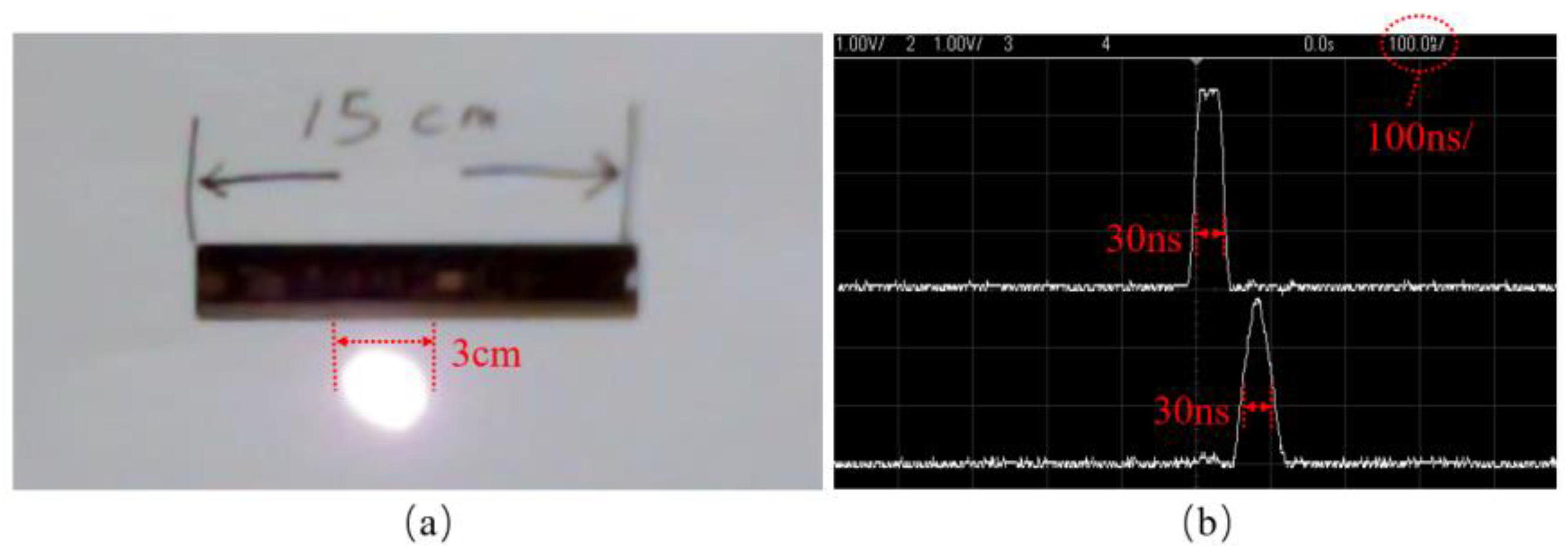
The laser spot size and pulse waveform were tested using an infrared camera and an oscilloscope. Captured by the infrared camera, the laser spot is shown in Figure 11a, where the spot is collimated through a lens with a focal length of 38 mm. The diameter of the laser spot is about 3 cm at a distance of 2 m. In Figure 11b, the FPGA trigger signal (top) and the transmitted pulse signal (bottom) are captured and visualized by the oscilloscope. At the scale of 50 ns, the pulse width of the transmitted signal and the received signal is about 30 ns. The repeated ranging rate of the transceiver module is 12 kHz, and the ranging distance can reach 10 m.
Due to the delays of the components and circuit routes, the TDC data have a measurement error with neglected perturbation, which can be corrected by multiple fixed-point measurements. After several measurements, ranging data of the LiDAR were calibrated and under test at distances of 1.5 m and 3 m, as shown in Figure 12a. For each distance, 2000 points were tested, and nearly all the points are located very close to the true distance, proving the timing and ranging accuracy. The deviation is shown in Figure 12b; most of the points are around the ground truth distance with very little deviation, exhibiting the distance measurement accuracy of around 0.02 m. The ranging test proves a good linear relationship between the ground truth measured distance and TDC timing values.
Next, the targets with complex profiles and a wide-view scanning were tested to verify the ranging and scanning performance for the 2-D LiDAR. In the horizontal direction, the continuous changes of the obstacle edge are good targets for testing the LiDAR. In Figure 13a, the horizontal profile of the object can be distinguished clearly by one scanning. The edge distance difference between the box and wall is clear and sharp. In Figure 13b, an object with continuous shape changes in the horizontal profile was tested. The detail of the target contour is clear and has almost no distortion compared to the image. Moreover, a wide-view scanning was tested; as shown in Figure 13c, the result restores the distance profile of the environment in the image. In addition, the scanning results of a wall corner and the obstacle with a round shape are shown in Figure 13d,e. The distance of each point is shown on the right side of Figure 13. The environment scanning contour is clear without obvious deformation, which verifies the stability and accuracy of the 2-D LiDAR. The scanning tests have fully proved that the LiDAR with FPGA-TDC timing can scan various objects with complex contours well with high accuracy for small distance changes, which proves the stability and continuity of our 2-D LiDAR system.

5. Conclusions

In summary, a digitally integrated 2-D LiDAR system is implemented in a low-end FPGA together with a lightweight and resource-saving TDC based on a symmetrical tapped delay line. The LiDAR employs the ToF ranging method to measure distance. It is built with a homemade transceiver and a mechanical scanning structure with off-the-shelf components. To achieve high digital integration and compact dimensions, the LiDAR system integrates timing, controlling, and data processing logics together in ZYNQ7010 without the need for an MCU. Owing to the lightweight architecture, the average resource utilization of the whole architecture in the ZYNQ7010 is 15%. The scanning results of different targets with complex profiles prove that the ranging of the LiDAR and the timing of the TDC operate well and steadily. This structure greatly reduces the cost and dimensions of LiDAR, which would be of significance in consuming applications. Moreover, with low cost and high integration, the proposed digitally integrated LiDAR would find potential applications in smart cities, including robotic navigation, real-time pedestrian counting, truck overload monitoring, social distance detection, and traffic monitoring applications.

Author Contributions

Conceptualization, J.H. and W.W.; methodology, J.H.; software, J.H.; validation, J.H. and S.R.; investigation, J.H. and S.R.; data curation, J.H. and S.R.; writing—original draft preparation, J.H., W.W. and Q.Y.; writing—review and editing, J.H., W.W. and Q.Y.; supervision, W.W.; project administration, W.W.; funding acquisition, W.W. All authors have read and agreed to the published version of the manuscript.

Funding

This research was funded by the National Natural Science Foundation of China, grant number 61905045, and the Guangzhou Science and Technology Project, grant number 202102010501.

Conflicts of Interest

The authors declare no conflict of interest.

References

  1. Xu, P.; Liu, D.; Shen, Y.; Chen, Y.; Zhang, H.; Ye, Z.; Jiang, C.; Zhou, Y.; Liu, Q.; Liu, C. Design and validation of a shipborne multiple-field-of-view lidar for upper ocean remote sensing. J. Quant. Spectrosc. Radiat. Transf. 2020, 254, 107201. [Google Scholar] [CrossRef]
  2. Li, M.; Hu, Y.; Zhao, N.; Qian, Q. Modeling and analyzing point cloud generation in missile-borne LiDAR. Def. Technol. 2020, 16, 69–76. [Google Scholar] [CrossRef]
  3. Wang, L.; Zhang, Y.; Wang, J. Map-based localization method for autonomous vehicles using 3D-LIDAR. IFAC-PapersOnLine 2017, 50, 276–281. [Google Scholar] [CrossRef]
  4. Onda, K.; Oishi, T.; Kuroda, Y. Dynamic environment recognition for autonomous navigation with wide FOV 3D-LiDAR. IFAC-PapersOnLine 2018, 51, 530–535. [Google Scholar] [CrossRef]
  5. Javanmardi, E.; Javanmardi, M.; Gu, Y.; Kamijo, S. Autonomous vehicle self-localization based on probabilistic planar surface map and multi-channel LiDAR in urban area. In Proceedings of the 2017 IEEE 20th International Conference on Intelligent Transportation Systems (ITSC), Yokohama, Japan, 16–19 October 2017. [Google Scholar]
  6. Behroozpour, B.; Sandborn, P.; Wu, M.; Boser, B. Lidar system architectures and circuits. IEEE Commun. Mag. 2017, 55, 135–142. [Google Scholar] [CrossRef]
  7. Malka, V.; Faure, J.; Glinec, Y.; Rechatin, C. Principle and applications of electron beams produced with laser plasma accelerators. J. Phys. Conf. Ser. 2008, 112, 042029. [Google Scholar] [CrossRef]
  8. Chen, X.; Kong, W.; Chen, T.; Liu, H.; Huang, G.; Shu, R. High-repetition-rate, sub-nanosecond and narrow-bandwidth fiber-laser-pumped green laser for photon-counting shallow-water bathymetric Lidar. Results Phys. 2020, 19, 103563. [Google Scholar] [CrossRef]
  9. Wu, D.; Zheng, T.; Wang, L.; Chen, X.; Yang, L.; Li, Z.; Wu, G. Multi-beam single-photon LiDAR with hybrid multiplexing in wavelength and time. Opt. Laser Technol. 2022, 145, 107477. [Google Scholar] [CrossRef]
  10. Chen, Z.; Fan, R.; Li, X.; Dong, Z.; Zhou, Z.; Ye, G.; Chen, D. Accuracy improvement of imaging lidar based on time-correlated single-photon counting using three laser beams. Opt. Commun. 2018, 429, 175–179. [Google Scholar] [CrossRef]
  11. Palani, L.; Rajagopal, S.; Rao, Y. Area efficient high-performance time to digital converters. Microprocess. Microsyst. 2020, 73, 102974. [Google Scholar] [CrossRef]
  12. Christiansen, J. Picosecond stopwatches: The evolution of time-to-digital converters. IEEE Solid-State Circ. Mag. 2012, 4, 55–59. [Google Scholar] [CrossRef]
  13. Gagnon, H.; Franck, J.; Wisztorski, M.; Day, R.; Fournier, I.; Salzet, M. TARGETED MASS spectrometry imaging: Specific targeting mass spectrometry imaging technologies from history to perspective. Prog. Histochem. Cytochem. 2010, 47, 133–174. [Google Scholar] [CrossRef] [PubMed]
  14. Maatta, K.; Kostamovaara, J. A high-precision time-to-digital converter for pulsed time-of-flight laser radar applications. IEEE Trans. Instrum. Meas. 1998, 47, 521–536. [Google Scholar] [CrossRef]
  15. Caram, J.P.; Galloway, J.; Kenney, J.S. Harmonic ring oscillator time-to-digital converter. In Proceedings of the 2015 IEEE International Symposium on Circuits and Systems (ISCAS), Lisbon, Portugal, 24–27 May 2015; pp. 161–164. [Google Scholar]
  16. Tontini, A.; Gasparini, L.; Pancheri, L.; Passerone, R. Design and characterization of a low-cost FPGA-based TDC. IEEE Trans. Nucl. Sci. 2018, 65, 680–690. [Google Scholar] [CrossRef]
  17. Sui, T.; Zhao, Z.; Xie, S.; Xie, Y.; Zhao, Y.; Huang, Q.; Xu, J.; Peng, Q. A 2.3-ps RMS resolution time-to-digital converter implemented in a low-cost cyclone V FPGA. IEEE Tran. Instrum. Meas. 2019, 68, 3647–3660. [Google Scholar] [CrossRef] [PubMed]
  18. Nogrette, F.; Heurteau, D.; Chang, R.; Bouton, Q.; Westbrook, C.; Sellem, R.; Clément, D. Characterization of a detector chain using a FPGA-based time-to-digital converter to reconstruct the three-dimensional coordinates of single particles at high flux. Rev. Sci. Instrum. 2015, 86, 113105. [Google Scholar] [CrossRef] [Green Version]
  19. Song, J.; An, Q.; Liu, S. A high-resolution time-to-digital converter implemented in field-programmable-gate-arrays. IEEE Trans. Nucl. Sci. 2006, 53, 236–241. [Google Scholar] [CrossRef]
  20. Zhao, L.; Hu, X.; Liu, S.; Wang, J.; Shen, Q.; Fan, H.; An, Q. The design of a 16-channel 15 ps TDC implemented in a 65 nm FPGA. IEEE Trans. Nuc. Sci. 2013, 60, 3532–3536. [Google Scholar] [CrossRef]
  21. Kwiatkowski, P.; Szplet, R. Efficient implementation of multiple time coding lines-based TDC in an FPGA device. IEEE Trans. Instrum. Meas. 2020, 69, 7353–7364. [Google Scholar] [CrossRef]
  22. Dadouche, F.; Turko, T.; Uhring, W.; Malass, I.; Dumas, N.; Normand, J. New design-methodology of high-performance TDC on a low cost FPGA targets. Sens. Transducers 2015, 193, 123–134. [Google Scholar]
  23. Wang, J.; Liu, S.; Shen, Q.; Li, H.; An, Q. A fully fledged TDC implemented in field-programmable gate arrays. IEEE Trans. Nucl. Sci. 2020, 57, 446–450. [Google Scholar] [CrossRef]
  24. Lusardi, N.; Garzetti, F.; Geraci, A. Digital instrument with configurable hardware and firmware for multi-channel time measures. Rev. Sci. Instrum. 2019, 90, 055113. [Google Scholar] [CrossRef] [PubMed]
  25. Xia, X.; Ye, M.; He, J. A novel TDC/ADC hybrid reconstruction ROIC for LiDAR. IEICE Electron. Express 2019, 16, 20181076. [Google Scholar] [CrossRef] [Green Version]
  26. Seo, H.; Yoon, H.; Kim, D.; Kim, J.; Choi, J. A 36-Channel SPAD-Integrated Scanning LiDAR Sensor with Multi-Event Histogramming TDC and Embedded Interference Filter. In Proceedings of the 2020 IEEE Symposium on VLSI Circuits, Honolulu, HI, USA, 16–19 June 2020. [Google Scholar]
  27. Lesani, A.; Nateghinia, E.; Miranda-Moreno, L.F. Development and evaluation of a real-time pedestrian counting system for high-volume conditions based on 2D LiDAR. Transp. Res. Part C Emerg. Technol. 2020, 114, 20–35. [Google Scholar] [CrossRef]
  28. Tai, T.S.; Zuo, H.; He, S. 3D LIDAR based on FPCB mirror. Mechatronics 2022, 82, 102720. [Google Scholar] [CrossRef]
  29. Seferiadis, G.; Pouchet, M.; Gough, M. FPGA implementation of a delay-line readout system for a particle detector. Measurement 2006, 39, 90–99. [Google Scholar] [CrossRef]
  30. Lusardi, N.; Los, J.; Gourgues, R.; Geraci, A. Photon counting with photon number resolution through superconducting nanowires coupled to a multi-channel TDC in FPGA. Rev. Sci. Instrum. 2017, 88, 035003. [Google Scholar] [CrossRef] [Green Version]
  31. Machado, R.; Cabral, J.; Alves, F.S. Recent developments and challenges in FPGA-based time-to-digital converters. IEEE Trans. Instrum. Meas. 2019, 68, 4205–4221. [Google Scholar] [CrossRef]
  32. Maamoun, M.; Arami, S.; Beguenane, R.; Benbelkacem, A.; Meraghni, A. A 3 ps resolution time-to-digital converter in low-cost FPGA for laser rangefinder. Proc. World Congr. Eng. 2017, 1, 7–11. [Google Scholar]
  33. Chen, P.; Hsiao, Y.; Chung, Y. A high resolution FPGA TDC converter with 2.5 ps bin size and -3.79~6.53 LSB integral nonlinearity. In Proceedings of the 2016 2nd International Conference on Intelligent Green Building and Smart Grid (IGBSG), Prague, Czech Republic, 27–29 June 2016. [Google Scholar]
  34. Prasad, K.; Chandratre, V.; Sukwani, M. An FPGA based 33-channel, 72 ps LSB time-to-digital converter. Nucl. Instrum. Methods Phys. Res. A 2022, 1027, 166052. [Google Scholar] [CrossRef]
  35. OSRAM Opto Semiconductors, SPL PL90_3_EN Datasheet, Radial T1 3/4. Available online: https://dammedia.osram.info/media/resource/hires/osram-dam-6189135/SPL%20PL90_EN.pdf (accessed on 11 July 2018).
  36. First Sensor APD Data Sheet, Part Description AD500-9 SMD, Order # 501122; 501818, Version 20-06-11. Available online: https://www.first-sensor.com/cms/upload/datasheets/AD500-9_SMD_3001495.pdf (accessed on 11 June 2020).
Figure 1. Architecture of delay line.
Symmetry 14 01256 g001
Figure 2. (a) CARRY4 elements in Xilinx FPGA; (b) delay line structure.
Symmetry 14 01256 g002
Figure 3. Fine and coarse time measurements.
Symmetry 14 01256 g003
Figure 4. Input filter schematic and simulation result.
Symmetry 14 01256 g004
Figure 5. (a) Block diagram of TDC and average LSB simulation; (b) TDC timing simulation.
Symmetry 14 01256 g005
Figure 6. Code density statistics diagram.
Symmetry 14 01256 g006
Figure 7. (a) Statistical analysis of the TDC bins; (b) DNL; (c) INL; (d) FPGA resource utilization.
Symmetry 14 01256 g007
Figure 8. Laser drive circuit.
Symmetry 14 01256 g008
Figure 9. (a) Receiver circuit. (b) Bias voltage circuit.
Symmetry 14 01256 g009
Figure 10. (a) Laser transceiver module. (b) The prototype of the 2-D LiDAR system.
Symmetry 14 01256 g010
Figure 11. (a) Laser spot. (b) The waveforms of the trigger signal and transmitter pulse.
Symmetry 14 01256 g011
Figure 12. Ranging test. (a) Distance test of 1.5 m and 3 m; (b) Deviation test of 1.5 m and 3 m.
Symmetry 14 01256 g012
Figure 13. Scanning results. (a) Continuous object scanning; (b) Discontinuous object scanning; (c) Wide-view scanning; (d) Rectangular object scanning; (e) Circular object scanning.
Symmetry 14 01256 g013
Table 1. The TDC resource utilization.
ResourceUsedUtilization
LUTs10566%
DFFs21126%
IO86%
Table 2. Power consumption.
NameConsumption
Dynamic0.193 W
Clocks0.029 W
Signals0.038 W
Logic0.031 W
MMCM0.095 W
I/O<0.001 W
Total0.288 W
Table 3. Comparison of resource utilization.
WorkUtilization (LUTs, DFFs)
This paper1056, 2112
[24]3837, 7010
[21]>2000, >2000
Publisher’s Note: MDPI stays neutral with regard to jurisdictional claims in published maps and institutional affiliations.