
Inorganic Thin-Film Solar Cells: Challenges at the Terawatt-Scale


Ordine Regionale dei Chimici della Campania, Via A. Tari 22, 80138 Naples, Italy
Symmetry 2023, 15(9), 1718; https://doi.org/10.3390/sym15091718
Submission received: 31 July 2023
/
Revised: 21 August 2023
/
Accepted: 30 August 2023
/
Published: 7 September 2023
Abstract
:Thin-film solar cells have been referred to as second-generation solar photovoltaics (PV) or next-generation solutions for the renewable energy industry. The layer of absorber materials used to produce thin-film cells can vary in thickness, from nanometers to a few micrometers. This is much thinner than conventional solar cells. This review focuses on inorganic thin films and, therefore, hybrid inorganic–organic perovskite, organic solar cells, etc., are excluded from the discussion. Two main families of thin-film solar cells, i.e., silicon-based thin films (amorphous (a-Si) and micromorph silicon (a-Si/c-Si), and non-silicon-based thin films (cadmium telluride (CdTe) and copper–indium–gallium diselenide (CIGS)), are being deployed on a commercial scale. These commercial technologies, until a few years ago, had lower efficiency values compared to first-generation solar PV. In this regard, the concept of driving enhanced performance is to employ low/high-work-function metal compounds to form asymmetric electron and hole heterocontacts. Moreover, there are many emerging thin-film solar cells conceived to overcome the issue of using non-abundant metals such as indium (In), gallium (Ga), and tellurium (Te), which are components of the two commercial thin-film technologies, and therefore to reduce the cost-effectiveness of mass production. Among these emerging technologies are kesterite CZTSSE, intensively investigated as an alternative to CIGS, and Sb2(S,Se)3. In this review, after a general overview of the current scenario of PV, the three main challenges of inorganic thin-film solar cells, i.e., the availability of (safe) metals, power conversion efficiency (PCE), and long-term stability, are discussed.
1. Introduction
Sustainable development is defined as “development that meets the needs of the present without compromising the ability of future generations to meet their own needs” [1].
However, scientific research often addresses specific, single, isolated goals without a large vision of more general and global goals, resulting in new problems. An example is given by the Aswan Dam, built between 1960 and 1970 with the aim of producing hydroelectric energy: it resulted in increased water salinity with a consequent migration of marine fauna, reduced fishing productivity, and reduced soil fertility downstream of the dam, causing food supply problems for the people.
Since the Industrial Revolution, the main energy sources have been coal, oil, and natural gas, which are responsible for the dramatic increase in global greenhouse gas emissions, with all its negative consequences. The world has to face two urgent challenges. The first, proposed by the COP26 summit, is to keep “1.5 degrees alive”—that is, to ensure the world remains committed to preventing global heating from exceeding more than 1.5 degrees above pre-industrial levels [2]. The second concerns the 28 TW global energy demand foreseen for 2050 [3]. Both these challenges make a sustainable energy supply necessary.
2. The Rise of Inorganic Thin-Film Solar Cells
PV directly converts solar energy into electricity and therefore offers a sustainable answer to the increasing global energy demand. The solar PV industry has evolved remarkably. Milestones in the field are reported in Figure 1.
PV is the main source of new power capacity in many countries such as China, Japan, India, and the USA. In Figure 2, the global PV module production and cumulative installed PV capacity are reported. In 2010, Asia produced 82% of the total global production, which, in 2020, increased to about 92%. In 2020, China produced about 97 GW for 67% of the global module production [4]. This trend is a consequence of the decreasing price of PV systems: the cost of PV-produced electricity has been levelized to the so-called point of socket parity, which refers to the moment when the levelized cost of electricity (LCOE) of solar electricity becomes lower than the retail price of electricity.
In order to meet a considerable portion of the global energy demand foreseen for 2050, i.e., 28 TW [3], the installed capacity of solar PV will have to expand at least to 5TW. However, material or resource constraints are a relevant issue for the future of PV technologies in large-scale applications. China is the largest global supplier for critical raw materials (CRMs), i.e., those that have high economic importance and a high supply risk (Table 1): this leading role is strictly related to its higher percentage of production and installation of PV modules compared to other countries (Figure 2).
Many of CRMs listed in Table 1 are used in the production of PV panel modules. Crystalline silicon (c-Si) wafer panels are first-generation solar PV panels and account for about 95% of the total production in 2020. In particular, in 2020 the share of mono-crystalline Si technology in the total c-Si production (compared to multi-crystalline one) was about 84%, vs. 66% recorded in 2019 [4]. c-Si is more affordable and highly efficient compared to other materials, thanks to the economies of scale of silicon (its main material), making it difficult for other technologies to compete.
Thin-film technologies are often referred to as second-generation solar PV. Typical thin-film solar cells use only a few microns of active material compared to hundreds of microns used for a wafer-based cell. There are two main groups of thin film technologies. Silicon-based thin film based on amorphous (a-Si) and micromorph silicon (a-Si/c-Si) is the first.
The second is non-silicon-based thin film technology. Among non-silicon-based thin film technologies, there are CdTe and CIGS, which are fully inorganic-material-based [6,7,8] and perovskites. The term perovskite refers to the inorganic salt CaTiO3 and any structure adopting the same ABX3 three-dimensional (3-D) structural framework. However, in the case of perovskite materials for solar cells, the adjective perovskite refers to organic−inorganic hybrid perovskites, in the general formula ABX3, with at least one of the “A”, “B”, or “X” ions being organic. Typically, the “A” cation is organic while “B” is a metal and “X” is a halogen (Cl, Br, or I), e.g., CH3NH3Pb(I,Cl,Br)3 or CH(NH2)2SnI3, which employs methylammonium (CH3NH3+) and formamidinium (NH2CH=NH2+) “A” cations, respectively. Even though perovskites are promising, they still face some significant challenges. One is durability: they need to be protected from moisture through encapsulation, for instance by an aluminum oxide layer or sealed glass plates; another challenge concerns the discrepancy between the high efficiency levels obtained at a small scale and those obtained with larger cell areas; last but not least is the presence of toxic lead components which produce toxic waste from the precursor solution during manufacturing [9].
Even though perovskites have shown a more rapid increase in efficiency (from 3.8% in 2009 to 25.5% in 2020) compared to CdTe and CIGS, the prospect of their commercialization still remains unachievable. Perovskites will not be discussed in this review, which is focused on inorganic thin film solar cells. Currently, CdTe thin film technology has penetrated into the market, while CIGS is also on the market (Figure 3). Other new emerging technologies discussed below, such as CZTSS, are at the prototype level [10].
The cost of silicon rose around the years 1988 and 2006 owing to its increased demand, resulting in increased interest for more economic, even though low efficient, thin-film technology for large-scale power generation (Figure 4). However, a different trend occurred a few years later, in 2012, i.e., the production shifted towards c-Si technology due to the falling silicon prices, whilst the overall market share of thin-film technologies was constantly decreasing (Figure 4).
In 2020, the production in GWp was 7.7, 23.3 and 120.6 for thin film, multi-Si, and mono-Si, respectively [4]. Despite the high efficiency level of this first-generation PV technology, there is room for improvement, such as by (i) lowering the cost of c-Si modules; (ii) reducing metallic impurities, grain boundaries, and dislocations; (iii) reducing waste to mitigate environmental effects; and (iv) yielding thinner wafers [11].
However, even though the overall market share of thin-film technologies has been decreasing constantly in the last years, these technologies present additional advantages beyond the use of less material for the absorber layer. In order to investigate the environmental performance of PV systems accurately, a life cycle assessment (LCA) is usually conducted. The two most widely used environmental indicators are energy payback time (EPBT) and greenhouse gas (GHG) emission rate [12,13]. Peng et al. [13] carried out a thorough review of the LCA studies of five common PVsystems, i.e., mono-Si, multi-Si, a-Si, CdTe, and CIGS thin film, and some advanced PV systems. The results show that, among the five common PV systems, the CdTe PV system is the most promising in terms of EPBT and GHG emission rate (Table 2). The environmental issue of CdTe cells concerning the risk of releasing carcinogenic elemental cadmium has been addressed well by Romeo and Artegiani [7].
Thin-film PV systems showed EPBT and GHG emission rates within the range of 0.75–3.5 years and 10.5–50 g CO2-eq/kW h, respectively, whilst the EPBT of mono-Si PV systems ranged from 1.7 to 2.7 years with GHG emission rates from 29 to 45 g CO2-eq./kW h, with the worst values of the sustainable indicators due to the energy intensity during the production process [13]. Below, the three main challenges of inorganic thin-film solar cells, i.e., the availability of (safe) metals, power conversion efficiency (PCE), and long-term stability, are discussed.
3. The Challenges
3.1. Availability of Safe Raw Materials
The use of reduced materials while maintaining performance is desirable in any technological application. In the three thin-film PV technologies currently on the market, i.e., CdTe, CIGS, and a-Si, the clear advantage is that the weight of the electrical active component is so low that the panel weight is dominated by the glass substrate, encapsulation materials, and other components necessary for structural integrity. The wiring, junction boxes, inverters, and mounting structures are similar in all commercialized solutions. Moreover, another advantage relies on the fact that the active material can be deposited onto flexible surfaces, making the solar cells versatile. Thin-film panels have been investigated for several applications, such as commercial and industrial rooftop installations, ground-based solar farms, recreational vehicles, and camping. In recent years, research interest in portable and wearable power sources for flexible electronics such as sensors and telecommunication devices has emerged [14]. However, at the terawatt scale, as mentioned above in the introduction, the deployment of any of the three thin-film technologies requires massive amounts of natural resources, including electricity and materials. The limited supplies of these resources will prevent them from reaching terawatt scales. In the case of silicon-based thin film, the limitation concerns relevant energy amounts and Ag used as the contact. The low availability of Te in CdTe and In and Ga in CIGS are limitations for large scale thin-film PV [6,7,8,15,16] (Figure 5).
CIGS cells have achieved high efficiency levels (23.6%), comparable to those of commercial crystalline silicon [4]. However, manufacturing CIGS cells can be difficult due to the rarity of indium, as well as to the complex stoichiometry and multiple phases needed to produce them, restricting large-scale production in the near term [17,18]. Indium, as well as cadmium, are hitchhiker elements, i.e., critical elements that are mainly not produced in their own right, but are instead by-products of, or ‘hitchhikers’ on, extraction from primary or ‘attractor’ metal deposits [19] (Table 3). Therefore, the lifetimes of Ga, Ge, In, and Te, which are hitchhikers on the production of Zn, Al, and Cu, are limited by the production timescales of the main (base) metals.
CdTe cells achieved an efficiency of 22.3%, very similar to that of CIGS, and were characterized by good absorption and low energy losses [4,7]. Historically, there are two large categories of CdTe PV devices on the basis of substrate deposition temperature: low temperature (<450 °C) and high temperature (>450 °C). Low substrate temperature (LST) CdTe makes production very flexible and affordable thanks to lower energy consumption, lower substrate stress, a larger choice of substrates, and the possibility of substituting glass with polymers for flexible solar devices [7]. CdTe currently has the largest market share of all thin-film technologies [18] (Figure 6).
CdTe panels have the lowest carbon footprint, but they contain cadmium, a toxic element, requiring special precautions to be taken during manufacture, installation, and disposal [7]. The Restriction of Hazardous Substances (RoHS) impacts the entire electronics industry, and many electrical products as well [21]. Among the ten restricted substances for which RoHS specifies maximum levels, there are Cd and Pb. These metals are classified as materials having adverse impacts on the environment [22] and as type-I carcinogens by the International Agency for Cancer Research (IARC) [23]. Moreover, tellurium, like indium, is a hitchhiker element on the production of Cu, as mentioned above. In and Te, like Ge and Ga and other critical elements, come mainly from China, as mentioned above (see Table 1). When a single nation has a monopoly on the supply of a particular resource, questions arise over how secure this might prove in the longer term. The recent conflict in Ukraine, with gas supplies cut off from Russia to several European countries, gives a remarkable example of the matter and brings more awareness to global interconnections and the need for long-term thinking.
Possible Solutions
Possible options to overcome the issue of rising demand for a given hitchhiker are: (i) the expansion of the rate of production of the major attractor metal, which for Te and In are Cu and Zn, respectively (Table 3); (ii) substitution with alternative materials; (iii) the improvement of the extraction efficiency of the minor by-product from the base metal ore; and (iv) finding alternatives, and above all independent sources of the critical metals. The first option in the case of Te and In concerns the production of Cu and Zn. Currently, both these elements are not abundant (Figure 5) at different levels: Cu has “limited availability, future risk of supply” and zinc shows “serious threat in the next 100 years” (Figure 7).
Energy requirements may prove prohibitively high for the practical recovery from low grade ores of elements and metals such as copper and zinc that were initially recovered from concentrated mines.
By way of the second option listed above, i.e., the substitution strategy, many efforts have been made to eliminate the use of In and Ga. The complete replacement of In with Zn and Ga with Sn have given rise to kesterite-based materials, including Cu2ZnSnS4 (CZTS), Cu2ZnSnSe4 (CZTSe), and Cu2ZnSn(S,Se)4 (CZTSSe), which emerge as potential replacements not only of CIGS, but also of CdTe absorbers [25,26,27,28,29,30]. Because CZTS, CZTSe, and CZTSSe solar cells are composed of low-cost and Earth-abundant elements, they have the advantage of large-scale production ability compared with CIGS solar cells. Kesterite CZTSSe has been recognized as a prospective alternative absorber material due to its controllable bandgap (Eg) (1.0 to 1.5 eV) and high absorption coefficient (more than 104 cm−1). It should be noted that Eg of the CZTSSe absorber can be controlled by varying the S/(S + Se) ratio from ~1.0 eV of Cu2ZnSnSe4 (CZTSe) to ~1.5 eV of Cu2ZnSnS4 (CZTS [31,32,33,34,35]. The efficiency of CZTSSe solar cells has raised from ~12.6% [35,36] to 13.6% [37]. Some issues related to CZTSSe are discussed below.
Bismuth, which is termed a “green heavy metal” [38], is a potential candidate to replace toxic heavy metals such as Cd and Pb in photosensitizers, thus lowering the environmental toxicity. Ternary compounds such as AgBiS2 containing Bi have been recently explored as eco-friendly materials. Since 2016, AgBiS2, initially utilized as a counter electrode material [39] in quantum dot solar cells because of its excellent electrochemical properties, has been extensively studied in PV. The ideal low bandgap (1–1.32 eV) of AgBiS2 enables light absorption in both the visible and infrared regions. Recently, it has been found that bismuth-based nanocrystals do not only consist of non-toxic elements relatively abundant in nature, but are also cheap to produce [40]. New, ultra-thin solar cells (30 nm thick, i.e., 10 to 50 times thinner than current thin-film PV) made from cation-disorder-engineered AgBiS2 colloidal nanocrystals offer an absorption coefficient that is higher than other PV materials, enabling highly efficient, extremely thin absorber PV devices [40].
Antimony chalcogenides, Sb2(S,Se)3 (SbSSe), have attracted attention over the last few years as a light-harvesting material for PV technology owing to their phase stability, earth abundancy, and low toxicity. However, the lack of a suitable material processing approach to obtain SbSSe films with optimal optoelectronic properties and morphology severely hampers prospects for efficiency improvement. Recently, a new approach to deposit high-quality SbSSe films has been demonstrated [41], highlighting the potential of SBSSe as an emerging PV material, as discussed below.
Regarding the third and fourth options mentioned above, i.e., the improvement of the extraction efficiency of the minor by-product from the base metal ore, and finding alternatives and independent sources of the critical metals, current advanced research works have proposed innovative and environmentally sustainable methods, which are suitable for both the extraction (by increasingly poor, complex, and difficult-to-reach raw materials) and their downstream processing [42]. Bioleaching (or biomining) is a process in mining and biohydrometallurgy (natural processes of interactions between microbes and minerals) that extracts valuable metals from a low-grade ore with the help of microorganisms such as bacteria or archaea [43]. Although biomining may not fit the common mining stereotype, actually, the same biological process had been unknowingly used to extract metals at mine sites in, for example, Spain, the UK and China, for several hundred years [44,45,46]. The ‘new’ biotechnology was established in the 1960s by the Kennecott Copper Corporation to extract copper from waste rock dumps at the Bingham Canyon mine in Utah, and later at the Chino mine in New Mexico [47,48]. Rather than using heat to extract the metals from the rocks, biomining uses microbes. Up to now, biomining has been mainly used to extract copper and gold from rocks where they are present at low concentrations (around 0.5% or less), known as low-grade ores, which otherwise would require more energy-intensive heat-based methods, which are not cost effective, such as smelting. Around 5% of the world’s supply of gold and 20% of its copper is currently extracted using biomining, which is being used to extract more metals from more materials in more places and is often more effective than traditional mining applications, and can even be used to clean mine tailings sites [49].
3.2. Power Conversion Efficiency (PCE)
Efficiency is a key metric in the development of PV because the cell cost is only a small fraction of the total cost of a solar power generation system (Figure 8).
Therefore, increasing efficiency is a near-linear driver for reducing the cost of PV electricity per kilowatt-hour [50].
The conversion efficiency of light into electrical power is defined as the ratio of the output electricity to the input energy of sunlight. In practice, the PCE (η) of a solar cell is defined as the ratio of the maximum power output, Pmax, generated by the solar cell to the power input, Pin, based on the measurement of current density and voltage (I-V) curve (Figure 9) [51]:
where Jmp and Vmp are the current density and voltage at the maximum power point (see Figure 9), Jsc is the short circuit current density, Voc is the open circuit voltage, and FF is the fill factor. FF, which has been introduced to simplify the calculation of the efficiency, is defined as the ratio of the areas of the two rectangles determined by Jmp and Vmp (blue in Figure 9) and by Voc and Jsc (green in Figure 9), respectively.
Accordingly, the three parameters of Voc, Jsc, and FF combine to compute the efficiency of a device. The efficiency of a solar cell has fundamental limits, as determined by Shockley and Queisser (S-Q), who calculated a maximum efficiency using a single p-n junction of 32% for c-Si solar cells (Shockley W. and Queisser, 1961). With modern approaches such as tandem cells, the efficiency is 45% [52]. In real solar cells, not all incident light is absorbed in the semiconductor layer and not all generated carriers are collected. Therefore, Jsc is below the maximum value that can be achieved for a given band gap. Voc is also reduced below the S-Q value by phenomena such as Auger recombination, band tail recombination, and recombination at bulk, interface, and surface defects [53,54,55]. Moreover, FF is reduced by resistance, contact losses, and other nonidealities. Therefore, combining all these factors, real efficiencies are lower than the S-Q limit for a given band gap (Figure 10).
Aside from the significant development in hybrid materials such as organic-inorganic perovskite, high efficiency commercial inorganic thin-film materials, like CdTe [7], CGIS [6] has made important steps forward in the past few years (Figure 10 and Table 4).
The record lab cell efficiency results of mono-crystalline and multi-crystalline silicon wafer-based technology were 26.7% (Table 4, entry 1) and 24.4% (Table 4, entry 2), respectively. The highest lab efficiency results in thin-film technology were 23.6% for CIGS and 22.3% for CdTe solar cells (Table 4, entries 4 and 5, respectively).
Regarding module efficiency, CIGS and CdTe (Table 4, entries 4 and 5, respectively) are now approaching the multi-crystalline silicon efficiencies (Table 4, entry 2).
Common to thin-film CIGS, CdTe, and a-Si in the decade between 2000 and 2010 was the effort devoted to increasing manufacturing, which resulted in a reduced rate of cell efficiency increase. Industry during this time focused on tighter process control and finer understanding to replicate record cell efficiencies internally or across large areas in production [56]. There was a period of more rapid increases in cell efficiency from 2010 to the present. In this period, also, the gap between cell and module efficiencies, which was previously broad, narrowed to optimum values. This different efficiency trend compared to that of the decade 2000-2010 was driven in part because the cost of multi-Si panels became very competitive, so commercial CdTe and CIGS thin films were needed to improve and match multi-Si performance. Larger-scale industrial involvement in record-setting devices occurred, reducing the delay between achieving a high small-cell efficiency and a high large-cell efficiency and the difference between their efficiencies [56]. Comparing the efficiency trends from 2010 to present for CdTe and CIGS, one can observe that CIGS cell efficiencies reached 18–20% in the period 1995–2000, while CdTe cell efficiencies reached this range only after 2010. Further improvements in the case of CIGS, which has achieved a current record cell efficiency of 23.6 [37,57], can be ascribed to the introduction of alkali surface treatments (as discussed below) and the recent replacement of conventional CdS buffer layers with Zn(O,S,OH)x/Zn0.8Mg0.2O double buffer layers, deposited by a combination of chemical bath deposition and atomic layer deposition techniques [57]. Commercial interest in a-Si thin film solar cells has been challenged by the higher efficiencies of CIGS and CdTe modules. Large modules with an area > 14,000 cm2 were demonstrated with stabilized efficiency > 12% [56].
3.2.1. Emerging Technologies
Kesterite CZTS (Table 4, entry 6) is still an emerging technology with high absorption and low raw material cost. Today, CZTSe is considered a good competitor for less sustainable yet more efficient counterpart CIGS solar cells [10,58,59,60,61,62]. However, one of the main bottlenecks of CZTSSe is its hidden capability to be manufactured on a large scale with reasonably good quality [63].
Recently, CZTSSe solar cells have achieved the highest efficiency of 13% (Table 4, entry 6), which is still far from that of its counterpart CIGS, i.e., 23.6% (Table 4, entry 4). CZTSe has a band gap energy of 0.95–1.0 eV. CZTSSe has a tunable band gap, which depends on the S and Se ratio, in the range 1.4–1.5 eV, close to the optimum single-junction value predicted by the Shockley–Quessier model (Figure 10) [50].
A conventional CZTSSe solar cell has an asymmetric structure, as schematized in Figure 11. There are three interfaces: (i) back interface, i.e., Mo (hole transport layer)/CZTSSe (absorber layer); (ii) front interface, i.e., CZTSSe (absorber layer)/CdS (electron transport layer); and (iii) CdS (buffer layer)/i-ZnO/AZO (window layers) interface. The front and back contact interfaces are crucial for charge carrier separation, collection, and recombination.
The performance gap between CZTSSe and CIGS technologies is mainly ascribed to the low Voc or high voltage deficit in the CZTSSe solar cells. Extensive research has revealed that the Voc in CZTSSe-based solar cells is influenced by the formation of the MoSe2 at the Mo/CZTSSe interface, which hinders the flow of a majority of charge carriers (holes) from the CZTSSe film towards the back interface [65,66,67,68]. Noteworthily, in CIGS, the Mo back contact provides excellent adhesion properties, good ohmic contact, and the formation of MoSe2, which resists the inter-diffusion of elements [69,70,71,72] differently from that which occurs in CIGS systems, where instable CZTSSe/Mo contact causes voids at the interface, reducing the device performance [66,73]. Various strategies to overcome this drawback have been proposed [73].
The presence of secondary phases and defect states in the absorber layer also increases the recombination rate [74,75,76]. Important insights can be gathered from the evolution of CIGS efficiency with time (Figure 12) [63], relating the most relevant improvements in this technology to important breakthroughs such as the incorporation of Na [77], the introduction of Ga in the alloy, and postdeposition treatment with K [41], Rb, and Cs [78], as discussed below.
Recent relevant studies and reviews have addressed challenges, progress, and prospects of CZTSSe solar cells [10,29,30,63,79,80,81,82]. Here, two recent studies are briefly reviewed. In general, the development of cheap and easily scalable PV absorber layers strongly depends on growth techniques, which can be classified as vacuum and non-vacuum (Table 5). In all these techniques, the control of the presence of secondary phases has been a major critical issue. Vacuum deposition methods, typically vacuum thermal evaporation and sputtering, are most often selected to fabricate thin-film PV modules on a large scale. Both these methods have advantages and drawbacks (Table 5).
Non-vacuum methodologies have been attracting attention lately in order to reduce production costs. Delgado-Sanchez and Lillo-Bravo [61] emphasized how in the case of the CZTSSe thin film solar cell, the highest conversion efficiency achieved using vacuum techniques such as sputtering and thermal evaporation was over 10% [75], whereas the highest efficiency achieved by non-vacuum techniques such as spray pyrolysis and sol-gel was >12%. Vapor transport deposition (VTD), which is a vacuum method, as reported in Table 5, has scarcely been explored by kesterite thin film solar developers even though it is well extended in manufacturing PV thin film such as CIGS, CdTe, Sb2Se3 [90,91]. Delgado-Sanchez and Lillo-Bravo [61] reported a variation of VTD, i.e., a high vapor transport deposition process (HVTD). HVTD allows the preparation of the absorber layer from the metal components of CZTSSe, i.e., Cu, Sn, Zn and S/Se powder in only one stage, using a lower temperature than conventional evaporation methods and with high control of the deposition rate to enhance the quality properties of CZTSSe and achieve gradient composition profiles.
In the research framework of Earth-abundant, non-toxic, and low-cost materials, which should be explored for high-efficiency solar cells, CZTSSe has been intensively researched, being a promising absorber candidate. However, two concerns related to this technology should be emphasized. The first is that at the TW scale, CZTSSe will also suffer from material or resource constraints, even if to a lower extent with respect to CIGS and CdTe. In fact, Zn, which is a component of CZTSSe, is widely known as an “element under serious threat of extinction in the next 100 years” (Figure 7). The second concern is that CZTSSe is a multinary compound, and therefore stringent phase and composition control are mandatory to achieve high device efficiency.
Recently, binary antimony chalcogenides Sb2X3 (X = S, Se, S/Se), including Sb2S3, SbSe3, Sb2(S,Se)3 alloys, have attracted particular attention [105,106,107] in order to overcome the issues of phase complexity and defect control, as in CZTSSe. Indeed, Sb2X3 are Earth-abundant, non-toxic-element-based materials, and have phase stability and a large visible light absorption coefficient (>105 cm−1). The band gap energy values (Eg) of Sb2S3 and Sb2Se3 are 1.7 and 1.2 eV, respectively. In particular, because Sb2S3 and Sb2Se3 have an identical crystal structure, they can be combined in any fraction. In this way, the Eg of Sb2(S,Se)3 can be continuously tuned, varying the Se/S ratio [108,109]. This tunability endows Sb2(S,Se)3 with a band gap value close to the ideal, i.e., 1.34 eV for single-junction solar cells, according to the SQ limit [110]. Moreover, the tunable bandgap allows the application of Sb2(S,Se)3 in asymmetric tandem solar cells in which Sb2S3 (1.7 eV) is used as the top cell material, and Sb2Se3 (1.1 eV) or other low-band-gap semi-conducting absorbers are applied as the bottom cell materials [111,112]. Fine adjustments of the Se/S atomic ratio not only allow an absorber material with a more suitable band gap to be obtained for light harvesting, but also for physical properties of the absorber material to be tuned, leading to a compact morphology, large grains, a favorable orientation of the crystals, and a reduced number of defects. Notably, different from other PV materials such as silicon, CIGS, CdTe, and organic–inorganic hybrid perovskite, Sb2S3 has a unique, quasi-one-dimensional (Q1D) crystal structure with Sb4S6 units bonded covalently together to form (Sb4X6)n ribbons in the c-direction (Figure 13a), where ribbons are held together by Van der Waals forces without dangling bonds [113,114] in the a- and b directions (Figure 13b). Because there are no dangling bonds along the a- and b directions and the electron density is confined in the (Sb4X6)n ribbons, the grain boundaries in [001]-oriented grains should be electrically benign [113]. Therefore, the features of Q1D structures provide a unique opportunity to overcome one of the major recombination losses in typical thin-film solar cells [115].
Moreover, the 1D structure is supposed to be particularly favorable to flexible devices because of the large deformation tolerance [117,118]. Despite the excellent properties of Sb2Se3, PCEs values are still far below the maximum theoretical value of 30% predicted by the S–Q model (Figure 10b). Experimental and theoretical results have demonstrated that intrinsic defects in Sb2Se3 are unconventional. Therefore, the defect physics in this Q1D Van der Waals system cannot simply be transferred from 3D covalent binary PV systems such as GaAs and CdTe (where all the cation/anion sites remain identical) [106]. This is due to two reasons. The first is the low symmetry of the Q1D structure: identical defects located on non-equivalent atomic sites can exhibit very different defect properties, i.e., a single Sb2Se3 ribbon shows three nonequivalent Se atomic sites (Se1, Se2, and Se3) and two Sb atomic sites (Sb1 and Sb2 in Figure 14).
The second reason concerns the presence of large voids due to the weak Van der Waals interactions between [Sb4Se6]n ribbons between different [Sb4Se6]n atomic chains. These voids create unconventional defects, e.g., cation-replace-anion antisite (SbSe), anion-replace cation antisite (SeSb), and even two-anion-replace-one-cation antisite (2SeSb) [106].
As mentioned above, in the case of CZTSSe, appropriate absorber material processing plays a crucial role in improving the device efficiency: each absorber material requires specific material processing to control the grain growth, elemental composition, and defect properties [119,120,121]. In Table 6, an overview of recent studies on the development of Sb2(S,Se)3 solar cells is given. Many studies used non-vacuum methods, in particular in hydrothermal synthesis (Table 6, entries 7–11). This is a useful method in thin film preparation, resulting in a remarkable quality and homogeneity of the films compared to those observed with other methods such as vapor deposition (Table 6, entry 2) and solution processing (Table 6, entries 1, 3–6). To improve the device efficiency, the synthesis of high-quality absorber materials is very important, while the interfacial engineering in the complete device determines whether the high-quality light absorption film can transfer to final energy conversion efficiency [122]. In the case of solution-processed methods to generate a better energy alignment between TiO2 and Sb2(S1−xSex)3, a doped CdS interlayer was added (Table 6, entries 5, 6), resulting in an asymmetric structure. Doping is a practical way to upgrade the optical and electrical properties [123,124]. To enhance the n-type characteristics of CdS, trivalent indium has been proven to be a good choice, considering the similar ionic radius of In3+ (0.94 Å) and Cd2+ (0.97 Å). However, even though the quantity used is very limited, such a strategy seems not be the best given the discussion above on the scarcity and increased investment in Earth-abundant-element-based PV materials. Another, more sustainable route to improve the efficiency of Sb2(S, Se)3 consists of finding and thoroughly exploring an alternative synthesis method, such as in situ hydrothermal synthesis (Table 6, entries 7–11). Starting from a value of efficiency of 6.14% (Table 6, entry 7) by using as post-synthesis selenization, the optimization of hydrothermal synthesis in terms of the types of precursors and experimental conditions of annealing (Table 6, entry 9), the additives used, i.e., EDTA in the hydrothermal mixture (Table 6, entry 10), and post-treatment, i.e., alkali post-treatment (briefly mentioned below) (Table 6, entry 11), a 10.7% efficiency has been reported in 2022 by Zhao et al. [125].
3.2.2. The Role of Grain Boundaries’ Passivation
Surface integrity, grain boundaries (GBs), and defect concentration all affect the charge transportation and thus the efficiency of the solar cells. GB can be either beneficial or detrimental to device performance [132]. The outstanding efficiencies of CdTe and CIGS achieved in relatively few years (Table 4) through the tedious work of materials and device optimization have been subsequently identified to passivate GBs.
CdCl2 annealing is an important step in CdTe solar cell fabrication because it can improve the open-circuit voltage, short-circuit current, and fill factor of the device [133,134]. This treatment, known to the scientific community since 1976 [135], consists of a growth or post-growth heat treatment of CdTe layers in the presence of CdCl2 or halogen (mostly chlorine and fluorine) molecules, atoms, or ions. The solar cell efficiency can be enhanced from about 1–5% for as-grown materials to double-digit figures for CdCl2-treated materials. Many studies have been carried out to rationalize this processing step, but without any success, obtaining the label of “empirical magic production step” [136]. Recently, Tuteja et al. [137] interpreted the effects of this production step as resulting from improved crystallinity of the CdTe with reduced p-type doping along the GBs.
Regarding CIGS solar cells, a full understanding of GBs’ role is still lacking [138]. Alkali-fluoride (AlkF) post-deposition treatment (PDT) has led to a significant increase in the efficiency of CIGS [139,140,141]. Nicoara et al. [138] provided a detailed Kelvin probe force microscopy (KPFM) study of the electronic GB properties in CIGS and compared the effect of AlkF-PDT using not only potassium-fluoride (KF), but also rubidium-fluoride (RbF) and cesium-fluoride (CsF), which led to higher efficiencies [141]. The overall results of this study, which correlate the solar cell device properties with the role of the heavy-alkali fluoride PDTs on GB properties, are shown in Figure 15.
AlkF-PDT can passivate charged defects at GBs and lead to the formation of alkali-indium-selenide phases (AlkInSe2 in Figure 15), which are more likely to form for heavier alkali elements such as K, Rb, and Cs than Na. A careful optimization of the AlkF-PDT in conjunction with the CIGS growth process is required to achieve efficient GB passivation, probably controlled by the thermodynamic balance for the AlkInSe2 phase formation. These findings are relevant in view of the industrial production of full-size CIGS solar modules.
Additionally, in the case of Sb2(S,Se)3 films prepared with the in situ hydrothermal method, an alkaline metal fluoride post-treatment has recently been used [125] (Table 6, entry 11), resulting in considerably enhanced film morphology and crystallinity, along with passivated and reduced defects. Zhao et al. [125] reported that S and Se were not evenly distributed in the as-prepared Sb2(S,Se)3 films by hydrothermal deposition: Se generally diminished as growth progressed, but S steadily increased, resulting in a steep S/Se grading from the bottom to the surface of the thin film. As a result of such a distribution, a secondary electric field was formed, which obstructed hole transport. The AlkF technique, in particular the one based on sodium fluoride, is able to etch a portion of S, resulting in a mild S/Se gradient in the absorber and in turn optimizing the interfacial energy alignment and achieving a high efficiency of 10.7%, which currently represents the highest PCE in Sb2(S,Se)3 solar cells.
3.3. Long Lifetime and Stable Operation
New materials with high efficiency, a long lifetime, and stable operation are critical to deliver reliable power outputs over time and competitive PV systems. Solar cells show lifetimes in excess of 20 years. In thin-film PV modules, two main mechanisms of power loss in the course of time occur. The first concerns the module construction and materials that encapsulate the semiconductor device, which can weaken or degrade through harsh environmental exposure, resulting in a loss of power. The second involves the semiconductor devices themselves, which experience stress over the lifetime of operation and slowly become less efficient at converting sunlight. This second issue, known as long-term degradation, manifests itself through different mechanisms depending on the construction and characteristics of the semiconductor [142].
Several stability tests can be carried out on PV cells and modules. Indoor continuous irradiance tests, as well as outdoor (in-field) irradiance tests under real environmental conditions, are fundamental. Many thin-film PV solar cells have only been produced on a large scale for a few years, and therefore knowledge of their long-term stability is limited. In this context, accelerated tests play a fundamental role. The accelerated lifetime tests can be damp heat tests in the dark, damp/irradiance tests, heating tests in the dark, heating cycles, etc. On the other hand, international standards for the measurement of PV modules are published by the International Electrotechnical Commission (IEC). While there is still no standard available for emerging thin-film PV technologies such as kesterite CZTSSe and chalcogenide Sb2(S,Se)3, standards can be found for CIGS in IEC 61215-1-4 [143], for CdTe in IEC 61215-1-2 [144], and for a-Si thin-film in IEC 61215-1-3 [145].
In the IEC documents, various testing standards are described, including tests for the stability of modules, such as thermal cycling and humidity–freeze tests. For any new technology, both non-standard and standard tests have to be considered, the latter being more appropriate when the product is close to the market or a new standard has to be defined [80].
According to Phinikarides et al. [146], the methodologies aimed at estimating the values of the performance loss over a given period, e.g., the annual degradation rate, can be categorized as (a) indoor based, by applying accelerated tests, and (b) field based, by monitoring the prolonged operation of PV under natural sunlight. The latter procedures, to be conducted periodically, are needed to establish credible results, which are representative of the actual long-term outdoor PV performance.
Jordan et al. [147] reported that the average degradation rate for crystalline silicon modules is 0.8–0.9%/year, whereas it is around 1%/year for thin film modules; hotter climates and mounting configurations may lead to higher degradation in some, but not all, products. Modules in the hot climates of the USA show a higher degradation rate than in other climatic zones [148]. Hot and dry types of climatic conditions in Arizona produce two main modes of failure, i.e., solder bond failure and discoloration [149]. The rapid degradation of PV modules in hot climates is reported in a comparative study of modules in different climatic zones in India and the USA [150].
India has a wide variety of climatic conditions (Figure 16), and therefore a study of degradations rates for PV installations all over India may be considered as a reliable source of information for PV performance over time.
An extensive survey was conducted by the NCPRE (National Center for Photovoltaic Research and Education) at the Indian Institute of Technology, Bombay and National Institute of Solar Energy, Haryana in India to understand the degradation rate of commercial PV installations all over India [151]. This survey was carried out in the framework of the Jawaharlal Nehru National Solar Mission (JNNSM), the ambitious plan to install 100 GW of solar power by 2022, in order to reduce reliance on fossil fuels and help ameliorate global warming [152]. In this survey, installations for several PV technologies such as monocrystalline silicon, polycrystalline, a-Si, CIGS, CdTe, and silicon HIT (Heterojunction with Intrinsic Thin Layer) were studied in order to evaluate their performance degradation. CdTe installation showed the lowest degradation with the exclusion of HIT [143], whose data not being conclusive due to very few installations. The Pmax degradation rate for thin-film CdTe modules was reported to be between 0.8% and 1.02% per year, while various silicon technologies exhibited a degradation rate between 1.31% and 2.57% [151]. This suggests that thin-film CdTe modules exhibit higher reliability under long-term, large-scale commercial installations.
Under short test conditions, these results were confirmed by those reported by Munshi et al. [153], who carried out a study in Thailand’s tropical climate, characterized by high temperatures and humidity throughout the year. In this study, commercial modules from c-Si and polycrystalline thin-film CdTe were installed side by side to compare their performance over a 3-month period in three different configurations, viz., roof-top, floating on water and on the ground. Polycrystalline thin-film CdTe showed a higher advantage under all three conditions compared to c-Si.
The results reported by Silvestre et al. [154] on CdTe stability seem to be in disagreement with the study mentioned above. Silvestre et al. [154] analyzed the degradation of t a-Si:H, a-Si:H/lc-Si:H, CIS (Cu (In)Se2), and CdTe under 5 years of outdoor long-term exposure in Leganés, Spain. The period of outdoor exposure ranged from January 2011 to December 2015. The CdTe module was found to have the highest degradation rate, −4.45%/year, while the CIS module appeared to be the most stable, with a degradation rate of −1.04%/year.
Silvestre et al. [154] carried out their study in Leganés (Spain), a relatively dry and sunny inland site. It has a Mediterranean climate with strong continental influences and occasional Saharian dust intrusions, as in the case of Madrid. The highest degradation rate of CdTe compared to other thin-film PV technologies could be explained in terms of soiling losses. Photovoltaic power output largely depends on local climatic conditions and the orientation of PV devices [155,156,157,158,159,160]. For local climate conditions, the major variables are the incident solar radiation, the number of sunshine hours, and ambient temperature. Long-term soiled (dust) cover on the top of the PV module is also another major influential factor affecting PV performance [160]. Dust includes mineral dust in a desert area, as well as bird droppings, algae, pollen in wet and moderate climates, engine exhaust from industrial areas, and agricultural emissions, as well as human/animal cells, bacteria, carpet, textile, fibers, sand, clay, and limestone [161]. African dust consists of earth crust components such as metal oxides (SiO2, Al2O3, FeO, Fe2O3, CaO) and carbonate (CaCO3, MgCO3) and, in particular, Saharan desert dust contains arsenic, chromium, iron, lead, manganese, nickel, and vanadium [162].
The effect of dust depends on the type of PV technology: it is worse for PV modules with a wider band-gap, such as a-Si and CdTe technologies, which showed a 33% reduction in photocurrent when a concentration of 4.25 mg/cm2 of dust was applied. In comparison, c-Si and CIGS technologies showed 28.6% and 28.5% reductions at the same dust density [163]. In the desert climate, dust accumulation is one of the main concerns that may cause a significant deterioration of PV efficiency.
Interesting studies on the effect of dust on PV performance carried out in Santiago (Chile) [164], in the Atacama desert (South America) [165], under United Arab Emirates weather conditions [166], in a Saharan environment [167], in Iran [168], in East China [169], and in Minas Gerais, Brazil [170], indicate that the effects of dust on the degradation of a PV module’s performance would waste the natural resources severely [171,172,173,174]. Indeed, the electrical characteristics of the PV module are influenced by the dust accumulation, since the short circuit current is significantly reduced, especially at higher dust density. Dust deposition depends on the orientation and tilt angle of the PV surface. In general, increasing the tilt angle promotes dust removal due to gravity [166]. Understanding the characteristics of dust and its effect on PV performance in desert climates represents another challenge to be faced for PV at the terawatt scale.
4. Conclusions
The field of solar cell materials development is at an exciting stage. About 174,000 TW of energy from the Sun is received by the upper atmosphere of the Earth, and after losses 94,800 TW is available on the Earth’s surface and can be consumed for energy generation [151]. Due to the steep increase in the production and installation of PV, as well as improvements in conversion efficiency, the cost of PV is seeing a sharp decline [170]. These, among other factors, contribute to making PV electricity a major source of energy generation. The dominant PV technology for solar installations is crystalline silicon-based. However, there are three thin-film technologies that are prominent in the PV market, i.e., CdTe, CIGS, and a-Si. Among these three thin-film technologies, CdTe is now the only thin-film technology in the first 10 top producers in the world [171], due to several features such as field performance under extreme climatic conditions, techno-economic aspects, and life-cycle impact [7]. CdTe shows a lower decrease in open circuit voltage with increasing temperatures than for CIGS and silicon-based solar cells, with 20% more overall power generation in a high temperature environment [151].
The analysis of recent papers and periodic reports released from governments, intergovernmental agencies, and research application-oriented organizations shows two trends. From one side, several research teams from different backgrounds are joining to develop new inorganic thin-film PV technologies which address the challenges of full sustainability, i.e., the use of materials based on safe, Earth-abundant elements, easy recyclability, high efficiency, easy production, and long-term stability, required for rapid commercialization and expansion in the market. However, such emerging technologies, e.g., CZTSSe, Sb2(S,Se)3, even though they are characterized by an impressive rate of efficiency improvement, are still produced at the laboratory scale, requiring the optimization and standardization of the preparation methods.
From another side, the increased values of record efficiency in recent years of both laboratory cells and modules of commercial, inorganic thin-film PV technologies such as CIGS, CdTe featuring metals such as Cd, Te, In, and Ga, which cannot be defined as either abundant (Te, In, Ga) or safe (Cd), indicate that research is still very active in these fields and the interest from the scientific community and stakeholders has not decreased over time. The improved certified efficiencies are also due to strategies which have subsequently been identified thanks to intense research in the field of GBs passivation, e.g., CdCl2 treatment for CdTe and alkali-fluoride post-deposition treatment for CIGS. Noteworthily, the historical efficiency gap existing between laboratory cells and modules for both CIGS and CdTe, which was a severe issue compared to crystalline silicon-based technologies, has been becoming shorter in recent years due to two reasons. The first is the growing awareness of the importance of presenting efficiency records from the perspective of the type of solar cell structure and solar cell or module size. The second reason can be associated with the maturation of industrial process control and the implementation of research advances at a laboratory scale on the manufacturing line, i.e., the high potential in terms of scalability of both CIGS and CdTe.
Last but not least, there have been many studies on the stability over time and degradation such as that caused by deposited dust, which can have a severe impact on PV systems. Such studies need to complement the research efforts addressed to improve the efficiency of both commercial and emerging inorganic thin-film solar cells, as discussed in this review.
Funding
This research received no external funding.
Data Availability Statement
Not applicable.
Conflicts of Interest
The author declares no conflict of interest.
References
- Our Common Future: Report of the World Commission on Environment and Development. UN Documents. Available online: http://www.un-documents.net/ocf-02.htm> (accessed on 31 July 2023).
- Available online: https://ukcop26.org/ (accessed on 31 July 2023).
- Hoffert, M.I.; Caldeira, K.; Jain, A.K.; Haites, E.F.; Harvey, L.D.D.; Potter, S.D.; Schlesinger, M.E.; Schneider, S.H.; Watts, R.G.; Wigley, T.M.L.; et al. Energy implications of future stabilization of atmospheric CO2 content. Nature 1998, 395, 881–884. [Google Scholar] [CrossRef]
- Photovoltaics Report Prepared by Fraunhofer Institute for Solar Energy Systems, ISE with Support of PSE Projects GmbH, Freiburg, 24 February 2022. Available online: www.ise.fraunhofer.de (accessed on 31 July 2022).
- Green, M.A.; Dunlop, E.D.; Hohl-Ebinger, J.; Yoshita, M.; Kopidakis, N.; Bothe, K.; Hinken, D.; Rauer, M.; Hao, X. Solar cell efficiency tables (Version 60). Prog. Photovolt. Res. Appl. 2022, 30, 687–701. [Google Scholar] [CrossRef]
- Ramanujam, J.; Singh, U.P. Copper indium gallium selenide based solar cells–a review. Energy Environ. Sci. 2017, 10, 1306–1319. [Google Scholar] [CrossRef]
- Romeo, A.; Artegiani, E. CdTe-Based Thin Film Solar Cells: Past, Present and Future. Energies 2021, 14, 1684. [Google Scholar] [CrossRef]
- European Commission, Study on the EU’s List of Critical Raw Materials—Final Report (2020). Available online: https://op.europa.eu/en/publication-detail/-/publication/c0d5292a-ee54-11ea-991b-01aa75ed71a1/language-en (accessed on 31 July 2023).
- Zheng, X.; Hou, Y.; Bao, C.; Yin, J.; Yuan, F.; Huang, Z.; Song, K.; Liu, J.; Troughton, J.; Gasparini, N.; et al. Managing grains and interfaces via ligand anchoring enables 22.3%-efficiency inverted perovskite solar cells. Nat. Energy 2020, 5, 131–140. [Google Scholar] [CrossRef]
- Larramona, G.; Choné, C.; Meissner, D.; Ernits, K.; Bras, P.; Ren, Y.; Martın-Salinas, R.; Rodrıguez-Villatoro, J.L.; Vermang, B.; Brammertz, G. Stability, reliability, upscaling and possible technological applications of kesterite solar cells. J. Phys. Energy 2020, 2, 024009. [Google Scholar] [CrossRef]
- IRENA. Future of Solar Photovoltaic: Deployment, Investment, Technology, Grid Integration and Socio-Economic Aspects (A Global Energy Transformation: Paper); International Renewable Energy Agency: Abu Dhabi, United Arab Emirates, 2019; Available online: https://www.energiaincitta.it/wp-content/uploads/2020/06/IRENA_Future_of_Solar_PV_2019.pdf (accessed on 31 July 2023).
- Novas, N.; Garcia, R.M.; Camacho, J.M.; Alcayde, A. Advances in Solar Energy towards Efficient and Sustainable Energy. Sustainability 2021, 13, 6295. [Google Scholar] [CrossRef]
- Peng, J.; Lu, L.; Yang, H. Review on Life Cycle Assessment of Energy Payback and Greenhouse Gas Emission of Solar Photovoltaic Systems. Renew. Sustain. Energy Rev. 2013, 19, 255–274. [Google Scholar] [CrossRef]
- Páez-Montoro, A.; García-Valderas, M.; Olías-Ruíz, E.; López-Ongil, C. Solar Energy Harvesting to Improve Capabilities of Wearable Devices. Sensors 2022, 22, 3950. [Google Scholar] [CrossRef]
- Anderson, B.A.; Azar, C.; Holmberg, J.; Karlsson, S. Material constraints for thin-film solar cells. Energy 1998, 23, 407–411. [Google Scholar] [CrossRef]
- Andersson, B.A. Materials availability for large-scale thin-film photovoltaics. Prog. Photovolt. Res. Appl. 2000, 8, 61–76. [Google Scholar] [CrossRef]
- USGS. Commodity Statistics and Information. U.S. Geological Survey National Minerals Information Center. Available online: https://minerals.usgs.gov/minerals/pubs/commodity/ (accessed on 31 July 2023).
- Cherradi, N. Solar PV Technologies What’s Next? Becquerel Institute: Brussels, Belgium, 2019. Available online: https://www.f10.org/pdf/Solar-PV-technologies-whats-next-Nabih-Cherradi.pdf (accessed on 31 July 2023).
- Rhodes, C.J. Endangered elements,critical raw materials and conflict minerals. Sci. Prog. 2019, 102, 304–350. [Google Scholar] [CrossRef]
- Hunt, A.J.; Farmer, T.J.; Clark, J.H. Elemental Sustainability and the Importance of Scarce Element Recovery (Chapter 1); Hunt, A.J., Ed.; Element recovery and sustainability; Royal Society of Chemistry: Cambridge, UK, 2013; pp. 1–28. [Google Scholar]
- Available online: https://www.rohsguide.com/ (accessed on 31 July 2023).
- Buitrago, E.; Novello, A.M.; Meyer, T. Third-Generation Solar Cells: Toxicity and Risk of Exposure. Helv. Chim. Acta 2020, 103, e2000074. [Google Scholar] [CrossRef]
- Vaessen, H.A.M.G.; Szteke, B. Beryllium in food and drinking water—A summary of available knowledge. Food Addit. Contam. 2000, 17, 149–159. [Google Scholar] [CrossRef] [PubMed]
- Available online: https://www.euchems.eu/wp-content/uploads/2018/10/Periodic-Table-ultimate-PDF.pdf (accessed on 31 July 2023).
- Wallace, S.K.; Mitzi, D.B.; Walsh, A. Te steady rise of kesterite solar cells. ACS Energy Lett. 2017, 2, 776–779. [Google Scholar] [CrossRef]
- Katagiri, H.; Sasaguchi, N.; Hando, S.; Hoshino, S.; Ohashi, J.; Yokota, T. Preparation and evaluation of Cu2ZnSnS4 thin flms by sulfurization of E–B evaporated precursors. Sol. Energy Mater. Sol. Cells 1997, 49, 407–414. [Google Scholar] [CrossRef]
- Pakštas, V.; Grincienė, G.; Selskis, A.; Balakauskas, B.; Talaikis, B.; Bruc, L.; Curmei, N.; Niaura, G.; Franckevičius, M. Improvement of CZTSSe flm quality and supestrate solar cell performance through optimized post-deposition annealing. Sci. Rep. 2022, 12, 16170. [Google Scholar] [CrossRef]
- Liu, X.; Feng, Y.; Cui, H.; Liu, F.; Hao, X.; Conibeer, G.; Mitzi, D.B.; Green, M. Te current status and future prospects of kesterite solar cells: A brief review. Prog. Photovolt. Res. Appl. 2016, 24, 879–898. [Google Scholar] [CrossRef]
- Akcaya, N.; Gremenok, V.; Zaretskaya, E.; Ozcelika, S. Investigation on the Properties of Cu2ZnSnSe4 and Cu2ZnSn(S,Se)4 Absorber Films Prepared by Magnetron Sputtering Technique Using Zn and ZnS Targets in Precursor Stacks. Int. J. Energy Res. 2021, 45, 2398–2415. [Google Scholar] [CrossRef]
- Akcaya, N.; Gremenok, V.; Ivanov, V.A.; Zaretskaya, E.; Ozcelik, S. Characterization of Cu2ZnSnS4 thin films prepared with and without thin Al2O3 barrier layer. Solar Energy 2022, 234, 137–151. [Google Scholar] [CrossRef]
- Kim, S.; Rana, T.R.; Kim, J.; Yang, K.-J.; Kang, J.-K.; Kim, D.H. Limiting efects of conduction band ofset and defect states on high efciency CZTSSe solar cell. Nano Energy 2018, 45, 75–83. [Google Scholar] [CrossRef]
- Katagiri, H.; Jimbo, K.; Maw, W.S.; Oishi, K.; Yamazaki, M.; Araki, H.; Takeuchi, A. Development of CZTS-based thin film solar cells. Thin Solid Films 2009, 517, 2455–2460. [Google Scholar] [CrossRef]
- Walsh, A.; Chen, S.; Wei, S.; Gong, X. Kesterite thin-flm solar cells: Advances in materials modelling of Cu2ZnSnS4. Adv. Energy Mater. 2012, 2, 400–409. [Google Scholar] [CrossRef]
- Yang, K.J.; Son, D.H.; Sung, S.J.; Sim, J.H.; Kim, Y.I.; Park, S.N.; Jeon, D.H.; Kim, J.; Hwang, D.K.; Jeon, C.W. A band-gap-graded CZTSSe solar cell with 12.3% efficiency. J. Mater. Chem. A 2016, 4, 10151–10158. [Google Scholar] [CrossRef]
- Minbashi, M.; Omrani, M.K.; Memarian, N.; Kim, D.-H. Comparison of theoretical and experimental results for band-gapgraded CZTSSe solar cell. Curr. Appl. Phys. 2017, 17, 1238–1243. [Google Scholar] [CrossRef]
- Wang, W.; Winkler, M.T.; Gunawan, O.; Gokmen, T.; Todorov, T.K.; Zhu, Y.; Mitzi, D. Device Characteristics of CZTSSe Thin-Film Solar Cells with 12.6% Efficiency. Adv. Energy Mater. 2014, 4, 1301465. [Google Scholar] [CrossRef]
- Best Research-Cell Efficiency Chart/Photovoltaic Research/NREL. Available online: https://www.nrel.gov/pv/cell-efficiency.html (accessed on 31 July 2023).
- Yang, N.; Sun, H. Bismuth: Environmental Pollution and Health Effects. In Encyclopedia of Environmental Health; Nriagu, J.O., Ed.; Elsevier: Burlington, NJ, USA, 2011; pp. 414–420. [Google Scholar]
- Khan, M.D.; Aamir, M.; Sohail, M.; Bhoyate, S.; Hyatt, M.; Gupta, R.K.; Sher, M.; Revaprasadu, N. Electrochemical investigation of uncapped AgBiS2 (schapbachite) synthesized using in situ melts of xanthate precursors. Dalton Trans. 2019, 48, 3714–3722. [Google Scholar] [CrossRef]
- Wang, Y.; Kavanagh, S.R.; Burgués-Ceballos, I.; Walsh, A.; Scanlon, D.O.; Konstantatos, G. Cation disorder engineering yields AgBiS2 nanocrystals with enhanced optical absorption for efficient ultrathin solar cells. Nat. Photonics 2022, 16, 235–241. [Google Scholar] [CrossRef]
- Tang, R.; Wang, X.; Lian, W.; Huang, J.; Wei, Q.; Huang, M.; Yin, Y.; Jiang, C.; Yang, S.; Xing, G.; et al. Hydrothermal Deposition of Antimony Selenosulfide Thin Films Enables Solar Cells with 10% Efficiency. Nat. Energy 2020, 5, 587–595. [Google Scholar] [CrossRef]
- Available online: https://www.oecd.org/environment/waste/OECD-G20-Towards-a-more-Resource-Efficient-and-Circular-Economy.pdf (accessed on 31 July 2023).
- Johnson, D.B. Biomining—Biotechnologies for extracting and recovering metals from ores and waste materials. Curr. Opin. Biotechnol. 2014, 30, 24–31. [Google Scholar] [CrossRef]
- Rawlings, D.E. Heavy metal mining using microbes. Annu. Rev. Microbiol. 2002, 56, 65–91. [Google Scholar] [CrossRef]
- Johnson, D.B. The Biogeochemistry of Biomining. In Geomicrobiology: Molecular and Environmental Perspective; Barton, L., Mandl, M., Loy, A., Eds.; Springer: Berlin/Heidelberg, Germany, 2010; pp. 401–426. [Google Scholar]
- Wang, D.; Qui, G.; Liu, X. The progress of biohydrometallurgy in China. In Biohydrometallurgy: Biotech Key to Unlock Mineral Resources Value; Qui, G., Jiang, T., Qin, W., Liu, X., Yang, Y., Wang, H., Eds.; Central South University Press: Changsha, China, 2011. [Google Scholar]
- Olson, G.J.; Brierley, J.A.; Brierley, C.L. Bioleaching review. Part B. Progress in bioleaching: Applications of microbial processes by the minerals industry. Appl. Microbiol. Biotechnol. 2003, 63, 249–257. [Google Scholar] [CrossRef] [PubMed]
- Ehrlich, H.R. Past, present and future of biohydrometallurgy. In Biohydrometallurgy and the Environment Toward the Mining of the 21st Century; Process Metallurgy 9A; Amils, R., Ballester, A., Eds.; Elsevier: Amsterdam, The Netherlands, 1999; pp. 3–9. [Google Scholar]
- Available online: https://www.angloamerican.com/sustainability/tailings-summary/managing-tailings-safely (accessed on 31 July 2023).
- Ehrler, B.; Alarcón-Lladó, E.; Tabernig, S.W.; Veeken, T.; Garnett, E.C.; Polman, A. Photovoltaics Reaching for the Shockley–Queisser Limit. ACS Energy Lett. 2020, 5, 3029–3033. [Google Scholar] [CrossRef]
- Würfel, P. Limitations on energy conversion in solar cells. In Physics of Solar Cells; Wiley-VCH Verlag GmbH: Weinheim, Germany, 2007; pp. 137–153. [Google Scholar]
- Di Vece, M. Using Nanoparticles as a Bottom-up Approach to Increase Solar Cell Efficiency. KONA Powder Part. J. 2019, 36, 72–87. [Google Scholar] [CrossRef]
- Tiedje, T. Band tail recombination limit to the output voltage of amorphous silicon solar cells. Appl. Phys. Lett. 1982, 40, 627–629. [Google Scholar] [CrossRef]
- Rau, U.; Werner, J.H. Radiative efficiency limits of solar cells with lateral band-gap fluctuations. Appl. Phys. Lett. 2004, 84, 3735–3737. [Google Scholar] [CrossRef]
- Rau, U.; Paetzold, U.W.; Kirchartz, T. Thermodynamics of light management in photovoltaic devices. Phys. Rev. B 2014, 90, 035211. [Google Scholar] [CrossRef]
- Kurtz, S.; Repins, I.; Metzger, W.K.; Verlinden, P.J.; Huang, S.; Bowden, S.; Tappan, I.; Emery, K.; Kazmerski, L.; Levi, D. Historical Analysis of Champion Photovoltaic Module Efficiencies. IEEE J. Photovolt. 2018, 8, 363–372. [Google Scholar] [CrossRef]
- Nakamura, M.; Yamaguchi, K.; Kimoto, Y.; Yasaki, Y.; Kato, T.; Sugimoto, H. Cd-Free Cu(In,Ga)(Se,S)2 Thin-Film Solar Cell With Record Efficiency of 23.35%. IEEE J. Photovolt. 2019, 9, 1863–1867. [Google Scholar] [CrossRef]
- Han, Y.; Ao, J.; Zhang, J.; Gao, Q.; Guo, J.; Liu, W.; Liu, F.; Zhang, Y. Investigation on the Structure and Morphology of CZTSe Solar Cells by Adjusting Cu–Ge Buffer Layers. ACS Appl. Energy Mater. 2021, 4, 11793–11801. [Google Scholar] [CrossRef]
- Yang, B.; Qin, S.; Xue, D.-J.; Chen, C.; He, D.; Niu, D.; Huang, H.; Tang, J. In situ sulfurization to generate Sb2(Se1-xSx)3 alloyed films and their application for photovoltaics. Prog. Photovolt Res. Appl. 2017, 25, 113–122. [Google Scholar] [CrossRef]
- Chirila, A.; Reinhard, P.; Pianezzi, F.; Bloesch, P.; Uhl, A.R.; Fella, C.; Kranz, L.; Keller, D.; Gretener, C.; Hagendorfer, C. Potassium-induced surface modification of Cu(In,Ga)Se2 thin films for high-efficiency solar cells. Nat. Mater. 2013, 12, 1107–1111. [Google Scholar] [CrossRef]
- O’Neill, A.; Jo, E.; Choi, E.; Park, D.J.; Kim, J.H.; Yun, J.S.; Seidel, J. Enhancing CZTSSe solar cells through electric field induced ion migration. J. Mater. Chem. A 2022, 10, 5642–5649. [Google Scholar] [CrossRef]
- Delgado-Sanchez, J.M.; Lillo-Bravo, I. High Vapor Transport Deposition: A Novel Process to Develop Cu2ZnSn(SxSe1–x)4 Thin Film Solar Cells. Sol. RRL 2022, 6, 2100835. [Google Scholar] [CrossRef]
- Giraldo, S.; Jehl, Z.; Placidi, M.; Izquierdo-Roca, V.; Pérez-Rodríguez, A.; Saucedo, E. Progress and Perspectives of Thin Film Kesterite Photovoltaic Technology: A Critical Review. Adv. Mater. 2019, 31, 1806692. [Google Scholar] [CrossRef] [PubMed]
- Available online: https://www.pveducation.org/pvcdrom/materials/cztsse (accessed on 31 July 2023).
- Scragg, J.J.; Watjen, J.T.; Edoff, M.; Ericson, T.; Kubart, T.; Platzer-Björkman, C. A Detrimental Reaction at the Molybdenum Back Contact in Cu2ZnSn(S,Se)4 Thin-Film Solar Cells. J. Am. Chem. Soc. 2012, 134, 19330–19333. [Google Scholar] [CrossRef]
- Scragg, J.J.; Kubart, T.; Wätjen, J.T.; Ericson, T.; Linnarsson, M.K.; Platzer-Björkman, C. Effects of Back Contact Instability on Cu2ZnSnS4 Devices and Processes. Chem. Mater. 2013, 25, 3162–3171. [Google Scholar] [CrossRef]
- Dalapati, G.K.; Zhuk, S.; Masudy-Panah, S.; Kushwaha, A.; Seng, H.L.; Chellappan, V.; Suresh, V.; Su, Z.; Batabyal, S.K.; Tan, C.C.; et al. Impact of molybdenum out diffusion and interface quality on the performance of sputter grown CZTS based solar cells. Sci. Rep. 2017, 7, 1350. [Google Scholar] [CrossRef]
- Kim, J.; Kim, G.Y.; Jo, W.; Yang, K.-J.; Sim, J.-H.; Kim, D.-H.; Kang, J.-K. Effects of Mo back-contact annealing on surface potential and carrier transport in Cu2ZnSnS4 thin film solar cells. RSC Adv. 2016, 6, 103337–103345. [Google Scholar] [CrossRef]
- Kohara, N.; Nishiwaki, S.; Hashimoto, Y.; Negami, T.; Wada, T. Electrical properties of the Cu(In,Ga)Se2/MoSe2/Mo structure. Sol. Energy Mater. Sol. Cells 2011, 67, 209–215. [Google Scholar] [CrossRef]
- Wada, T.; Kohara, N.; Nishiwaki, S.; Negami, T. Characterization of the Cu(In,Ga)Se2/Mo Interface in CIGS Solar Cells. Thin Solid Films 2001, 387, 118–122. [Google Scholar] [CrossRef]
- Assmann, L.; Bernede, J.; Drici, A.; Amory, C.; Halgand, E.; Morsli, M. Study of the Mo Thin Films and Mo/CIGS Interface Properties. Appl. Surf. Sci. 2005, 246, 159–166. [Google Scholar] [CrossRef]
- Orgassa, K.; Schock, H.W.; Werner, J. Alternative back contact materials for thin film Cu(In,Ga)Se2 solar cells. Thin Solid Film. 2003, 431, 387–391. [Google Scholar] [CrossRef]
- Kaur, K.; Kumar, N.; Kumar, M. Strategic review of interface carrier recombination in earth abundant Cu–Zn–Sn–S–Se solar cells: Current challenges and future prospects. J. Mater. Chem. A 2017, 5, 3069–3090. [Google Scholar] [CrossRef]
- Chen, C.-Y.; Kholimatussadiah, S.; Chen, W.-C.; Lin, Y.-R.; Lin, J.-W.; Chen, P.-T.; Chen, R.-S.; Chen, H.-K.; Chen, L.-C. Back Contact Engineering to Improve CZTSSe Solar Cell Performance by Inserting MoO3 Sacrificial Nanolayers. Sustainability 2022, 14, 9511. [Google Scholar] [CrossRef]
- Polizzotti, A.; Repins, I.L.; Noufi, R.; Wei, S.-H.; Mitzi, D.B. The state and future prospects of kesterite photovoltaics. Energy Environ. Sci. 2013, 6, 3171–3182. [Google Scholar] [CrossRef]
- Sun, K.; Yan, C.; Huang, J.; Liu, F.; Li, J.; Sun, H.; Zhang, Y.; Cui, X.; Wang, A.; Fang, Z.; et al. Beyond 10% efficiency Cu2ZnSnS4 solar cells enabled by modifying the heterojunction interface chemistry. J. Mater. Chem. A 2019, 7, 27289–27296. [Google Scholar] [CrossRef]
- Sun, Y.; Lin, S.; Li, W.; Cheng, S.; Zhang, Y.; Liu, Y.; Liu, W. Review on Alkali Element Doping in Cu(In,Ga)Se2 Thin Films and Solar Cells. Engineering 2017, 3, 452–459. [Google Scholar] [CrossRef]
- Jackson, P.; Wuerz, R.; Hariskos, D.; Lotter, E.; Witte, W.; Powalla, M. Effects of heavy alkali elements in Cu(In,Ga)Se2 solar cells with efficiencies up to 22.6%. Phys. Status Solidi RRL 2016, 10, 583–586. [Google Scholar] [CrossRef]
- Nisika; Kaur, K.; Kumar, M. Progress and prospects of CZTSSe/CdS interface engineering to combat high open-circuit voltage deficit of kesterite photovoltaics: A critical review. J. Mater. Chem. A 2020, 8, 21547–21584. [Google Scholar] [CrossRef]
- Pal, K.; Singh, P.; Bhaduri, A.; Thapa, K.B. Current challenges and future prospects for a highly efficient (>20%) kesterite CZTS solar cell: A review. Sol. Energy Mater. Sol. Cells 2019, 196, 138–156. [Google Scholar] [CrossRef]
- Song, X.; Ji, X.; Li, M.; Lin, W.; Luo, X.; Zhang, H. A Review on Development Prospect of CZTS Based Thin Film Solar Cells. Int. J. Photoenergy 2014, 2014, 613173. [Google Scholar] [CrossRef]
- Ravindiran, M.; Praveenkumar, C. Status review and the future prospects of CZTS based solar cell—A novel approach on the device structure and material modeling for CZTS based photovoltaic device. Renew. Sustain. Energy Rev. 2018, 94, 317–329. [Google Scholar] [CrossRef]
- Abermann, S. Non-vacuum processed next generation thin film photovoltaics: Towards marketable efficiency and production of CZTS based solar cells. Solar Energy 2013, 94, 37–70. [Google Scholar] [CrossRef]
- Bras, P.; Frisk, C.; Tempez, A.; Niemi, E.; Platzer-Björkman, C. Ga-grading and Solar Cell Capacitance Simulation of an industrial Cu(In,Ga)Se2 solar cell produced by an in-line vacuum, all-sputtering process. Thin Solid Film. 2017, 582, 367–374. [Google Scholar] [CrossRef]
- Bras, P.; Sterner, J.; Platzer-Björkman, C. Investigation of blister formation in sputtered Cu2ZnSnS4 absorbers for thin film solar cells. J. Vac. Sci. Technol. A 2015, 33, 061201. [Google Scholar] [CrossRef]
- George, S.M. Atomic Layer Deposition: An Overview. Chem. Rev. 2010, 110, 111–131. [Google Scholar] [CrossRef]
- Bakke, J.R.; Jung, H.J.; Tanskanen, J.T.; Sinclair, R.; Bent, S.F. Atomic layer deposition of CdS films. Chem. Mater. 2010, 22, 4669–4678. [Google Scholar] [CrossRef]
- Ablekim, T.; Duenow, J.N.; Zheng, X.; Moutinho, H.; Moseley, J.; Perkins, C.L.; Johnston, S.W.; O’Keefe, P.; Colegrove, E.; Albin, D.S.; et al. Thin-Film Solar Cells with 19% Efficiency by Thermal Evaporation of CdSe and CdTe. ACS Energy Lett. 2020, 5, 892–896. [Google Scholar] [CrossRef]
- Liu, X.; Chen, J.; Luo, M.; Leng, M.; Xia, Z.; Zhou, Y.; Qin, S.; Xue, D.-J.; Lv, L.; Huang, H.; et al. Thermal Evaporation and Characterization of Sb2Se3 Thin Film for Substrate Sb2Se3/CdS Solar Cells. ACS Appl. Mater. Interfaces 2014, 6, 10687–10695. [Google Scholar] [CrossRef]
- Djessas, K.; Masse, G.; Ibannaim, M. CuInS2 Thin Films for Solar Cell Applications. J. Electrochem. Soc. 2000, 147, 1235–1239. [Google Scholar] [CrossRef]
- Sagna, A.; Djessas, K.; Sene, C.; Belaqziz, M.; Chehouani, H.; Briot, O.; Moret, M. Growth, structure and optoelectronic characterizations of high quality Cu2ZnSnS4 thin films obtained by close spaced vapor transport. Superlattices Microstruct. 2015, 85, 918–924. [Google Scholar] [CrossRef]
- Hou, K.; Liu, G.; Yang, J.; Wang, W.; Xia, L.; Zhang, J.; Xu, B.; Yang, B. Vacuum Electrodeposition of Cu(In, Ga)Se2 Thin Films and Controlling the Ga Incorporation Route. Crystals 2023, 13, 319. [Google Scholar] [CrossRef]
- Wan, L.; Guo, X.; Fang, Y.; Mao, X.; Guo, H.; Xu, J.; Zhou, R. Spray pyrolysis deposited CuSbS2 absorber layers for thin-film solar cells. J. Mater. Sci. Mater. Electron. 2019, 30, 21485–21494. [Google Scholar] [CrossRef]
- Bartsch, J.; Heitmann, U.; Jakob, L.; Mahmoud Algazzar, R.; Tutsch, L.; Hermann, R.; Kluska, S.; Bivour, M.; Bläsi, H.; Janz, S.; et al. Spray pyrolysis: A versatile technique for thin film deposition in PV. In Proceedings of the 37th European Solar Energy Conference and Exhibition, Lisboa, Portugal, 7–11 September 2020. [Google Scholar]
- Alexander, J.N.; Higashiya, S.; Caskey, D.; Efstathiadis, H.; Haldar, P. Deposition and characterization of cadmium sulfide (CdS) by chemical bath deposition using an alternative chemistry cadmium precursor. Sol. Energy Mater. Sol. Cells 2014, 125, 47–53. [Google Scholar] [CrossRef]
- Lee, T.Y.; Lee, I.H.; Jung, S.H.; Chung, C.W. Characteristics of CdS thin films deposited on glass and Cu(In,Ga)Se2 layer using chemical bath deposition. Thin Solid Film. 2013, 548, 64–68. [Google Scholar] [CrossRef]
- Lee, S.; Lee, E.S.; Kim, T.Y.; Cho, J.S.; Eo, Y.J.; Yun, J.H.; Cho, A. Effect of annealing treatment on CdS/CIGS thin film solar cells depending on different CdS deposition temperatures. Sol. Energy Mater. Sol. Cells 2015, 141, 299–308. [Google Scholar] [CrossRef]
- Pettit, R.B.; Brinker, C.J. Use of sol-gel thin films in solar energy applications. Sol. Energy Mater. 1986, 14, 269–287. [Google Scholar] [CrossRef]
- Matur, U.C.; Baydogan, N. Sol–Gel Derived Cu(In,Ga)Se2 Thin Film Solar Cell. J. Nanoelectron. Optoelectron. 2017, 2, 352–358. [Google Scholar] [CrossRef]
- Shen, X.; Tang, C.; Zhang, C.; Li, G.; Zhao, Y.; Li, W.; Chen, G.; Yang, T. CuZnSn(SxSe1-x)4 Solar Cell Prepared by the Sol-Gel Method Following a Modified Three-Step Selenization Process. Crystals 2019, 9, 474. [Google Scholar] [CrossRef]
- Sánchez Pinzóna, D.L.; Gómez Cuaspud, J.A.; Vera López, E.; Schmal, M. Hydrothermal Synthesis and Evaluation of the Cu2ZnSnS4 for Photovoltaic Applications. Mater. Res. 2021, 24, e20200290. [Google Scholar] [CrossRef]
- Yang, R.; Mazalan, E.; Chaudhary, K.T.; Haider, Z.; Ali, J. Non-vacuum deposition methods for thin film solar cell: Review. AIP Conf. Proc. 2017, 1824, 030018. [Google Scholar]
- Hibberd, C.J.; Chassaing, E.; Liu, W.; Mitzi, D.B.; Lincot, D.; Tiwari, A.N. Non-vacuum methods for formation of Cu(In, Ga) (Se, S)2 thin film photovoltaic absorbers. Prog. Photovolt. 2010, 18, 434–452. [Google Scholar] [CrossRef]
- Estela Calixto, M.; Dobson, K.D.; McCandless, B.E.; Birkmire, R.W. Controlling Growth Chemistry and Morphology of Single-Bath Electrodeposited Cu(In, Ga)Se2 Thin Films for Photovoltaic Application. J. Electrochem. Soc. 2006, 153, G521–G528. [Google Scholar] [CrossRef]
- Kondrotas, R.; Chen, C.; Tang, J. Sb2S3 Solar Cells. Joule 2018, 2, 857–878. [Google Scholar] [CrossRef]
- Wijesinghe, U.; Longo, G.; Hutter, O.S. Defect engineering in antimony selenide thin film solar cells. Energy Adv. 2023, 2, 12–33. [Google Scholar] [CrossRef]
- Barthwal, S.; Kumar, R.; Pathak, S. Present Status and Future Perspective of Antimony Chalcogenide (Sb2X3) Photovoltaics. ACS Appl. Energy Mater. 2022, 5, 6545–6585. [Google Scholar] [CrossRef]
- Yang, B.; Xue, D.J.; Leng, M.; Zhong, J.; Wang, L.; Song, H.; Zhou, Y.; Tang, J. Hydrazine solution processed Sb2S3,Sb2Se3 and Sb2(S1−xSex)3 film: Molecular precursor identification, film fabrication and band gap tuning. Sci. Rep. 2015, 5, 10978. [Google Scholar] [CrossRef]
- El-Wahabb, E.A.; Fouad, S.S.; Fadel, M. Theoretical and experimental study of the conduction mechanism in Sb2Se3 alloy. J. Mater. Sci. 2003, 38, 527–532. [Google Scholar] [CrossRef]
- Shockley, W.; Queisser, H.J. Detailed balance limit of efficiency of p-n junction solar cells. J. Appl. Phys. 1961, 32, 510–519. [Google Scholar] [CrossRef]
- Basak, A.; Singh, U.P. Numerical modelling and analysis of earth abundant Sb2S3 and Sb2Se3 based solar cells using SCAPS-1D. Sol. Energy Mater. Sol. Cells 2021, 230, 111184. [Google Scholar] [CrossRef]
- Zhang, J.; Lian, W.; Yin, Y.; Wang, X.; Tang, R.; Qian, C.; Hao, X.; Xhu, C.; Chen, T. All antimony chalcogenide tandem solar cell. Sol RRL 2020, 4, 2000048. [Google Scholar] [CrossRef]
- Zhou, Y.; Wang, L.; Chen, S.; Qin, S.; Liu, X.; Chen, J.; Xue, D.-J.; Luo, M.; Cao, Y.; Cheng, Y.; et al. Thin-Film Sb2Se3 Photovoltaics with Oriented One-Dimensional Ribbons and Benign Grain Boundaries. Nat. Photonics 2015, 9, 409–415. [Google Scholar] [CrossRef]
- Tideswell, N.W.; Kruse, F.H.; McCullough, J.D. The Crystal Structure of Antimony Selenide, Sb2Se3. Acta Crystallogr. 1957, 10, 99–102. [Google Scholar] [CrossRef]
- Wang, Y.; Ji, S.; Shin, B. Interface engineering of antimony selenide solar cells: A review on the optimization of energy band alignments. J. Phys. Energy 2022, 4, 044002. [Google Scholar] [CrossRef]
- Lian, W.; Jiang, C.; Yin, Y.; Tang, R.; Li, G.; Zhang, L.; Che, B.; Chen, T. Revealing composition and structure dependent deep-level defect in antimony trisulfide photovoltaics. Nat. Commun. 2021, 12, 3260. [Google Scholar] [CrossRef] [PubMed]
- Saleem, M.F.; Zhang, H.; Deng, Y.; Wang, D. Resonant Raman scattering in nanocrystalline thin CdS film. J. Raman Spectrosc. 2017, 48, 224–229. [Google Scholar] [CrossRef]
- Choi, Y.C.; Lee, D.U.; Noh, J.H.; Kim, E.K.; Seok, S.I. Highly improved Sb2S3 sensitized-inorganic–organic heterojunction solar cells and quantification of traps by deep-level transient spectroscopy. Adv. Funct. Mater. 2014, 24, 3587–3592. [Google Scholar] [CrossRef]
- Huang, M.; Xu, P.; Han, D.; Tang, J.; Chen, S. Complicated and unconventional defect properties of the quasi-one-dimensional photovoltaic semiconductor Sb2Se3. ACS Appl. Mater. Interfaces 2019, 11, 15564–15572. [Google Scholar] [CrossRef]
- Kukimoto, H.; Henry, C.; Merritt, F. Photocapacitance studies of the oxygen donor in GaP. I. Optical cross sections, energy levels, and concentration. Phys. Rev. B 1973, 7, 2486–2499. [Google Scholar] [CrossRef]
- Lin, B.; Sun, Q.; Zhang, C.; Deng, H.; Li, Y.; Xie, W.; Li, Y.; Zheng, Q.; Wu, J.; Cheng, S. Efficient Cd-Free Flexible CZTSSe Solar Cells with Quality Interfaces by Using the Zn1–xSnxO Buffer Layer. ACS Appl. Energy Mater. 2023, 6, 1037–1045. [Google Scholar] [CrossRef]
- Zhu, J.; Yu, J.; Wang, Z.; Wang, X.; Ou, Y.; Cai, M.; Wu, Z.; Tang, R.; Xia, Y.; Wang, Y.; et al. High-Performance and Stable Sb2S3 Thin-Film Photodetectors for Potential Application in Visible Light Communication. ACS Appl. Mater. Interfaces 2023, 15, 23, 28175–28183. [Google Scholar] [CrossRef] [PubMed]
- Ray, C.; Karanjai, M.K.; DasGupta, D. Deposition and Characterization of ZnXCd1-XS Thin Films Prepared by the Dip Technique. Thin Solid Film. 1998, 322, 117–122. [Google Scholar] [CrossRef]
- Cha, D.; Kim, S.; Huang, N.K. Study on Electrical Properties of CdS Films Prepared by Chemical Pyrolysis Deposition. Mater. Sci. Eng. B 2004, 106, 63–68. [Google Scholar] [CrossRef]
- Zhao, Y.; Wang, S.; Jiang, C.; Li, C.; Xiao, P.; Tang, R.; Gong, J.; Chen, G.; Chen, T.; Li, J.; et al. Regulating Energy Band Alignment via Alkaline Metal Fluoride Assisted Solution Post-Treatment Enabling Sb2(S,Se)3 Solar Cells with 10.7% Efficiency. Adv. Energy Mater. 2022, 12, 2103015. [Google Scholar] [CrossRef]
- Wu, C.; Zhang, L.; Ding, H.; Ju, H.; Jin, X.; Wang, X.; Zhu, C.; Chen, T. Direct solution deposition of device quality Sb2S3-xSex films for high efficiency solar cells. Sol. Energy Mater. Sol. Cells 2018, 183, 52–58. [Google Scholar] [CrossRef]
- Nair, P.K.; Medina, E.A.Z.; Vázque-García, G.; Guerrero Martínez, L.; Nair, M.T.S. Functional prototype modules of antimony sulfide selenide thin film solar cells. Thin Solid Film. 2019, 669, 410–418. [Google Scholar] [CrossRef]
- Wu, C.; Jiang, C.; Wang, X.; Ding, H.; Ju, H.; Zhang, L.; Chen, T.; Zhu, C. Interfacial Engineering by Indium-Doped CdS for High Efficiency Solution Processed Sb2(S1–xSex)3 Solar Cells. ACS Appl. Mater. Interfaces 2019, 11, 3207–3213. [Google Scholar] [CrossRef]
- Wang, W.; Wang, X.; Chen, G.; Yao, L.; Huang, X.; Chen, T.; Zhu, C.; Chen, S.; Huang, Z.; Zhang, Y. Over 6% Certified Sb2(S,Se)3 Solar Cells Fabricated via In Situ Hydrothermal Growth and Postselenization. Adv. Electron. Mater. 2019, 5, 1800683. [Google Scholar] [CrossRef]
- Jiang, C.; Yao, J.; Huang, P.; Tang, R.; Wang, X.; Lei, X.; Zeng, H.; Chang, S.; Zhong, H.; Yao, H. Perovskite Quantum Dots Exhibiting Strong Hole Extraction Capability for Efficient Inorganic Thin Film Solar Cells. Cell Rep. Phys. Sci. 2020, 1, 100001. [Google Scholar] [CrossRef]
- Wang, X.; Tang, R.; Jiang, C.; Lian, W.; Ju, H.; Jiang, G.; Li, Z.; Zhu, C.; Chen, T. Manipulating the Electrical Properties of Sb2(S,Se)3 Film for High-Efficiency Solar Cell. Adv. Energy Mater. 2020, 10, 2002341. [Google Scholar] [CrossRef]
- Han, G.; Zhang, S.; Boix, P.B.; Wong, L.H.; Sun, L.; Lien, S.-H. Towards high efficiency thin film solar cells. Prog. Mater. Sci. 2017, 87, 246–291. [Google Scholar] [CrossRef]
- Ferekides, C.S.; Balasubramanian, U.; Mamazza, R.; Viswanathan, V.; Zhao, H.; Morel, D.L. CdTe Thin Film Solar Cells: Device and Technology Issues. Sol. Energy 2004, 77, 823–830. [Google Scholar] [CrossRef]
- McCandless, B.E.; Youm, I.; Birkmire, R.W. Optimization of Vapor Post-Deposition Processing for Evaporated CdS/CdTe Solar Cells. Prog. Photovoltaics 1999, 7, 21–30. [Google Scholar] [CrossRef]
- Nakayama, N.; Matsumoto, H.; Yamaguchi, K.; Ikagami, S.; Hioki, Y. Ceramic thin film CdTe solar cell. Jan. J. Appl. Phys. 1976, 15, 2281–2282. [Google Scholar] [CrossRef]
- Fritsche, J.; Gunst, S.; Golusda, E.; Lejard, M.C.; Thißen, A.; Mayer, T.; Klein, A.; Wendt, R.; Gegenwart, R.; Bonnet, D.; et al. Surface analysis of CdTe thin film solar cells. Thin Solid Films 2001, 387, 161–164. [Google Scholar] [CrossRef]
- Tuteja, M.; Mei, A.B.; Palekis, V.; Hall, A.; MacLaren, S.; Ferekides, C.S.; Rockett, A.A. CdCl2 Treatment-Induced Enhanced Conductivity in CdTe Solar Cells Observed Using Conductive Atomic Force Microscopy. J. Phys. Chem. Lett. 2016, 7, 4962–4967. [Google Scholar] [CrossRef]
- Nicoara, N.; Manaligod, R.; Jackson, P.; Hariskos, D.; Witte, W.; Sozzi, G.; Menozzi, R.; Sadewasser, S. Direct evidence for grain boundary passivation in Cu(In,Ga)Se2 solar cells through alkali-fluoride post-deposition treatments. Nat. Commun. 2019, 10, 3980. [Google Scholar] [CrossRef]
- Martin, N.M.; Törndahl, T.; Wallin, E.; Simonov, K.A.; Rensmo, H.; Platzer-Björkman, C. Surface/Interface Effects by Alkali Postdeposition Treatments of (Ag,Cu)(In,Ga)Se2 Thin Film Solar Cells. ACS Appl. Energy Mater. 2022, 5, 461–468. [Google Scholar] [CrossRef]
- Kato, T.; Wu, J.; Hirai, Y.; Sugimoto, H.; Bermudez, V. Record efficiency for thin-film polycrystalline solar cells up to 22.9% Achieved by IEEE. J. Photovolt. 2019, 9, 325–330. [Google Scholar] [CrossRef]
- Solar Frontier. Solar Frontier Achieves World Record Thin-Film Solar Cell Efficiency of 23.35%. Available online: http://www.solar-frontier.com/eng/news/2019/0117_press.html (accessed on 31 July 2023).
- Jordan, D.C.; Kurtz, S.R. Photovoltaic degradation rates—An analytical review. Prog. Photovolt. 2013, 21, 12–29. [Google Scholar] [CrossRef]
- IEC 61215-1-4:2021; Terrestrial Photovoltaic (PV) Modules—Design Qualification and Type Approval—Part 1–4: Special Requirements for Testing of Thin-Film Cu(In,GA)(S,Se)2 Based Photovoltaic (PV) Modules. International Electrotechnical Commission: Geneva, Switzerland. Available online: https://webstore.iec.ch/publication/68599 (accessed on 31 July 2023).
- IEC 61215-1-2:2021; Terrestrial Photovoltaic (PV) Modules—Design Qualification and Type Approval—Part 1–2: Special Requirements for Testing of Thin-Film Cadmium Telluride (CdTe) Based Photovoltaic (PV) Modules. International Electrotechnical Commission: Geneva, Switzerland. Available online: https://webstore.iec.ch/publication/61347 (accessed on 31 July 2023).
- IEC 61215-1-3:2021; Terrestrial Photovoltaic (PV) Modules—Design Qualification and Type Approval—Part 1–3: Special Requirements for Testing of Thin-Film Amorphous Silicon based Photovoltaic (PV) Modules. International Electrotechnical Commission: Geneva, Switzerland. Available online: https://webstore.iec.ch/publication/61348 (accessed on 31 July 2023).
- Solís-Alemána, E.M.; la Casa, J.; Romero-Fiances, I.; Silva, J.P.; Nofuentes, G. A study on the degradation rates and the linearity of the performance decline of various thin film PV technologies. Solar Energy 2019, 188, 813–824. [Google Scholar] [CrossRef]
- Jordan, D.C.; Kurtz, S.R.; Van Sant, K.; Newmiller, J. Compendium of photovoltaic degradation rates. Prog. Photovoltaics Res. Appl. 2016, 24, 978–989. [Google Scholar] [CrossRef]
- Tamizhmani, G. Climate dependent degradation rates based on nation-wide onsite I-V measurements. In Proceedings of the 2016 PV Module Reliability Workshop, Lakewood, CO, USA, 23 February 2016. [Google Scholar]
- Kuitche, J.; Pan, R.; Tamizhmani, G. Investigation of dominant failure modes for field-aged c-Si modules in desert climatic conditions. IEEE J. Photovolt. 2014, 4, 814–826. [Google Scholar] [CrossRef]
- Tamizhmani, G.; Tatapudi, S.; Dubey, R.; Chattopadhyay, S.; Solanki, C.; Vasi, J.; Bora, B.; Sastry, O.S.; Kottantharayil, A. Comparative study of performance of fielded PV modules in two countries. In Proceedings of the 26th International Photovoltaic Science and Engineering Conference, Singapore, 24–28 October 2016. [Google Scholar]
- Dubey, R.; Chattopadhyay, S.; Kuthanazhi, V.; Kottantharayil, A.; Solanki, C.S.; Arora, B.M.; Narasimhan, K.L.; Vasi, J.; Bora, B.; Singh, J.K.; et al. Comprehensive study of performance degradation of field-mounted photovoltaic modules in India. Energy Sci. Eng. 2017, 5, 51–64. [Google Scholar] [CrossRef]
- Jawaharlal Nehru National Solar Mission (Phase I, II and III). Available online: https://www.iea.org/policies/4916-jawaharlal-nehru-national-solar-mission-phase-i-ii-and-iii (accessed on 31 July 2023).
- Munshi, A.H.; Sasidharan, N.; Pinkayan, S.; Barth, K.L.; Sampatha, W.S.; Ongsakul, W. Thin-film CdTe photovoltaics—The technology for utility scale sustainable energy generation. Sol. Energy 2018, 173, 511–516. [Google Scholar] [CrossRef]
- Silvestre, S.; Kichou, S.; Guglielminotti, L.; Nofuentes, G.; Alonso-Abella, M. Degradation analysis of thin film photovoltaic modules under outdoor long term exposure in Spanish continental climate conditions. Sol. Energy 2016, 139, 599–607. [Google Scholar] [CrossRef]
- Ghosh, A.; Sundaram, S.; Mallick, T.K. Colour properties and glazing factors evaluation of multicrystalline based semi-transparent Photovoltaic-vacuum glazing for BIPV application. Renew. Energy 2019, 131, 730–736. [Google Scholar] [CrossRef]
- Alrashidi, H.; Issa, W.; Sellami, N.; Ghosh, A.; Mallick, T.K.; Sundaram, S. Performance assessment of cadmium telluride-based semi-transparent glazing for power saving in façade buildings. Energy Build. 2020, 215, 109585. [Google Scholar] [CrossRef]
- Karthick, A.; Kalidasa Murugavel, K.; Ghosh, A.; Sudhakar, K.; Ramanan, P. Investigation of a binary eutectic mixture of phase change material for building integrated photovoltaic (BIPV) system. Sol. Energy Mater. Sol. Cells 2020, 207, 110360. [Google Scholar] [CrossRef]
- Karthick, A.; Ramanan, P.; Ghosh, A.; Stalin, B.; Kumar, R.V.; Baranilingesan, I. Performance enhancement of copper indium diselenide photovoltaic module using inorganic phase change material. Asia-Pac. J. Chem. Eng. 2020, 15, e2480. [Google Scholar] [CrossRef]
- Alrashidi, H.; Ghosh, A.; Issa, W.; Sellami, N.; Mallick, T.K.; Sundaram, S. Thermal performance of semitransparent CdTe BIPV window at temperate climate. Sol. Energy 2020, 195, 536–543. [Google Scholar] [CrossRef]
- Smestad, G.P.; Germer, T.A.; Alrashidi, H.; Fernández, E.F.; Dey, S.; Brahma, H.; Sarmah, N.; Ghosh, A.; Sellami, N. Modelling photovoltaic soiling losses through optical characterization. Sci. Rep. 2020, 10, 58. [Google Scholar] [CrossRef]
- Conceição, R.; Silva, H.G.; Mirão, J.; Collares-Pereira, M. Organic soiling: The role of pollen in PV module performance degradation. Energies 2018, 11, 294. [Google Scholar] [CrossRef]
- Pavan, A.M.; Tessarolo, A.; Barbini, N.; Mellit, A.; Lughi, V. The effect of manufacturing mismatch on energy production for large-scale photovoltaic plants. Sol. Energy 2015, 117, 282–289. [Google Scholar] [CrossRef]
- Qasem, H.; Betts, T.R.; Mullejans, H.; AlBusairi, H.; Gottschalg, R. Dust-induced shading on photovoltaic modules. Prog. Photovolt. Res. Appl. 2014, 22, 218–226. [Google Scholar] [CrossRef]
- Urrejola, E.; Antonanzas, J.; Ayala, P.; Salgado, M.; Ramírez-Sagner, G.; Cortés, C.; Pino, A.; Escobar, R. Effect of soiling and sunlight exposure on the performance ratio of photovoltaic technologies in Santiago, Chile. Energy Convers. Manag. 2016, 114, 338–347. [Google Scholar] [CrossRef]
- Cordero, R.R.; Damiani, A.; Laroze, D.; MacDonell, S.; Jorquera, J.; Sepúlveda, E.; Feron, S.; Llanillo, P.; Labbe, F.J.; Carrasco, J.; et al. Effects of soiling on photovoltaic (PV) modules in the Atacama Desert. Sci. Rep. 2018, 8, 13943. [Google Scholar] [CrossRef]
- Hachicha, A.A.; Al-Sawafa, I.; Said, Z. Impact of dust on the performance of solar photovoltaic (PV) systems under United Arab Emirates weather conditions. Renew. Energy 2019, 141, 287–297. [Google Scholar] [CrossRef]
- Memiche, M.; Bouzian, C.; Benzahia, A.; Moussi, A. Efects of dust, soiling, aging, and weather conditions on photovoltaic system performances in a Saharan environment—Case study in Algeria. Glob. Energy Interconnect. 2020, 3, 60–67. [Google Scholar] [CrossRef]
- Gholami, A.; Khazaee, I.; Eslami, S.; Zandi, M.; Akrami, E. Experimental investigation of dust deposition efects on photo-voltaic output performance. Sol. Energy 2018, 159, 346–352. [Google Scholar] [CrossRef]
- Chen, J.; Pan, G.; Ouyang, J.; Ma, J.; Fu, L.; Zhang, L. Study on impacts of dust accumulation and rainfall on PV power reduction in East China. Energy 2020, 194, 116915. [Google Scholar] [CrossRef]
- Fraga, M.M.; Campos, B.L.D.O.; Almeida, T.B.D.; Fonseca, J.M.F.D.; Lins, V.D.F.C. Analysis of the soiling efect on the performance of photovoltaic modules on a soccer stadium in Minas Gerais. Brazil. Sol. Energy 2018, 163, 387–397. [Google Scholar] [CrossRef]
- Xiao, K.; Wu, X.; Song, X.; Yuan, J.; Bai, W.; Wu, C.; Huang, C. Study on performance degradation and damage modes of thin-flm photovoltaic cell subjected. Sci. Rep. 2021, 11, 782. [Google Scholar] [CrossRef]
- Ghosh, A. Soiling Losses: A Barrier for India’s Energy Security Dependency from Photovoltaic Power. Challenges 2020, 11, 9. [Google Scholar] [CrossRef]
- Haegel, N.M.; Margolis, R.; Buonassisi, T.; Feldman, D.; Froitzheim, A.; Garabedian, R.; Green, M.; Glunz, S.; Henning, H.M.; Holder, B.; et al. Terawatt-scale photovoltaics: Trajectories and challenges. Science 2017, 356, 141–143. [Google Scholar] [CrossRef]
- Leading Solar PV Manufacturers Based on Module Shipments in 2018 and 2019. Available online: https://www.statista.com/statistics/858456/global-companies-for-pv-cell-and-module-shipments/ (accessed on 31 July 2023).
Figure 1.
Milestones of solar PV.
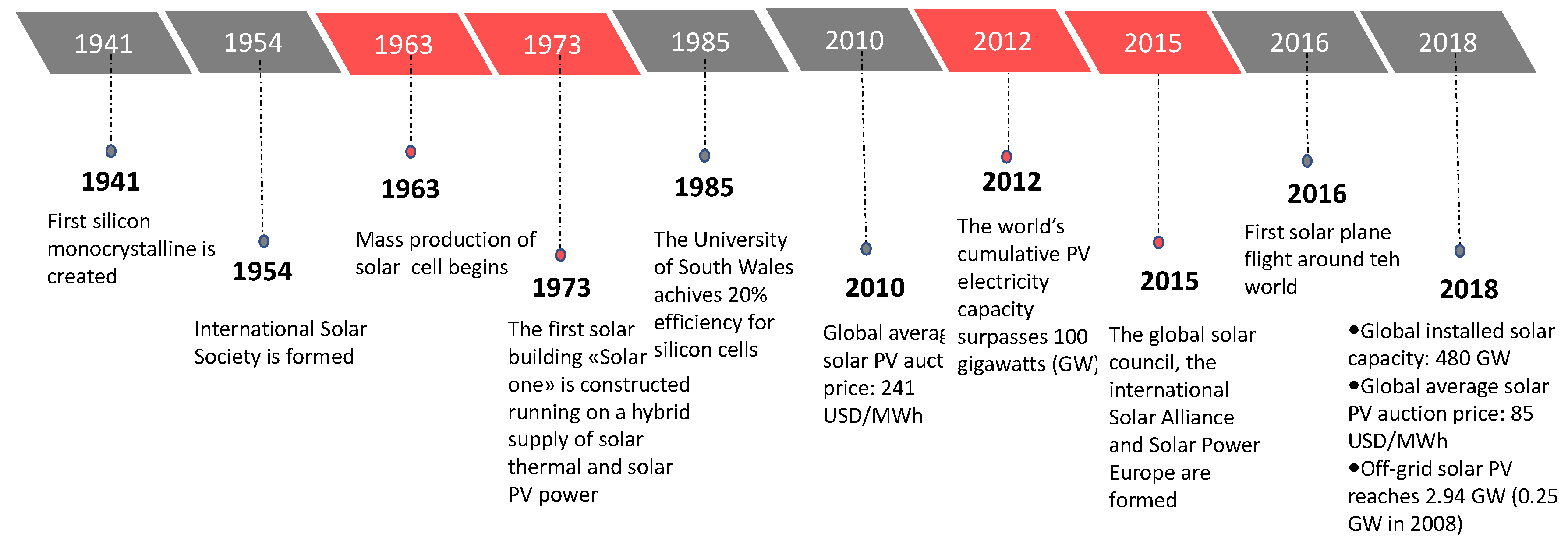
Figure 2.
(A): PV module production per region; (B): global cumulative PV installation [4].
Figure 2.
(A): PV module production per region; (B): global cumulative PV installation [4].
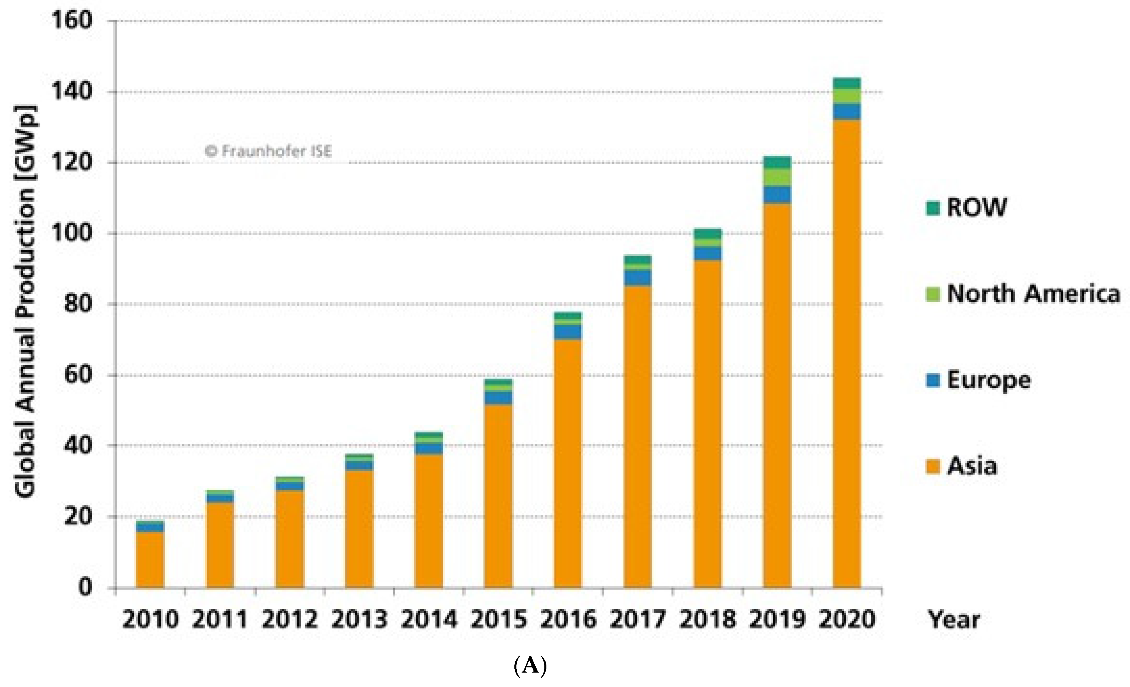
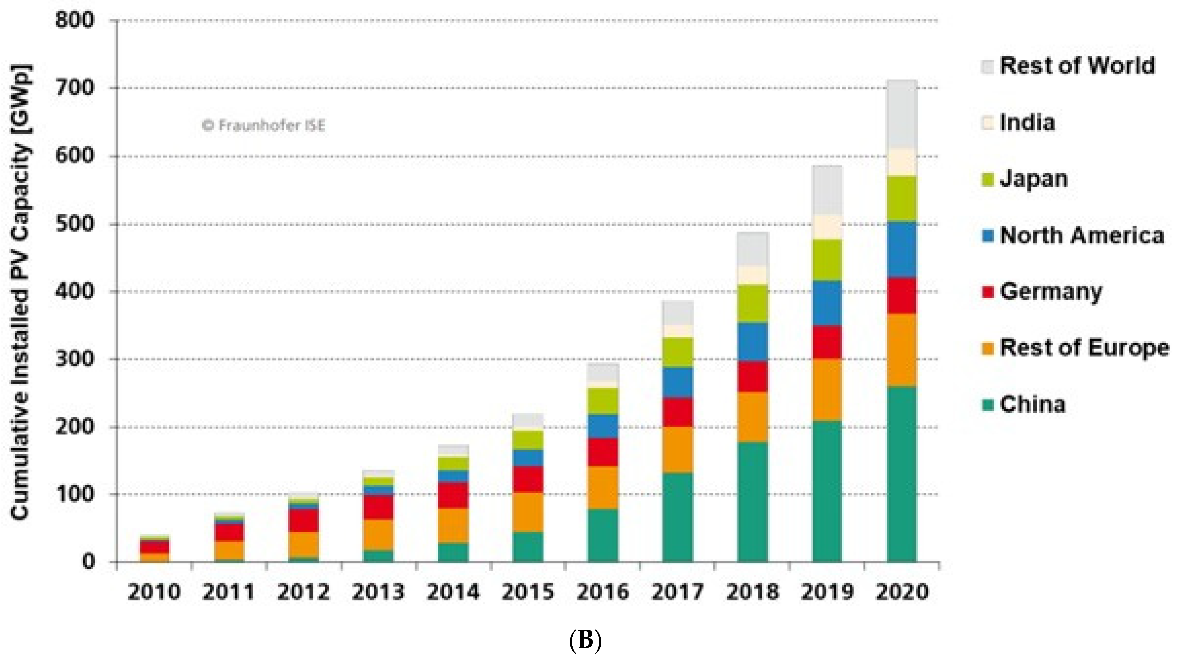
Figure 3.
Solar PV technology status [11].
Figure 3.
Solar PV technology status [11].
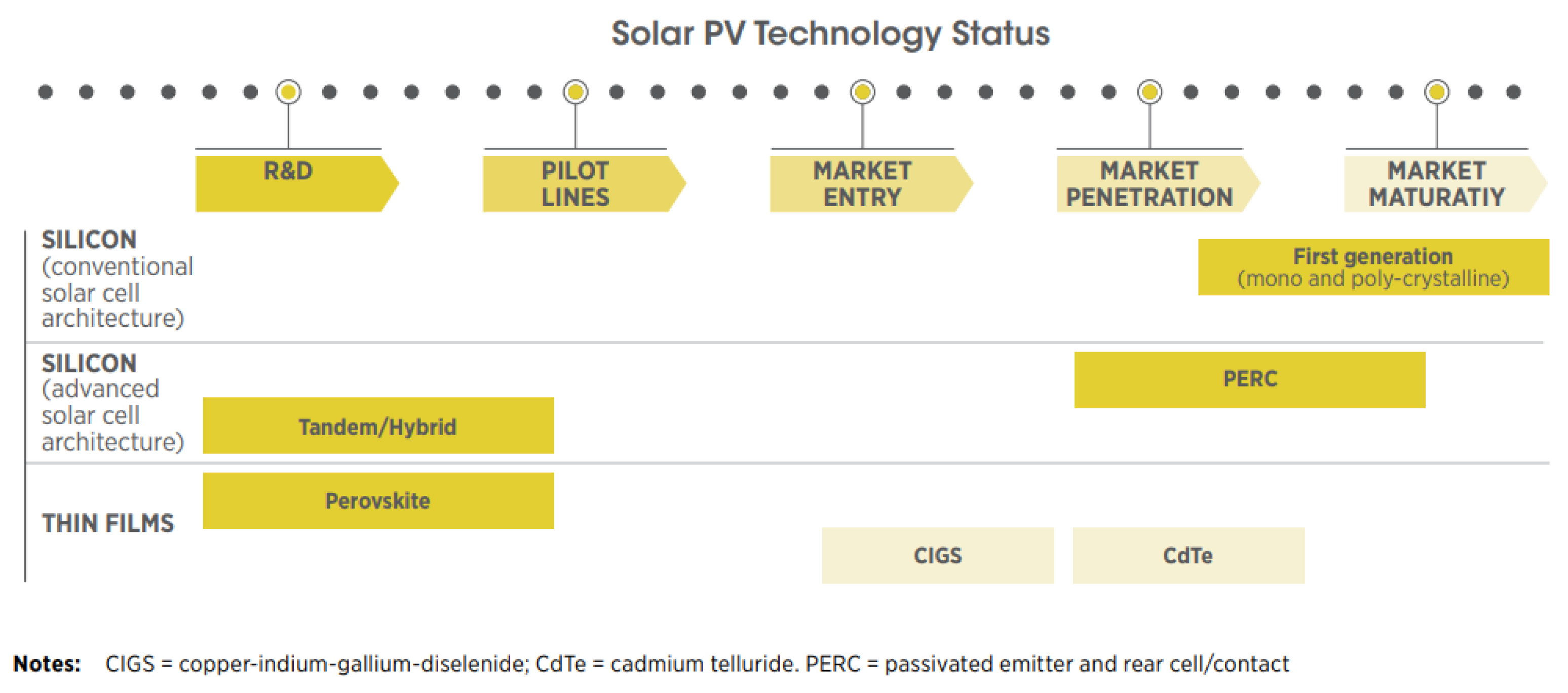
Figure 4.
PV production by technology [4].
Figure 4.
PV production by technology [4].

Figure 5.
Abundance in the Earth’s crust for several elements [17].
Figure 5.
Abundance in the Earth’s crust for several elements [17].
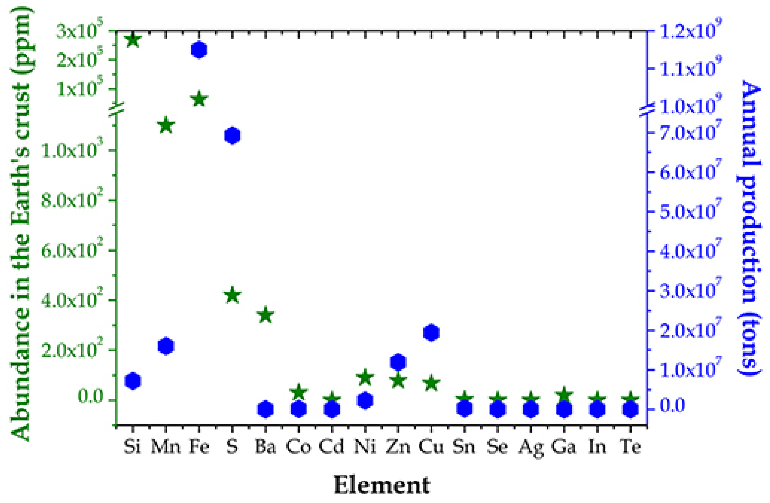
Figure 6.
Annual global production of thin-film PV modules [4].
Figure 6.
Annual global production of thin-film PV modules [4].

Figure 7.
The 90 natural elements that make up everything. How much is there? Is that enough? [24].
Figure 7.
The 90 natural elements that make up everything. How much is there? Is that enough? [24].

Figure 8.
Breakdown of cost components (average of available country data) [4].
Figure 8.
Breakdown of cost components (average of available country data) [4].
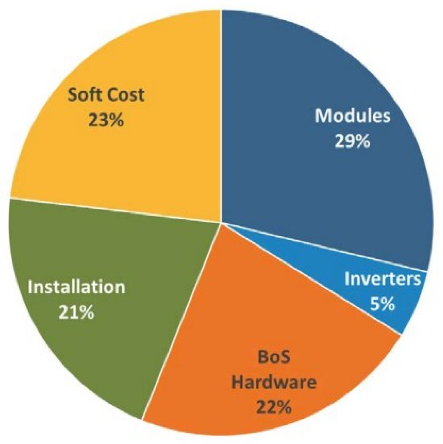
Figure 9.
A typical I–V curve in a solar cell efficiency illustration [51].
Figure 9.
A typical I–V curve in a solar cell efficiency illustration [51].
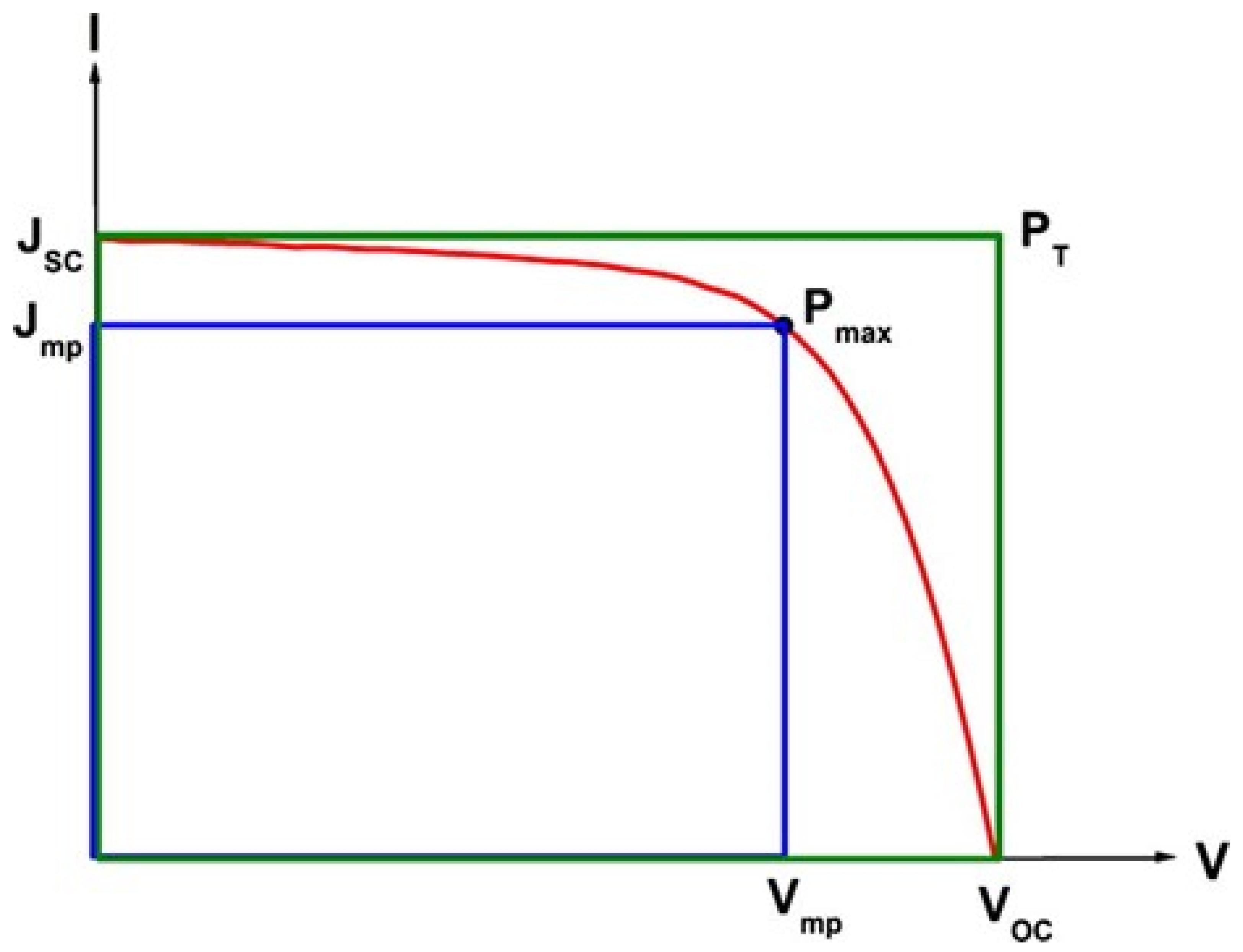
Figure 10.
Record efficiency of solar cells of different materials against their bandgap, in comparison to the SQ limit (top solid line) [50].
Figure 10.
Record efficiency of solar cells of different materials against their bandgap, in comparison to the SQ limit (top solid line) [50].

Figure 11.
Typical architecture of a CZTSSe-based solar cell [64].
Figure 11.
Typical architecture of a CZTSSe-based solar cell [64].

Figure 12.
Efficiency evolution of kesterite and chalcopyrite from the first reported working solar cell [63].
Figure 12.
Efficiency evolution of kesterite and chalcopyrite from the first reported working solar cell [63].

Figure 13.
Schematic diagram of quasi-1-dimensional structures of Sb2S3. (a) Side view and (b) top view of [Sb4S6] ribbons along the c axis. Reproduced from [116] under CCBY 4.0.
Figure 13.
Schematic diagram of quasi-1-dimensional structures of Sb2S3. (a) Side view and (b) top view of [Sb4S6] ribbons along the c axis. Reproduced from [116] under CCBY 4.0.
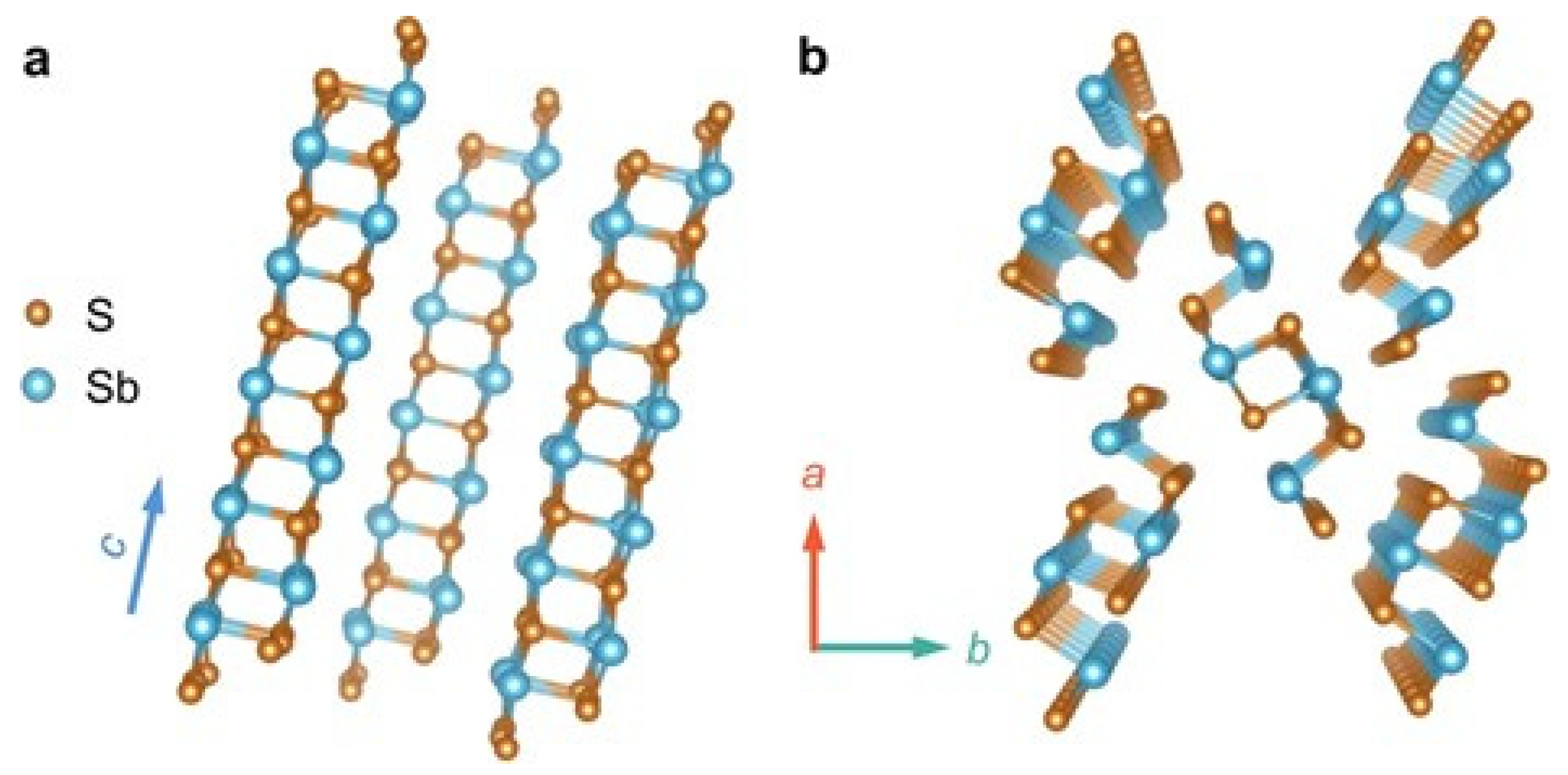
Figure 14.
The effect of asymmetry in the Q1D of Sb2Se3 on Se atomic sites. Reproduced from [106] under CCBY 4.0.
Figure 14.
The effect of asymmetry in the Q1D of Sb2Se3 on Se atomic sites. Reproduced from [106] under CCBY 4.0.
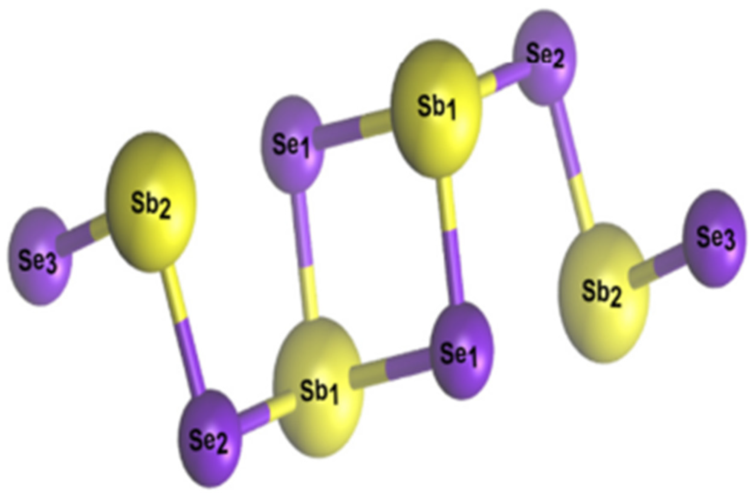
Figure 15.
The effect of grain boundaries in solar cell devices. (a) J–V characteristics of reference solar cells for the CIGSe layers with different AlkF-PDT; (b) open circuit voltage deficit with respect to the respective band gap as a function of the potential change at the GBs for the three studied samples (large colored circles) and for some results taken from the literature; (c) schematic band diagrams (lower panels) and expected CPD as measured by KPFM (upper panels) for a GB with a hole barrier (left), an electron barrier (middle) and an electron barrier with a band offset (right); and (d) schematic of the PDT process. Reproduced from [138], under CCBY 4.0.
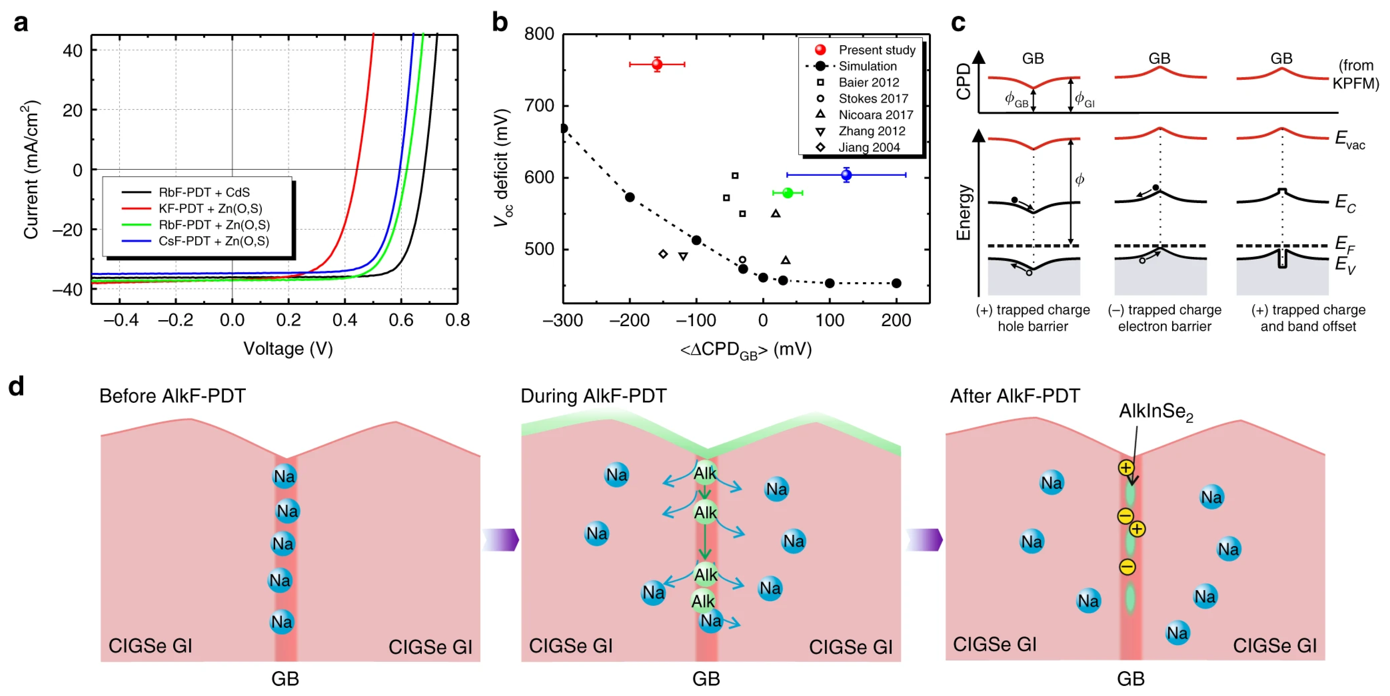
Figure 16.
Climatic zones of India. The black dots indicate the locations surveyed in [151]. Reproduced from [151], under CCBY 4.0.


Table 1.
Major global supplier countries of CRMs [5].
Table 1.
Major global supplier countries of CRMs [5].
| Entry # | Material | Stage | Main Global Supplier | Share (%) | Entry | Material | Stage | Main Global Supplier | Share (%) |
|---|---|---|---|---|---|---|---|---|---|
| 1 | Antimony | E | China | 74 | 23 | Magnesium | P | China | 89 |
| 2 | Baryte | E | China | 38 | 24 | Graphite | E | China | 69 |
| 3 | Bauxite | E | Australia | 28 | 25 | Natural rubber | E | Thailand | 33 |
| 4 | Beryllium | E | USA | 88 | 26 | Neodymium | E | China | 86 |
| 5 | Bismuth | P | China | 80 | 27 | Niobium | P | Brazil | 92 |
| 6 | Borate | E | Turkey | 42 | 28 | Palladium | P | Russia | 40 |
| 7 | Cerium | E | China | 86 | 29 | Phosphate rock | E | China | 48 |
| 8 | Cobalt | E | Congo, DR | 59 | 30 | Phosphorous | P | China | 74 |
| 9 | Coking coal | E | China | 55 | 31 | Platinum | P | South Africa | 71 |
| 10 | Dysprosium | E | China | 86 | 32 | Praseodymium | E | China | 86 |
| 11 | Erbium | E | China | 86 | 33 | Rhodium | P | South Africa | 80 |
| 12 | Europium | E | China | 86 | 34 | Ruthenium | P | South Africa | 93 |
| 13 | Fluorspar | E | China | 65 | 35 | Samarium | E | China | 86 |
| 14 | Gadolinium | E | China | 86 | 36 | Scandium | P | China | 66 |
| 15 | Gallium | P | China | 80 | 37 | Silicon | P | China | 66 |
| 16 | Germanium | P | China | 80 | 38 | Tantalum | E | Congo, DR | 33 |
| 17 | Hafnium | P | France | 49 | 39 | Terbium | E | China | 86 |
| 18 | Ho, Tm, Lu, Yb | E | China | 86 | 40 | Titanium | P | China | 45 |
| 19 | Indium | P | China | 48 | 41 | Tungsten | P | China | 69 |
| 20 | Iridium | P | South Africa | 92 | 42 | Vanadium | E | China | 39 |
| 21 | Lanthanum | E | China | 86 | 43 | Yttrium | E | China | 86 |
| 22 | Lithium | P | Chile | 44 | 44 | Strontium | E | Spain | 31 |
Legend: E = extraction stage; P = processing stage.
Table 2.
Comparison of first- and second-generation PV solar cells in terms of sustainability indicators [13].
Table 2.
Comparison of first- and second-generation PV solar cells in terms of sustainability indicators [13].
| Solar Cell | LCA (MJ/m2) | EPBT (Year) | GHC (g CO2-eq/kW h) |
|---|---|---|---|
| mono-Si | 2860–5253 | 1.7–2.7 | 29–45 |
| Multi-Si | 2699–5150 | 1.5–2.6 | 23–44 |
| Thin film | |||
| a-Si | 710–1990 | 1.8–3.5 | 18–50 |
| CdTe | 790–1803 | 0.75–2.1 | 14–35 |
| CIS | 1069–1684 | 1.45–2.2 | 10.5–46 |
Table 3.
Some critical elements and global (%) recovery as hitchhikers [20].
Table 3.
Some critical elements and global (%) recovery as hitchhikers [20].
| Element | Symbol | Production as Hitchhiker % | Attractor Metal |
|---|---|---|---|
| Rare Earths | REE | 47 | Fe |
| Antimony | Sb | No data | Au, Cu, Pb |
| Molybdenum | Mo | 100 | Cu |
| Germanium | Ge | 100 | Zn |
| Gallium | Ga | 100 | Al |
| Indium | In | 100 | Zn |
| Platinum | Pt | 100 | Cu, Ni |
| Palladium | Pd | 100 | Cu, Ni |
| Rhodium | Rh | 100 | Pt/Pd |
| Ruthenium | Ru | 100 | Pt/Pd |
| Cobalt | Co | 85 | Ni 50% Ru 35% |
| Selenium | Se | 100 | Cu |
| Vanadium | V | 74 | Fe 59%, Al, U |
| Tellurium | Te | 100 | Cu |
Table 4.
Efficiency comparison of some PV technologies.
| Entry | Material | Cell Efficiency (%) Year | Module Efficiency (%) Year | ||
|---|---|---|---|---|---|
| 2016 | 2021 | 2016 | 2021 | ||
| 1 | Mono-crystalline Si | 25.3 [37] | 26.7 [4] | 22.4 [37] | 24.4 [4] |
| 2 | Multi-crystalline Si | 21.9 [37] | 24.4 [4] | 18.5 [37] | 20.4 [4] |
| Thin film | |||||
| 3 | a-Si | 12.7 [37] (2015) | - | 12 [56] | - |
| 4 | CIGS | 22.6 [37] | 23.6 [37] | 17.5 [37] | 19.2 [4] |
| 5 | CdTe | 22.3 [37] | - | 18.6 [37] | 19.0 [4] |
| 6 | CZTS | 9.5 [37] | 13.0 [37] | n.a. | n.a. |
| 7 | SbSSe | 5.79 [57] | 10.1 [41] | n.a. | n.a. |
Table 5.
Main deposition methods of the active layer in PV thin films.
| Method | General Features |
|---|---|
| Vacuum techniques | Controlling the film composition and the corresponding phase profile. A considerable amount of energy is required to deposit material from the target sources, and the relatively slow throughput and low utilization of materials are not beneficial for large-scale production [83]. |
| Sputtering | [84,85] |
| Atomic Layer Deposition (ALD) | [86,87] |
| Thermal evaporation | [88,89] |
| Vapor Transport deposition (VTD) | [90,91] |
| High Vapor Transport Deposition (HVTD) | [61] |
| Vacuum electrodeposition | [92] |
| Non-vacuum techniques | Reduced capital equipment costs, lower temperature process, higher suitability for large-area and flexible substrates, higher throughput. |
| Spray pyrolysis | [93,94] |
| Chemical Bath Deposition (CBD) | [95,96,97] |
| Sol-gel | [98,99,100] |
| Hydrothermal methods | [101] |
| Spin coating | [102] |
| Dip coating | [102] |
| Spray coating | [102] |
| Electrodeposition | [103,104] |
Table 6.
Performance parameters and fabrication methods of recent Sb2(S,Se)3 solar cells.
| Entry | Absorber Material Thin-Layer | HTL, Counter Electrode | Electron Transport Material (ETM) | Fabrication Method | Power Conversion Efficiency (η, %) | VOC (V) | Remarks | Year | Ref. |
|---|---|---|---|---|---|---|---|---|---|
| 1 | Sb2 (S,Se)3 | Spiro-OMeTAD *, Au | FTO **/TiO2 | Solution (one-step spin-coating deposition) | 5.8 | 0.52 | -DMF, a weak basic solvent, enables simultaneous dissolution of Se and Sb2O3 with carbon disulfide (CS2) and n-butylamine (nBA) in the solution. -Pure crystal phase is obtained. -Abundant pin holes, responsible for low efficiency. | 2018 | [126] |
| 2 | Sb2 (S,Se)3 | C, Ag | FTO/CdS | Thermal evaporation | 5.74 | 0.48 | Composition of the films may be varied along its thickness in the thermal evaporation. Graphite electrode: the basic consideration here was the ease of preparing an electrode with a work function of near 5 eV for the p-side, which was not chemically reactive with antimony chalcogenide. | 2019 | [127] |
| 3 | Sb2(S,Se)3 | Spiro-OMeTAD, Au | FTO/TiO2 | Solution (one-step spin-coating deposition) | 4.49 | 0.53 | The solution is composed of 1.0 mmol of Sb2O3, 1.0 mmol of Se, and 0.1 mmol of CsOH· xH2O, mixed solvent of 2.0 mL of DMF and 1.5 mL of carbon disulfide, 2.0 mL of n-butylamine was added. | 2019 | [128] |
| 4 | Sb2(S,Se)3 | Spiro-OMeTAD, Au | FTO/TiO2/CdS | Solution (one-step spin-coating deposition) | 4.74 | 0.61 | The solution is the same as entry 3. The efficiency increase is due to the difference: FTO/TiO2/CdS instead of FTO/TiO2. | 2019 | [128] |
| 5 | Sb2 (S,Se)3 | Spiro-OMeTAD, Au | FTO/TiO2/In:CdS | Solution (one-step spin-coating deposition) | 6.29 | 0.59 | The solution is the same as entry 3. The efficiency increase is due to the difference: FTO/TiO2/In:CdS instead of FTO/TiO2. | 2019 | [128] |
| 6 | Sb2 (S,Se)3 | Spiro-OMeTAD, Au | FTO/TiO2/In:CdS | Solution (one-step spin-coating deposition) | 6.63 | 0.59 | The solution is the same as entry 3. The efficiency increase is due to the difference: FTO/TiO2/In:CdS instead of FTO/TiO2. | 2019 | [128] |
| 7 | Sb2(S,Se)3 | Spiro-OMeTAD/Au | FTO/CdS | Two-step synthesis: -In situ hydrothermal growth; -Post selenization. | 6.14 | 0.732 | This study unveils the great potential of the hydrothermal method in the fabrication of high-performance Sb2(S,Se)3 thin film solar cells. | 2019 | [129] |
| 8 | Sb2 (S,Se)3 | CsPbBr3 QDs, Au | FTO/CdS | Two-step synthesis: -In situ hydrothermal growth; -Post selenization. | 7.82 | 0.620 | This study shows another application of perovskite materials and a practical strategy towards the efficiency improvement of Sb2(S,Se)3 solar cells. | 2020 | [130] |
| 9 | Sb2 (S,Se)3 | Spiro-OMeTAD/Au | FTO/CdS | Two-step synthesis: -In situ hydrothermal growth; -Annealing under N2. | 10.1 | 0.630 | Antimony potassium tartrate (APT), sodium thiosulfate (STS), and selenurea (SU) were used as sources of antimony, sulfur, and selenium, respectively, in the hydrothermal system. Through the optimization of the hydrothermal deposition parameters and subsequent annealing, high quality Sb2(S,Se)3 films with an optimal morphology grain size and a reduced number of defects can be obtained. | 2020 | [115] |
| 10 | Sb2 (S,Se)3 | Spiro-OMeTAD/Au | FTO/CdS | Two-step synthesis: -In situ hydrothermal growth; -Annealing under N2. | 10.5 | 0.664 | Ethylen diaminetetraacetic acid (EDTA) was added to the hydrothermal mixture of APT, STS, and SU (the same used in [104], entry 9), resulting in an improvement in film quality and electrical properties. | 2020 | [131] |
| 11 | Sb2 (S,Se)3 | Spiro-OMeTAD/Au | FTO/Zn(O,S)/CdS | Three step synthesis: - In situ hydrothermal growth; -Solution post treatment (SPT) using alkali metal fluorides as additives (NaF, KF, RbF, and CsF); -Annealing. | 10.7 | 0.673 | An alkali fluoride post treatment is capable of vertically manipulating the Se/S distribution and forming additional favorable Se/S gradient distribution. | 2022 | [125] |
* 2, 2′, 7, 7′-tetrakis (N, N-dipmethoxyphenylamine)-9, 9-spirobifluorene (Spiro-OMeTAD), ** fluorine-doped tin oxide (FTO).
Disclaimer/Publisher’s Note: The statements, opinions and data contained in all publications are solely those of the individual author(s) and contributor(s) and not of MDPI and/or the editor(s). MDPI and/or the editor(s) disclaim responsibility for any injury to people or property resulting from any ideas, methods, instructions or products referred to in the content. |
© 2023 by the author. Licensee MDPI, Basel, Switzerland. This article is an open access article distributed under the terms and conditions of the Creative Commons Attribution (CC BY) license (https://creativecommons.org/licenses/by/4.0/).
Share and Cite
MDPI and ACS Style
Buonomenna, M.G. Inorganic Thin-Film Solar Cells: Challenges at the Terawatt-Scale. Symmetry 2023, 15, 1718. https://doi.org/10.3390/sym15091718
AMA Style
Buonomenna MG. Inorganic Thin-Film Solar Cells: Challenges at the Terawatt-Scale. Symmetry. 2023; 15(9):1718. https://doi.org/10.3390/sym15091718
Chicago/Turabian StyleBuonomenna, Maria Giovanna. 2023. "Inorganic Thin-Film Solar Cells: Challenges at the Terawatt-Scale" Symmetry 15, no. 9: 1718. https://doi.org/10.3390/sym15091718
Note that from the first issue of 2016, this journal uses article numbers instead of page numbers. See further details here.