Review

The Atomistic Structure of Metal/Ceramic Interfaces Is the Key Issue for Developing Better Properties

by
Wilfried Wunderlich
Material Science Department, Faculty of Engineering, Tokai University, 259-1292 Hiratsuka, Japan
Metals 2014, 4(3), 410-427; https://doi.org/10.3390/met4030410
Submission received: 3 June 2014 / Revised: 9 August 2014 / Accepted: 11 August 2014 / Published: 20 August 2014
(This article belongs to the Special Issue Advances in Cermets)

Abstract

:
Metal-metal-, ceramic-metal-composites (MMC, CMC) and related functional materials are steadily gaining interest for practical applications. This invited overview paper is divided into three parts. First, the importance of interfaces in material science is emphasized, then basics of computer modeling of interfaces on atomic scale is outlined, followed by the description of some interface examples and their applications. Atomistic modeling requires the specific determination of the orientation relationship between both crystal lattices facing the heterogeneous interface, the interface plane, and translation vectors of two facing crystals. Examples of the atomistic structure are described in this paper for interfaces, such as MgO/Ag, MgO/TiN, Al2O3/Fe, and others. The trend in this research is gradually, but steadily shifting from structural towards functional materials, because atomic binding at interfaces offers a broad spectrum of new properties to be utilized for applications.

Graphical Abstract

1. Introduction

While atoms are the smallest units for solid-state physicists, interfaces are the smallest building units for material scientists. Heterogeneous interfaces between two different types of materials change the chemical bonding and new properties are formed. This review focuses on inorganic materials, such as metals, semiconductors, ceramics and the interfaces in between, but just as a vision for future development of interfaces, the invention of a new adhesive material “super-gecko” is reviewed. Bio-inspired research found first the reason for [1], then the mechanism of setae [2], and finally it could be mimicked as synthetic composites [3] with further improvement [4]. Reversible interfacial bonds are considered to be realized by van-der-Waals bonds. Metal-ceramic-interfaces are formed by the other three types of atomic bonds, hence strongly and irreversible bonded, and can only be release under special hydrogen treatment [5]. Metal-ceramic-interfaces have been known for long-time as enamel in pottery [6], and became popular as a research topic when atomistic-scale analysis of metal-ceramic-interfaces became possible by high-resolution transmission electron microscopy (HRTEM) around 1985 [7], and soon afterwards by ab initio simulations [8,9,10] and finite element modeling (FEM) [11]. Since then, metal ceramic interfaces with advanced mechanical properties play an important role as thermal barrier coatings (TBC) on high temperature materials, for example yttria stabilized zirconia (YSZ) coated on Ni3Al turbine blades. Many reviews have been published [11,12,13,14,15,16,17,18,19,20,21].
Interfaces came again into the focus of public society, when in 2007, both the Nobel prizes for chemistry and for physics were awarded for interface research: thin films on surfaces enhance chemical reactions [22] and opened the door for research on environmental protection [23,24], and thin interface layers show giant magneto resistance (GMR) [25,26]. This development shows the trend that functional materials demand more and more interface research, because possibilities for applications increase. Representative examples of present research on inorganic interfaces are thermal-barrier coatings (TBC) [27,28,29,30], hard TiN-coating [31,32,33,34,35], superconductors [36], and as functional components in microelectronics [37,38,39,40,41,42], transparent conducting oxides (TCO) [43,44,45,46], photovoltaic materials [47], thermo-electrics [48,49,50,51,52], ferroelectrics [53], magnetic materials or spintronics [54,55].
This paper focuses mainly on metal- ceramic interfaces, but other inorganic crystalline interfaces are partly included because their principles are similar, while organic materials are excluded. First, we describe the manufacturing methods and the motivation as to why interfaces gain interest, followed by a description of how to build an atomic model of interfaces. The main part of this paper, Section 4, describes experiments and modeling of interfaces on an atomic scale and their influence on properties. The last sub-section explains the electron transport and the device geometry.

2. Increasing Importance of Inorganic Interfaces

Research on metal-ceramic interfaces and their composites is steadily growing as they offer possibility for new electronic devices or mechanical parts with better properties. In a broader context, Figure 1 summarizes the characteristics of competitive joining and deposition techniques for manufacturing inorganic thin films or interfaces in composite materials in general. Mechanical deposition is cheapest and can be performed by spraying, painting, spin- or dip-coating. Physical deposition can be categorized into mechanical bonding, condensation or sputtering. Bonding means usually applying pressure and temperature, in the case of diffusion bonding, while surface activated bonding (SAB) is used in microelectronics after the discovery that cleaned and atomically flat polished surfaces can be bonded with relatively low pressure and low temperature [37,38]. In the case of soldering, brazing and welding, often lubricants or inserts are added and the temperatures are higher. Selective laser sintering (SLS) is one of the recently developed processing methods for 3D printing, which is one of the methods for additive manufacturing. This so-called additive manufacturing (AM), a relatively new processing technique, piles up successively layer-by-layer of material, making rapid prototyping of devices or interface research reasonable cheap.
Figure 1. Categorization of several deposition techniques for thin film deposition or interface.
Metals 04 00410 g001
The next column in Figure 1 shows condensation methods. Most of these methods require a vacuum, such as physical vapor deposition (PVD), with the exception of liquid phase epitaxy (LPE). The next column shows the sputtering techniques, such as molecular beam epitaxy (MBE), radio frequency (RF) magnetron or pulsed laser deposition (PLD). These rather expensive methods with their slow growth rates usually guarantee atomically perfect epitaxial growth with strong bonds. Finally, the traditional methods of metal or enamel plating are shown in the last column. Chemical bonding methods are usually cheaper than others are, but require relative expensive precursors for sol-gel, Langmuir techniques, atomic layer deposition (ALD), chemical solution deposition (CSD). Magneto-optical or plasma enhanced chemical vapor deposition (MOCVD, PECVD) require gas flow. Important process parameters are substrate temperature [42], vapor pressure and power. With each new decade, new techniques arise; this list is probably incomplete and needs to be updated soon.
Thin films coating for improving mechanical properties started from mechanically surface hardened steels, then proceeded to coated drills and TBC for turbines. Nowadays coatings and especially metal-ceramic interfaces have become essential for many other applications, such as semiconductor devices, transistors, diodes, integrated chips, optical thin films, sensors for gas, electric or magnetic fields, actuators, manipulators, magnetostriction devices, and devices for heterogeneous catalysis. These applications for microelectronics, photo catalysis, photovoltaic, as thermal barriers, or for corrosion protection, are a few but representative examples.
Figure 2 shows one of the most urgent fields of research in our age, finding new technologies for energy supply. While solar cells were initially invented on poly- and single crystalline bulk-Si, they soon changed to thin-film technology, because devices can be built cheaper without reducing performance. Such a learning curve as in Figure 2 can be drawn for any technology and describes the production cost as dependence on the installed number of equipment; data are taken from [50]. Thin-film photovoltaic became much cheaper than those based on crystalline materials, so the opinion became popular that the same trend should occur for thermoelectrics and as a result, many TE thin-film research projects were proposed. Such self-promoting trends are the driving force for new technologies, such as 3D-printing and additive manufacturing. This field of research will gain further popularity in the near future.
Figure 2. The learning curve compares the production costs for energy from renewable sources as a function of the installed power. PV-cry, photovoltaic crystalline; PV-ThF, photovoltaic thin film.
Metals 04 00410 g002
Planar thin film geometry is only one of many other possible interface geometries. Figure 3a shows on the x-axis a typical geometrical parameter, such as inverse aspect ratio rx/ry or inverse bending radius 1/rx. A simple planar interface has 1/rx << 1, round particles have rx/ry = 1. The geometry becomes more complex [56,57], when the aspect ratio rx/ry > 1 forming rods, or tubes, or even more sophisticated grain boundary precipitates. The parameter on the y-axis is the constraint, which means whether an interface is in its relaxed state (low constraint) or far from equilibrium (highly disturbed). The more sophisticated a processing technology becomes, the more parameters are possible. Thus, these artificially produced interfaces contain highly non-equilibrium states or phases, requiring post-annealing for stabilization. Examples for interfaces far from equilibrium are those in spark-plasma sintered (SPS) composites [58], spraying of TBC-surfaces with high mechanical pressure, or plasma- coated composites incorporating a large amount of defects. On the other hand, some metastable phases have a rather long-term stability [59], if kept below moderate temperatures.
As the complexity [56,57] increases from bottom left to upper right in Figure 3a, we proceed from relaxed natural planar interfaces to constrained or bended interfaces with more possibilities for engineering their properties. There has been a debate whether inserted layers at interfaces are thermodynamically stable or better considered a separate phase called “complexion” [56,57,58]. When the diameter of particles decreases below 10 nm, so-called nano-size effects occurs, see Figure 3b,c. The first one, as shown in Figure 3b, is the well-known ratio of atoms sitting at well-defined crystalline positions versus those sitting at the grain boundaries. The later atoms experience reduced coordination numbers and disturbed positions. The ratio of such amorphous-like bonded atoms increases from less than 1% in polycrystalline material to more than 50% in nano-cyrstalline material, when the grain diameter drops below 10 nm. This effect was found on nano-crystalline materials and confirmed by HRTEM-studies [60].
Figure 3. (a) Increasing complexity of interfaces in a schematic diagram of geometrical features and constraints; (b,c) Nano-size effects of properties due to interfaces: (b) volume fraction of disturbed atoms; (c) curvature of interfaces.
Metals 04 00410 g003
The second nano-size effect (Figure 3c) mainly changes the properties of functional materials. While a planar interface has an infinite bending radius, the amount of bending as expressed by the inverse radius 1/rx increases in one axis when we bend it to a rod. If we bent in two axes, we get a disc or tube. If we bent the interface in three axes, we get round-shaped particles. Molecular Dynamics (MD) calculations [61] showed that concave surfaces like spheres increase their interface energy, hence making them more reactive, when the radius decreases below a critical one of about rc < 10 nm. On the other hand, the surface energy of nano-pores decreases below rc. The smaller they become, the harder it is to extinguish them, which means they are self-stabilized. This splitting in physical properties below a critical radius can be used for engineering purposes, as indicated by calculations of the author [61,62] and confirmed experimentally by others [63].
Figure 4. Ratio of coating layer volume versus core volume as a function of nano-particle radius and coating layer thickness.
Metals 04 00410 g004
One popular example for functional nano-materials are isolated Fe-particles with their ability of fast spin response to applied magnetic fields. When their radius drops below 10 nm, they show enhanced magnetic properties, which demonstrate the highest coercitivity [64]. A small diameter is best for a fast response. However, for stabilizing metallic nano-sized particles, their surfaces need to be passivated by oxide layers in order to prevent agglomeration [64,65]. Such core-shell nano-powders became popular after reasonable coating techniques were available. Figure 4 shows the volume fraction of Vcoating/Vcore as a function of particle radius and coating thickness, showing that particles with small radius and thin coating layer thickness are desired.

3. Atomistic Simulations

Heterogeneous interfaces are interfaces between materials with different chemical composition and/or crystal lattice or orientation. When the interface is naturally formed, in most cases a defined orientation relationship between both lattices occurs, which has its origin in the fact that long-range coulomb forces want to keep atom positions of both lattices in concordance with each other even across the interface. It has been proven that the interface strength is higher when the so called coincidence site lattice (CSL) has higher density. The interfaces are distinguished in coherent, semi-coherent or incoherent interfaces, whether the lattice spacing structure of both lattices matches perfectly, matches partly, or not at all. A rule of thumb states that perfect matching occurs up to a lattice mismatch of tensile or compressive stress up to ±5% or ±10%. This limit of elastic distortion on nano-scale differs for each material combination. The elastic deformation accommodates the difference in lattice spacing and causes changes in the materials properties. In the case of thin films, this strain can be used for engineering purpose and an example is the band-gap of TiO2 described in Chapter 4.4. In the following paragraphs, we will focus on coherent interfaces, and examples are shown in the next section.
When the mismatch between the two facing lattices becomes larger, elastic strain is not sustainable anymore and misfit dislocations are formed. Finally, when the strain exceeds more than ±20%, the role of the interface almost disappears. Such random interfaces are by far the most common ones, but we will exclude them from now on, because they cannot easily be controlled and their complexity prevents engineering. Some interfaces are likely to form amorphous regions at the interface plane, some show segregation, or even grain boundary precipitates, or enhanced diffusivity with large change in chemical composition.
Coherent interfaces can be treated by bi-crystallography. Similar to grain boundaries, the same rules as in crystallography can be applied to the two heterogeneous lattices facing an interface. The only difference is that additionally the atom can change its type, while the crystallographic site is maintained across the interface. Interfaces between metals and their oxides tend to keep the anion site position across the interface [7,8,13,15,16,17], even though the larger oxide lattice changes the symmetry. FeO and ZrO2 possess fcc anion sub-lattices, while their metal phase is different. On the other hand, at interfaces between different oxide materials, the cation sub-lattices are maintained, because of the larger volume of oxygen ions.
The two lattices have a certain orientation relationship, which can be expressed by a rotation axis and angle. In practice, however, it became much more popular to express the two facing planes and directions. For example, in the case of thin films, the substrate has a certain surface and by X-ray diffraction (XRD) or TEM, it soon can be analyzed whether the thin film fits to that. These experimental data are necessary for modeling, as many different combinations of coherent interfaces could be possible.
The procedure for modeling interfaces on atomic scale is sketched in Figure 5. First, we need the crystallographic information of both lattices, namely their lattice parameters, symmetry group and atomic positions inside the unit. Then we rotate both unit cells according to the orientation relationship. This makes it necessary to transform crystals with six-fold symmetry to a rectangular cell, because it is easier for us to think in three dimensions. In other words, it has become common to transform each of the two facing crystals of an interface to a coordinate system with x- and y-axes parallel to the interface plane, and z-axis perpendicular to it. The example in Figure 5a shows in red a metal lattice unit, expanded several times on x-, y-, z-axes, in order to fit to the lattice constants of the ceramic lattice. The matching in z-direction is also important, because most MD and ab initio software programs use periodic boundary conditions. When putting both of the two lattices together, we have still three parameters of freedom that are the relative translation vectors within the interface plane or perpendicular to it. Experimentally they cannot be determined by XRD, only by HRTEM. If they are not known, an initial guess is usual obvious, but checks by Molecular Dynamics (MD) or ab initio MD (aiMD) runs are necessary. There is one last important item to be checked before a MD simulation is started, that is the individual relaxations of atoms close to the interface plane. If two atoms have a bonding distance too close to each other in the input configuration, one of them needs to be removed.
Figure 5. Modeling metal/ceramic interfaces with a certain orientation relationship requires inclusion of (a) misfit dislocations and/or; (b) difference in thermal expansion.
Metals 04 00410 g005
With relaxed structures, ab initio simulations can finally be started for the calculations of properties. The goal of this simulation is to find the stable structure of an interface, which is the base for further properties calculations. Similar as in single crystals, the crystallography of interfaces, so-called bi-crystallography has become an own field of science. It is the goal to find and characterize the structural units, which are formed at the interfaces and which are usual different from bulk units due to their difference in bonding partners. When the MD simulation has reached a low energy state, how can we be sure that this an interface model close to reality? Usual this question is answered by its success, namely when we reach the same final structure and state from different input structures. With this relaxed structure further simulation of properties can be performed. As such, interface modeling requires many steps, usual only interfaces with simple or obvious structures are calculated, as shown in the next section.
The experience with MD-simulations showed that as in any simulation too, the MD method is an approximation and strongly relies on interaction potentials. Sometimes the lattice constants can differ slightly from the real ones with an error usually less than 10%. Due to the small deviation in the lattice constant, the result of calculating the distance of misfit dislocation has changed, and one should be aware of the limitations of such simulations. The main MD result of this interface could confirm the formation of stacking fault at the interface [66]. After the structural model of an interface has been established, we can now proceed to properties as shown in the next section.

4. Experimental and Calculation Results

The following examples show main principles of interfaces in structural and functional materials. We start from simple interfaces, then we explain the strained thin films with its large engineering impact, and close with confined electron transport on interfaces.

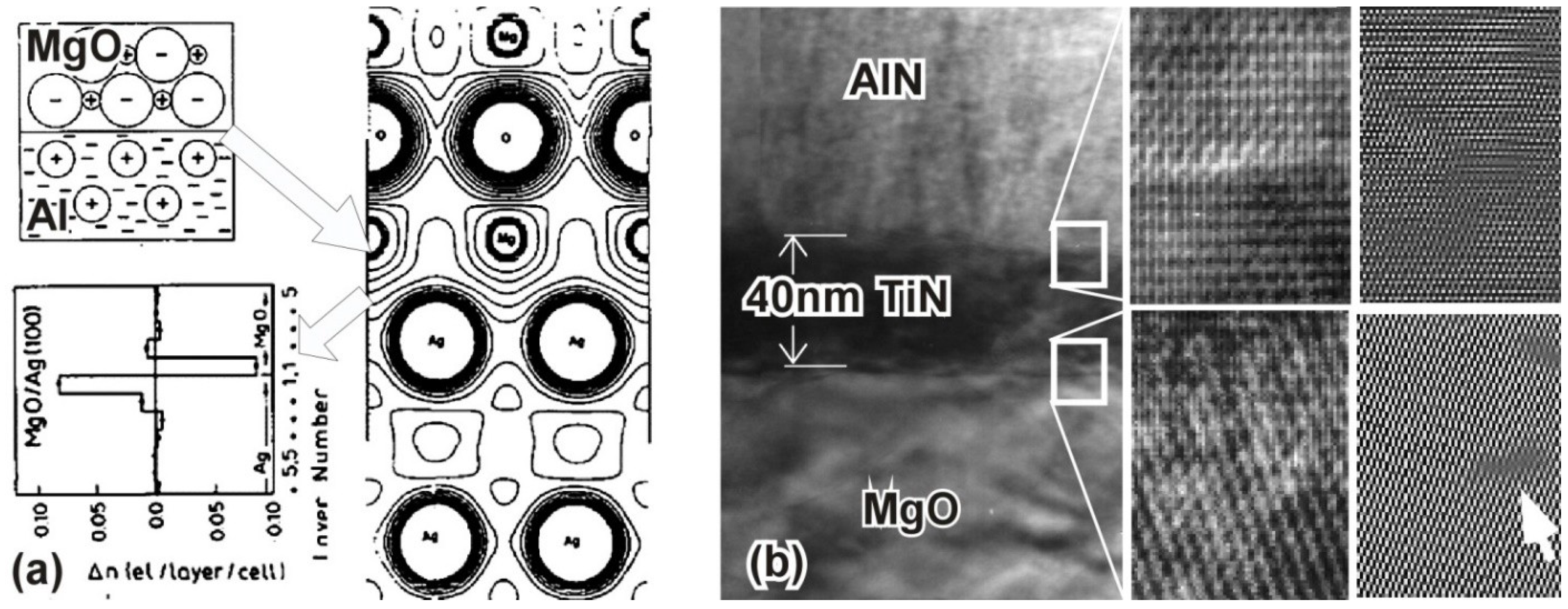
4.1. MgO/Ag Interface: Change of Electron Density

When studies of metal-ceramic interfaces became popular, metallic thin films were sputtered onto MgO substrates, because MgO single crystal can be grown easily and by cleavage (100) surfaces obtained [15,16,17]. Furthermore, the lattice constants of noble metals like Ag, Cu, Au are similar to MgO (100) surface forming a coherent interface with cube-to-cube orientation. Figure 6a shows the first meaningful ab initio simulations based on density-functional theory (DFT) of a metal-ceramic interface (Ag/MgO) [8], soon confirmed by others [9,67].
Figure 6. (a) First meaningful ab initio calculation of an metal-ceramic interface [8], model of the Ag/MgO interface, charge density at the interface, which differs significantly from each layer of the two bulk crystals; (b) TEM and HRTEM micrographs of the MgO/TiN/AlN interface including high-resolution images and filtered image showing only one misfit dislocation as marked by the arrow. (Figures reprinted with permission from publishers [8,18]).
Metals 04 00410 g006
The astonishing result was that the contour plots of the charge density at Ag-Mg-bond at the interface are neither covalent like in MgO, nor metallic. As shown in Figure 6a on the left, the electron charge at Ag is enhanced, while on the MgO it is decreased forming bonds that are unique for this interface.

4.2. MgO/TiN/GaN Interface—Avoiding Misfit Dislocations

The next example of a ceramic-ceramic interface (Figure 6b) illustrates the suppression of misfit dislocations in an AlN thin films sputtered onto a MgO substrate, for details see [68]. As the mismatch between the MgO and AlN lattice constants would be too large, an intermediate buffer-layer of TiN, 40 nm in thickness was sputtered first. The buffer layer successfully avoids the misfit dislocation as confirmed by the image filtered micrograph. As marked by an arrow on the right side of Figure 6b, only a single dislocation at the MgO/TiN interface is detected. As TiN has the same crystal structure as MgO (NaCl structure), the interface between both is hard to detect in the TEM micrographs. Only the absorption contrast due to heavier Ti atom changes the appearance. The orientation between the hexagonal AlN lattice with wurtzite crystal structure and the cubic TiN has the common relationship (0001) AlN//(111) TiN. In addition, this interface shows perfect coherence on atomic scale.
In contrast, misfit dislocations with screw character can contribute to ductility of intermetallic phases as observed at TiAl/Ti3Al interfaces [69,70]. The relationship (0001)hex//(111)cub between hexagonal and cubic lattices is very common at metallic or intermetallic interfaces, because lattice planes with large atomic density face each other. When the cubic lattice becomes slightly tetragonal distorted, a large variety of sets of misfit dislocations can occur, either in one, two or all three directions depending on the c/a ratio of the tetragonal distortion. Such tetragonal distortion can be adjusted in a wide range by additions of Cr and hence could improve the ductility of this alloy.

4.3. TiO2/SrTiO3 and TiO2/Al2O3 Interfaces: Strain Engineering of Epitaxial Grown Thin Films

In the following paragraph, we show the change of properties by interface engineering of the photocatalyst material TiO2 which crystallizes in anatase as well as in rutile. For reduction of the band gap, suitable substrates for epitaxial thin film growth were considered. As explained in Section 2, there is a narrow window for manipulating lattice parameters of thin films, when the spacing of substrate provides a strain in compressive or tensile direction of ±5% or ±10%. When the strain becomes larger than this limit, misfit dislocations are formed and the lattice relaxes. This possibility of engineering can be used for functional materials, as the band gap strongly depends on the strain, as confirmed by ab initio calculations. Any smaller band gap width compared to the usual one of around 3 eV would be beneficial to order to increase the photo catalytic conversion efficiency. Thin film growth with magnetron sputtering showed that in the case of SrTiO3 (100) substrates anatase is grown, while on Al2O3 (0001) substrates rutile thin film are grown, but unfortunately in both case the unit cell shrinks, which means for both anatase and rutile a widening of the bandgap [71,72]. In a subsequent paper [73], based on these data, we predicted several suitable substrates, such as ZrO2, SnO2 and Cu2O for decreasing the bandgap of TiO2-thin films. Many of these thin film combinations were realized in the meantime, which confirm the advantages of photo catalytic band gap engineering and the improvement of properties [74,75,76] without citing the source of this idea [73].

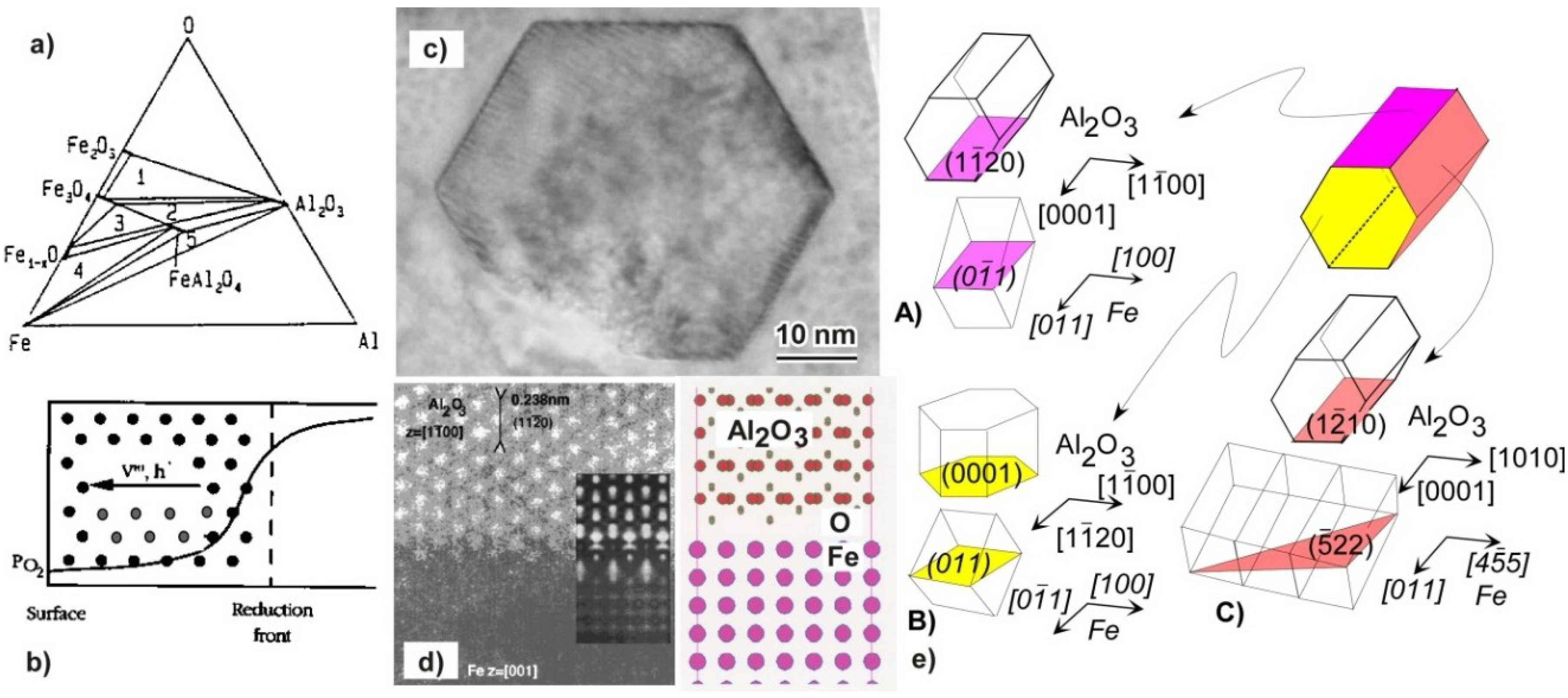
4.4. Fe/Al2O3 Interface: Model Experiment for Interface Bonds

The interface between iron and alumina was and is still an object of investigation because of its technological importance. We review here a model experiment, which was suggested for investigating atomistic studies at metal-ceramic interfaces in general. An Al2O3-Fe2O3 ceramic composite is annealed in a furnace, in which the Oxygen pressure is then gradually decreased. This so-called internal reduction [77] decreases the Oxygen partial pressure in such a way that metallic Fe and Al2O3 are stable, when region 5 in the phase diagram of Figure 7a is reached. The reaction starts from the surface, where the Oxygen is gradually reduced, and hence Fe particles are formed within the alumina matrix (Figure 7b) [78].
Figure 7. Experimental studies on the Fe/Al2O3 interface: (a) phase diagram; (b) oxygen diffusion and reaction front during internal reduction; (c) Fe-nano particle with prismatic shape within the Al2O3 matrix; (d) interface case (A) of (e) the three interfaces (AC) with their orientation relationships as confirmed by TEM.
Metals 04 00410 g007
As the precipitates grow slowly, their interfaces have reduced interface energy with facets parallel to low-index alumnia lattice planes (Figure 7c–e). The HRTEM micrograph of the interface A showed under certain focus conditions white dots in the alumina lattice and black dots in the Fe lattice, both could be matched to image simulations shown as in insert in Figure 7d. The results confirmed an O–Fe bond at the interface, while in the case of the Al2O3-Cr interface the Al-Cr bond is preferred [78]. Which case occurs depends on thermodynamic affinity.
Such experiments are important to find out the interatomic bonding at interfaces in order to control their properties. The opposite process of internal reduction is called internal oxidation. In a metallic alloy, the oxygen pressure is increased until of oxide particles within the metallic matrix are formed. This leads to special precipitation hardening of metals, while the internal reduced ceramics with their incorporated metal particles are used for example as ceramic cutting tools with increased wear resistance, toughening and durability.

4.5. Phenomena on Other Inorganic Interfaces

In functional materials, interfaces in general create a large change in properties, inorganic substances between materials with large dielectric constant (high-k) and with low-k [79] are of great importance for waveguides, laser diodes and other electronic devices. Such an example is the Al2O3/GaN interface [80], and structurally equivalent Alumina-Wurtzite-interfaces have been investigated as well. The lattice constants of GaN, AlN or ZnO are similar, as the behavior of anions and cations are. We report here MD-studies [81] on the Al2O3/ZnO interface [18] with the experimentally found relationship shown in Figure 8a. In both lattices, the base plane is facing each other, but with an in-plane rotation of 30°, as confirmed by XRD. The length of the supercell fits to the extended atomic distance, so that it contains one period of matching. In the case of zinc oxide five oxygen-oxygen bonds fits to six oxygen-oxygen bonding distance of Alumina in the cross section in Figure 8b. Starting from four models on atomic scale with different translation vectors, we found that all input structures finally yield to two configurations, one of them is shown in Figure 8b, in which Zn–O-tetrahedrons marked in red are pointing towards the interface. As ZnO is a ferro-electric material, we should emphasize that there is another configuration with opposite tetrahedron orientation, not shown here.
Figure 8. MD simulation results of the ZnO/Al2O3 interface: (a) orientation relationship; (b) cross sectional view; (c) planar view of interface region with three sets of misfit dislocations (b) reprinted with permission from publisher [18]).
Metals 04 00410 g008
The astonishing result of this MD simulation is that the interface structure consists of alternating units, in some parts the Al–O bond of alumina is formed marked by the blue units, in some parts the ZnO-bonds. In the planar view, we see that in the interface plane both units are co-existing. One explanation for this phenomenon was confirmed by studies on the free Alumina surface [81]. Whatever the initial start configuration is, always both Oxygen, and Aluminum atoms migrate to the surface, and maintain the charge neutrality at the surface. The model of the interface contains these structural units in periodical distances. Because at the interface of these two hexagonal lattices, the Corundum and Wurtzite structures are facing each other, misfit dislocations in three directions are present between these structural units and were confirmed in experimental studies [82].
Studies on functional interfaces improve semiconductor properties, such as Nb-doped SrTiO3with perovskite structure [83,84,85,86,87]. When during processing from TiO2 the amount of SrO is increased, natural nano-scaled Ruddlesden-Popper superlattices (SrTiO3)n(SrO)m are formed. At the interface, the (TiO6)2− octahedrons are slightly expanded, because SrO has lower electron density [86]. On the other hand, an artificial superlattice (SrTiO3)x/(SrTi1−zNbzO3)y increases the electron density [87]. As a consequence, the effective electron mass is increased, and hence, this material shows a giant Seebeck coefficient of S = 0.85 mV/K [49]. The mechanism is known as electron confinement in a two-dimensional electron gas (2DEG) occurring also at other thermoelectric composite materials with Perovskite structure [87,88,89,90]. We have found that similar phenomena are occurring also at half-Heusler phases, which was later reported in [91] without citation. (Ti,Zr)NiSn is a good thermoelectric bulk material with a fairly high Seebeck-coefficient of S = −0.25 mV/K [51,81,92,93]. When sputtering a thin film with a thickness of 1 μm on different substrates, the trend could be confirmed that the electron donating substrate Cu is beneficial for large Seebeck voltage [51]. The electric field at the p-/n-type interface is sucking electrons into the interface [49,51,86,89]. Further studies are needed to confirm which criteria are necessary for increasing the mobility and preventing recombination. The suggested mechanisms in controlling atomic structure of interfaces opens new possibilities in improving materials properties by interface engineering.

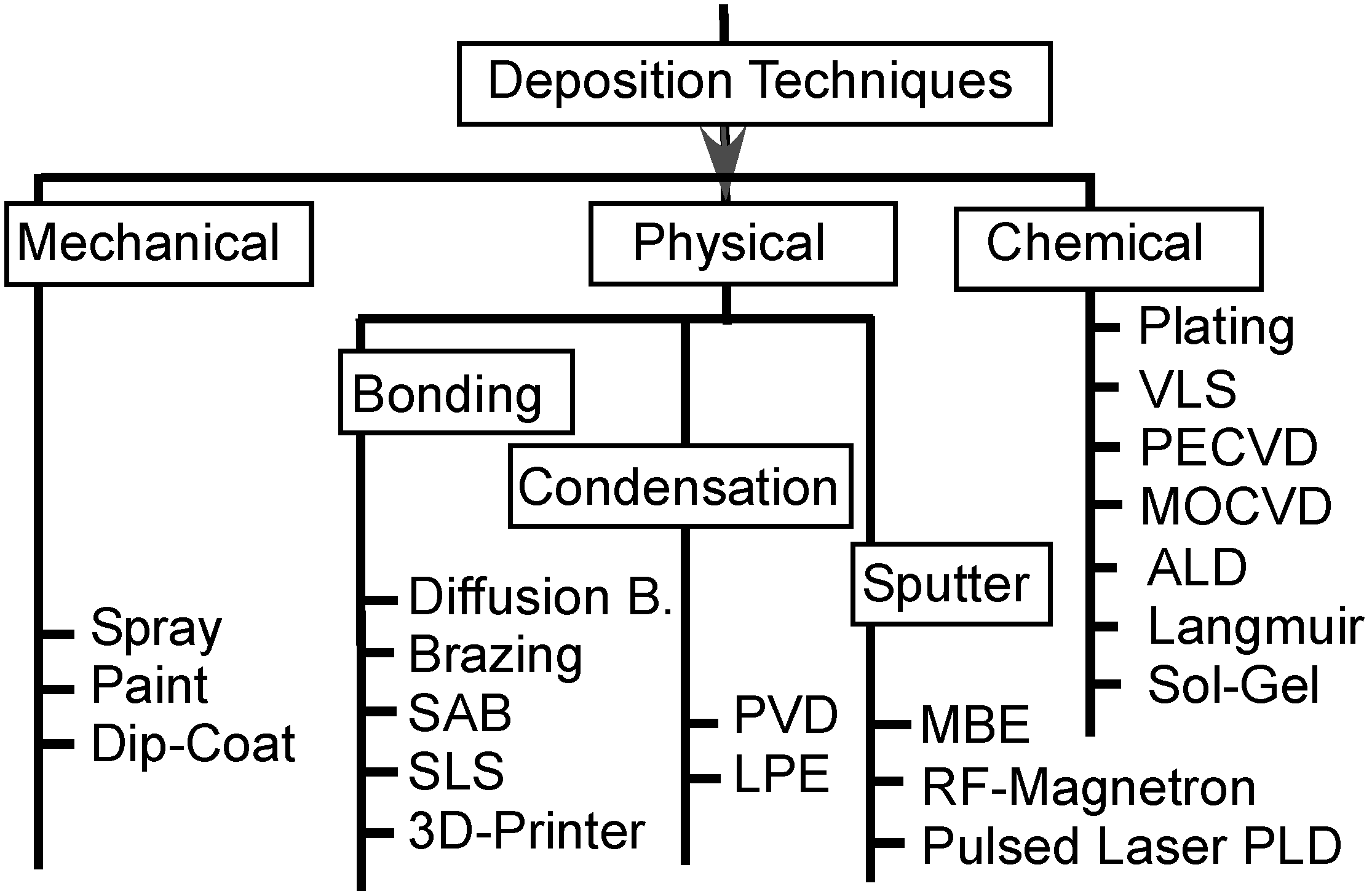
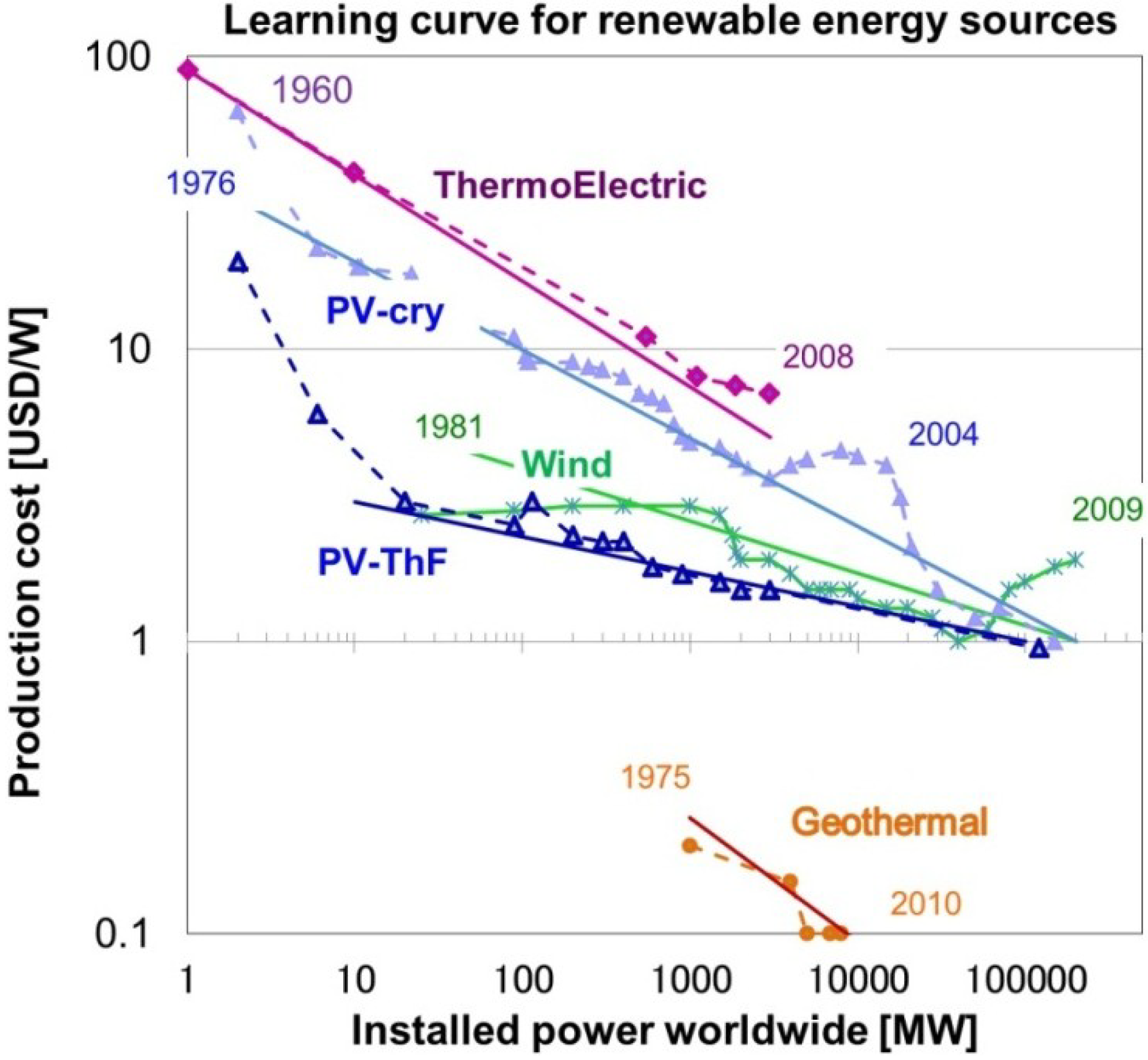
5. Outlook: Additive Manufacturing Allows Efficient Optimization of Device Interface

In this report, we have studied the atomic structure and properties of several interfaces. The interface is the smallest unit to build new functional materials or meta-materials with special designed properties superior to bulk materials. The implementation of innovative interface geometries is one of the central research topics for optimizing functional materials. When additive manufacturing becomes more popular, the demand for stable and functional interface research will grow. To develop the next-generation of environmental-friendly power generators these new possibilities provided by advanced thin film growth technologies and micro-fabrication technologies need to be utilized. There already exist reports of metal ceramic interfaces manufactured by a 3D printer [41,94,95].

6. Conclusions

This overview article describes atomistic studies of metal-ceramic interfaces.
(1)
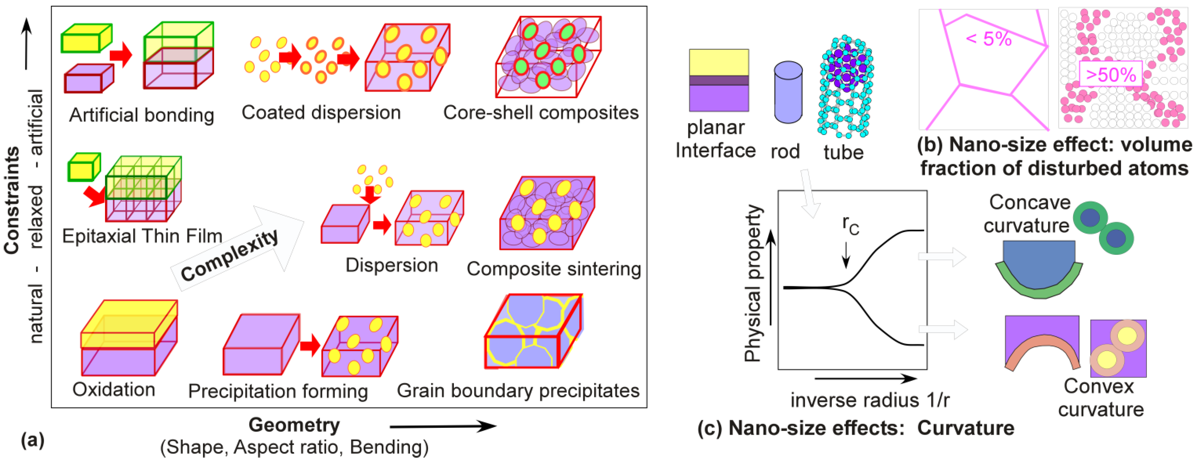
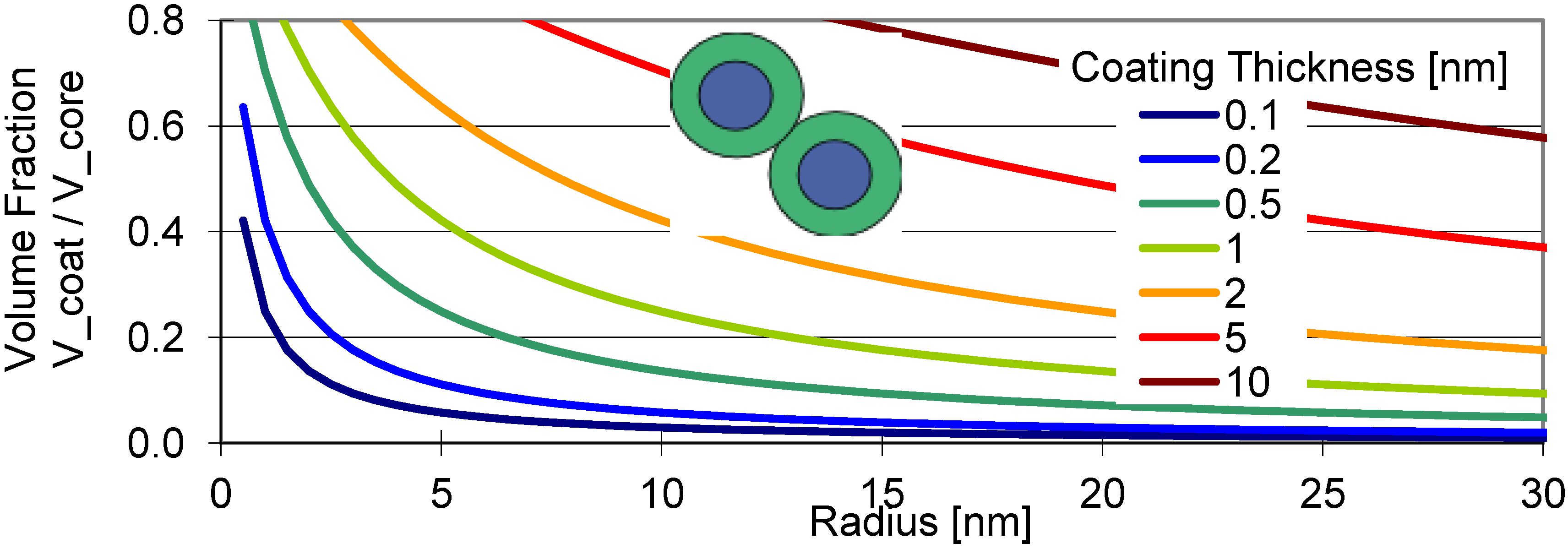
This field of science together with other inorganic interfaces will gain interest in the near future, because of three reasons: (a) thin film devices are cheaper than those made of bulk materials; (b) new additive manufacturing techniques are available; (c) nano-size effects, like the volume fraction of atoms in a crystalline environment and the curvature of interfaces, change properties of functional materials.in non-classical way. Complexity of heterogeneous interfaces can increase by two independent factors, either geometry or when producing interfaces far from equilibrium.
(2)
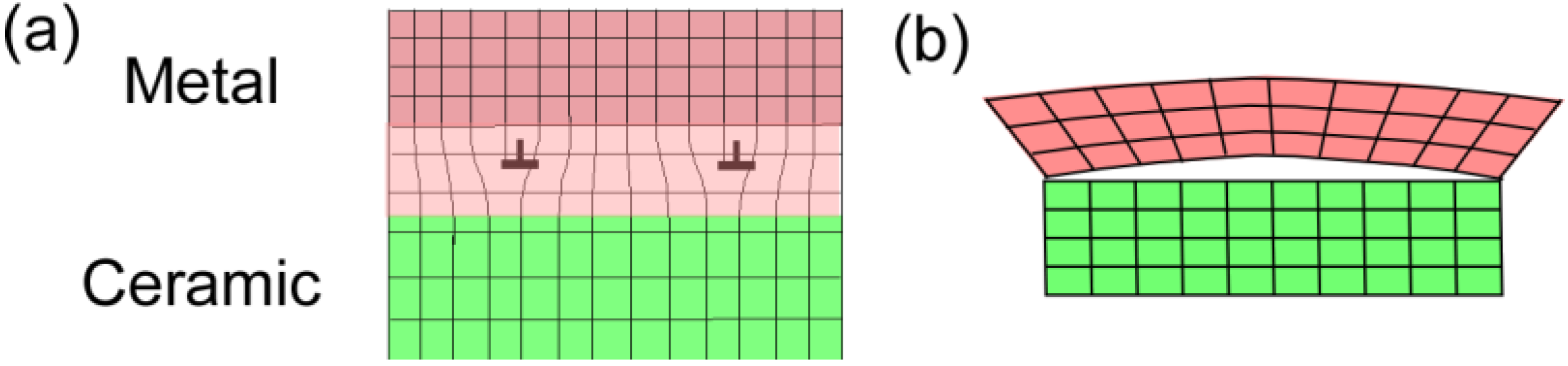
For atomistic modeling of crystalline interfaces, we need (a) to get the orientation between the facing lattices from experiments; (b) the translation vector of unit cells parallel and/or perpendicular to the interface; (c) individual relaxation of atomic positions forming structural units, which are different from units in bulk materials.
(3)
Experimental studies on several metal/ceramic and other interfaces confirmed their importance for future optimizing properties of either thin films on substrates, sandwich structures, or other composite materials. Epitaxial growth allows thin-film engineering by straining up to ±10%. At interfaces new structural units with unique bonding characteristics are formed.
(4)
The atomistic structure determines bonding and other properties, especially in functional materials the transport properties like 2DEG or GMR are influenced by new possibilities of the bonding partners. In addition, from the viewpoint of new additive manufacturing techniques such as 3D-printing of composites, compounds or their constituents, this field of science will see a large gain in importance in near future.

Acknowledgments

The author acknowledges useful discussions with Tadatomo Suga, at the University of Tokyo. Special thanks to the chief editor of MDPI, who invited the author to write this overview article.

Conflicts of Interest

The author declares no conflict of interest.

References

  1. Autumn, K.; Sitti, M.; Liang, Y.A.; Peattie, A.M.; Hansen, W.R.; Sponberg, S.; Kenny, T.W.; Fearing, R.; Israelachvili, J.N.; Full, R.J. Evidence for van der Waals adhesion in gecko setae. Proc. Natl. Acad. Sci. USA 2002, 99, 12252–12256. [Google Scholar] [CrossRef]
  2. Heepe, L.; Kovalev, A.E.; Filippov, A.E.; Gorb, S.N. Adhesion Failure at 180000 Frames per Second: Direct Observation of the Detachment Process of a Mushroom-Shaped Adhesive. Phys. Rev. Lett. 2013, 111, 104301. [Google Scholar] [CrossRef]
  3. Yurdumakan, B.; Raravikar, N.R.; Ajayanb, P.M.; Dhinojwala, A. Synthetic gecko foot-hairs from multiwalled carbon nanotubes. Chem. Commun. 2005, 3799–3801. [Google Scholar]
  4. Peisker, H.; Michels, J.; Gorb, S.N. Evidence for a material gradient in the adhesive tarsal setae of the ladybird beetle Coccinella septempunctata. Nat. Commun. 2013, 4, 1661. [Google Scholar] [CrossRef]
  5. Suga, T.; Hosoda, N. Active disassembly and reversible interconnection. Proc. IEEE Int. Symp. 2000. [Google Scholar] [CrossRef]
  6. Haisma, J.; Spierings, G.A.C.M. Contact bonding, including direct-bonding in a historical and recent context of materials science. Mater. Sci. Eng. R 2002, 37, 1–60. [Google Scholar] [CrossRef]
  7. Floriancic, M.; Mader, W.; Rühle, M.; Turwitt, M. HRTEM and diffraction studies on an Nb-Al2O3 interface. J. Phys. Colloques 1985, 46, C4:129–C4:133. [Google Scholar]
  8. Blöchl, P.; Das, G.P.; Fischmeister, H.F.; Schönberger, U. Electronic structure of a metal-ceramic interface: ab-initio calculations for MgO/Ag. Metal–Ceramic Interfaces 1990. [Google Scholar] [CrossRef]
  9. Schönberger, U.; Andersen, O.K.; Methfessel, M. Bonding at metal-ceramic interfaces; Ab-initio density-functional calculations for Ti and Ag on MgO. Acta Metall. Mater. 1992, 40, S1–S10. [Google Scholar] [CrossRef]
  10. Kohyama, M.; Ebata, Y.; Kose, S.; Kinoshita, M.; Yamamoto, R. Band-theoretical approach to bonding at metal-alumina interfaces. J. Phys. Colloq. 1990, 51, 861–866. [Google Scholar]
  11. Williamson, B.R.L.; Rabin, B.H.; Drake, J.T. Finite element analysis of thermal residual stresses at graded ceramic-metal interfaces. Part I. Model description and geometrical effects. J. Appl. Phys. 1993, 74, 1310. [Google Scholar]
  12. Peteves, S.D. Designing Interfaces for Technological Applications, Ceramic-Ceramic, Ceramic-Metal-Joining; Elsevier Applied Science: Amsterdam, The Netherlands, 1989. [Google Scholar]
  13. Wolf, D.; Yip, S. Material Interfaces; Champman & Hall: London, UK, 1992. [Google Scholar]
  14. Sutton, A.P.; Balluffi, R.W. Interfaces in Crystalline Materials; Clarendon Press: Oxford, UK, 1995. [Google Scholar]
  15. Rühle, M.; Evans, A.G.; Hirth, J.P.; Ashby, M.F. Metal–Ceramic Interfaces; Pergamon Press & Elsevier: Oxford, UK, 2009. [Google Scholar]
  16. Lojkowski, W.; Fecht, H.J. The structure of intercrystalline interfaces. Prog. Mater. Sci. 2000, 45, 339–568. [Google Scholar] [CrossRef]
  17. Ernst, F. Metal-oxide interfaces. Mater. Sci. Eng. R 1995, 14, 97–156. [Google Scholar] [CrossRef]
  18. Wunderlich, W. Ceramics Processing on Atomic Scale by Control of Interface Parameter. Interceram 2002, 51, 190–198. [Google Scholar]
  19. Wunderlich, W.; Niihara, K. Ab-initio Simulations in order to improve processing of Nanoceramics. J. Ceram. Proc. Res. 2003, 4, 10–16. [Google Scholar]
  20. Wunderlich, W.J. Calculations on different length scales for improving Processing of Nano-Ceramics Ceram. J. Ceram. Proc. Res. 2004, 5, 30–39. [Google Scholar]
  21. Wunderlich, W.; Oekermann, T.; Miao, L.; Hue, N.T.; Tanemura, S.; Tanemura, M. Electronic properties of Nano-porous TiO2- and ZnO-Thin Films comparison of simulations and experiments. J. Ceram. Proc. Res. 2004, 5, 343–354. [Google Scholar]
  22. Ertl, G.; Weiss, M.; Lee, S.B. Kinetics of nitrogen adsorption on Fe(111). Surf. Sci. 1982, 114, 515–526. [Google Scholar] [CrossRef]
  23. Ostrovskii, V.E. Review of the heats of chemisorption of gases at metals in the context of the problem of “Heterogeneous” vs. “Homogeneous” catalytic surfaces. J. Therm. Anal. Calorim. 2009, 95, 609–622. [Google Scholar] [CrossRef]
  24. Al-Abadleh, H.A.; Grassian, V.H. Oxide surfaces as environmental interfaces. Surf. Sci. Rep. 2003, 52, 63–161. [Google Scholar]
  25. Binasch, G.; Grünberg, P.; Saurenbach, F.; Zinn, W. Enhanced magnetoresistance in layered magnetic structures with antiferromagnetic interlayer exchange. Phys. Rev. B 1989, 39, 4828. [Google Scholar] [CrossRef]
  26. Baibich, M.N.; Broto, J.M.; Fert, A.; Nguyen van Dau, F.; Petroff, F.; Eitenne, P.; Creuzet, G.; Friederich, A.; Chazelas, J. Giant Magnetoresistance of (001)Fe/(001)Cr Magnetic Superlat-tices. Phys. Rev. Lett. 1988, 61, 2472. [Google Scholar] [CrossRef]
  27. Evans, A.G.; Mumm, D.R.; Hutchinson, J.W.; Meier, G.H.; Pettit, F.S. Mechanisms controlling the durability of thermal barrier coatings. Prog. Mater. Sci. 2001, 46, 505–553. [Google Scholar] [CrossRef]
  28. Chen, Y.; Reed, R.C.; Marquis, E.A. As-coated thermal barrier coating: Structure and chemistry. Scr. Mater. 2012, 67, 779–782. [Google Scholar] [CrossRef]
  29. Seiler, P.; Baker, M.; Roesler, J. Multi-scale failure mechanisms of thermal barrier coating systems. J. Comput. Mater. Sci. 2013, 80, 27–34. [Google Scholar] [CrossRef]
  30. Curry, N.; Markocsan, N.; Li, X.H.; Tricoire, A.; Dorfman, M. Next Generation Thermal Barrier Coatings for the Gas Turbine Industry. J. Therm. Spray Technol. 2011, 20, 108–115. [Google Scholar] [CrossRef]
  31. Arya, A.; Carter, E.A. Structure, bonding, and adhesion at the TiC(100)/Fe(110) interface from first principles. J. Chem. Phys. 2003, 118, 8982. [Google Scholar]
  32. Vepek, S. The search for novel, superhard materials. J. Vac. Sci. Technol. A 1999, 17, 2401. [Google Scholar] [CrossRef]
  33. Holec, D.; Friak, M.; Neugebauer, J.; Mayrhofer, P.H. Trends in the elastic response of binary early transition metal nitrides. Phys. Rev. B 2012, 85, 064101. [Google Scholar] [CrossRef]
  34. Rachbauer, R.; Gengler, J.J.; Voevodin, A.A.; Resch, K.; Mayrhofer, P.H. Temperature driven evolution of thermal, electrical, and optical properties of Ti-Al-N coatings. Acta Mater. 2012, 60, 2091–2096. [Google Scholar] [CrossRef]
  35. Mayrhofer, P.H.; Sonnleitner, D.; Bartosik, M.; Holec, D. Sructural and mechanical evolution of reactively and non-reactively sputtered Zr–Al–N thin films during annealing. Surf Coat Technol. 2014, 244, 52–56. [Google Scholar] [CrossRef]
  36. Knoth, K.; Engel, S.; Apetrii, C.; Falter, M.; Schlobach, B.; Hühne, R.; Oswald, S.; Schultz, L.; Holzapfel, B. Chemical solution deposition of YBa2Cu3O7−x coated conductors. Curr. Opin. Solid State Mater. Sci. 2006, 10, 205–216. [Google Scholar]
  37. Suga, T. Low Temperature Bonding for 3D Integration—A Review of the Surface Activated Bonding (SAB). In proceedings of Low Temperature Bonding for 3D Integration (LTB-3D), 2012 3rd IEEE International Workshop on, Tokyo, Japan, 22–23 May 2012; pp. 7–10.
  38. Howlader, M.M.R.; Zhang, F.; Deen, M.J.; Suga, T.; Yamauchi, A. Surface activated bonding of copper through silicon vias and gold stud bumps at room temperature. J. Vac. Sci. Technol. A 2011, 29, 021007. [Google Scholar]
  39. Wilk, G.D.; Wallace, R.M.; Anthony, J.M. High-k gate dielectrics: Current status and materials properties considerations. J. Appl. Phys. 2001, 89, 5243–5275. [Google Scholar] [CrossRef]
  40. Fu, Q.; Wagner, T. MOS field-effect transistor gate and in heterogeneous catalysis. Surf. Sci. Rep. 2007, 62, 431–498. [Google Scholar]
  41. Imanaka, Y.; Amada, H.; Kumasaka, F.; Takahashi, N.; Yamasaki, T.; Ohfuchi, M.; Kaneta, C. Nanoparticulated dense and stress-free ceramic thick film for material integration. Adv. Eng. Mater. 2013, 15, 1129–1135. [Google Scholar]
  42. Falub, C.V.; Känel, H.V.; Isa, F.; Bergamaschini, R.; Marzegalli, A.; Chrastina, D.; Isella, G.; Müller, E.; Niedermann, P.; Miglio, L. Scaling Hetero-Epitaxy from Layers to Three-Dimensional Crystals. Science 2012, 335, 1330–1334. [Google Scholar] [CrossRef] [Green Version]
  43. Nomura, K.; Ohta, H.; Ueda, K.; Kamiya, T.; Hirano, M.; Hosono, H. Thin-film transistor fabricated in single-crystalline transparent oxide semiconductor. Science 2003, 300, 1269–1272. [Google Scholar] [CrossRef]
  44. Fortunato, E.; Barquinha, P.; Martins, R. Oxide Semiconductor Thin-Film Transistors: A Review of Recent Advances. Adv. Mater. 2012, 24, 2945–2986. [Google Scholar] [CrossRef]
  45. Furubayashi, Y.; Hitosugi, T.; Yamamoto, Y.; Inaba, K.; Kinoda, G.; Hirose, Y.; Shimada, T.; Hasegawa, T. A transparent metal: Nb-doped anatase TiO2. Appl. Phys. Lett. 2005, 86, 252101. [Google Scholar] [CrossRef]
  46. Hautier, G.; Miglio, A.; Ceder, G.; Rignanese, G.-M.; Gonze, X. Identification and design principles of low hole effective mass p-type transparent conducting oxides. Nat. Commun. 2013, 4, 2292. [Google Scholar]
  47. Ekins-Daukes, N.J.; Lee, K.-H.; Hirst, L.; Chan, A.; Führer, M.; Adams, J.; Browne, B.; Barnham, K.W.J.; Stavrinou, P.; Connolly, J.; et al. Controlling radiative loss in quantum well solar cells. J. Phys. D 2013, 46, 264007:1–264007:8. [Google Scholar]
  48. Snyder, G.J.; Lim, J.R.; Huang, C.K.; Fleurial, J.P. Thermoelectric microdevice fabricated by a MEMS-like electrochemical process. Nat. Mater. 2003, 2, 528–531. [Google Scholar]
  49. Ohta, H.; Kim, S.; Mune, Y.; Mizoguchi, T.; Nomura, K.; Ohta, S.; Nomura, T.; Nakanishi, Y.; Ikuhara, Y.; Hirano, M.; et al. Giant thermoelectric Seebeck coefficient of a two-dimensional electron gas in SrTiO3. Nat. Mater. 2007, 6, 129–134. [Google Scholar]
  50. Takashiri, M.; Shirakawa, T.; Miyazaki, K.; Tsukamoto, H. Fabrication and characterization of bismuth–telluride-based alloy thin film thermoelectric generators. Sens. Actuators A 2007, 138, 329–334. [Google Scholar] [CrossRef]
  51. Wunderlich, W.; Shinohara, Y.; Matsumura, Y. Magnetron sputtering of (TiZr)NiSn thin films on different substrates for thermoelectric applications. J. Phys. 2012, 379. [Google Scholar] [CrossRef]
  52. Wunderlich, W.; Takashiri, M.; Wakaki, M. Energy Harvesting by Thermoelectric Materials—Thin Film Development and Characterization. Proc. Sch. Eng. Tokai Univ. 2012, 52, 45–50. [Google Scholar]
  53. Sluka, T.; Tagantsev, A.K.; Bednyakov, P.; Setter, N. Free-electron gas at charged domain walls in insulating BaTiO3. Nat. Commun. 2013, 4, 1808. [Google Scholar] [CrossRef]
  54. Felser, C.; Fecher, G.H.; Balke, B. Spintronics: A Challenge for Materials Science and Solid-State Chemistry. Angew. Chem. Int. Ed. 2007, 46, 668–699. [Google Scholar] [CrossRef]
  55. Tian, Y.F.; Ding, J.F.; Lin, W.N.; Chen, Z.H.; David, A.; He, M.; Hu, W.J.; Chen, L.; Wu, T. Anomalous exchange bias at collinear/noncollinear spin interface. Nat. Sci. Rep. 2012, 3, 1094. [Google Scholar]
  56. Harmer, M.P. The Phase Behavior of Interfaces. Science 2011, 332, 182–183. [Google Scholar] [CrossRef]
  57. Luo, J.; Cheng, H.; Asl, M.K.; Kiely, C.J.; Harmer, M.P. The Role of a Bilayer Interfacial Phase on Liquid Metal Embrittlement. Science 2011, 332, 1730–1733. [Google Scholar]
  58. Wunderlich, W.; Mori, T.; Sologub, O.; Baufeld, B. SPS-Sintering of NaTaO3-Fe2O3 Composites. J. Aust. Ceram. Soc. 2011, 47, 57–60. [Google Scholar]
  59. Chookajorn, T.; Murdoch, H.A.; Schuh, C.A. Design of Stable Nanocrystalline Alloys. Science 2012, 337, 951–953. [Google Scholar] [CrossRef]
  60. Wunderlich, W.; Ishida, Y.; Maurer, R. HRTEM-Studies of the microstructure of nano-crystalline Pd. Scr. Metall. Mater. 1990, 24, 403–408. [Google Scholar] [CrossRef]
  61. Wunderlich, W.; Takahashi, M. Characterization of nano-particles during Mg-Al-Spinel-Formation. Ceram. Trans. 2010, 133, 189–194. [Google Scholar]
  62. Wunderlich, W.; Hue, N.T.; Tanemura, S. Fabrication of nano-structured Titania-Thin-Films. AZojomo 2006, 2, 208. [Google Scholar]
  63. Han, H.; Kim, Y.; Alexe, M.; Hesse, D.; Lee, W. Nanostructured Ferroelectrics: Fabrication and Structure–Property Relations. Adv. Mater. 2011, 23, 4599–4613. [Google Scholar] [CrossRef]
  64. Gangopadhyay, S.; Hadjipanayis, G.C.; Shah, S.I.; Sorensen, C.M.; Klabunde, K.J.; Papaefthymiou, V.; Kostikas, A. Effect of oxide layer on the hysteresis behavior of fine Fe particles. J. Appl. Phys. 1991, 70, 5888–5890. [Google Scholar] [CrossRef]
  65. Kolen’ko, Y.V.; Bañobre-López, M.; Rodríguez-Abreu, C.; Carbó-Argibay, E.; Sailsman, A.; Piñeiro-Redondo, Y.; Cerqueira, F.M.; Petrovykh, D.Y.; Kovnir, K.; Lebedev, O.I.; et al. Large-Scale Synthesis of Colloidal Fe3O4 Nanoparticles Hyperthermia. J. Phys. Chem. C 2014, 118, 8691–8701. [Google Scholar] [CrossRef]
  66. Wunderlich, W.; Fujimoto, M.; Ohsato, H.; Sekiguchi, S.; Suzuki, T. MD simulation about misfit dislocations at the BaTiO3/SrTiO3 interface. Thin Solid Films 2000, 375, 9–14. [Google Scholar] [CrossRef]
  67. Lopez, N.; Valeri, S. MgO/Ag 001 interface structure and ST images from first principles. Phys. Rev. B 2004, 70, 125428. [Google Scholar] [CrossRef]
  68. Shibata, N.; Okubo, S.; Saito, Y.; Wunderlich, W.; Ikuhara, Y. Formation of Cubic-AlN Layer on MgO (100) Substrate by Ion-Assisted MBE. In Proceedings of 7th International Conference on Nitride SemiconductorsFine Ceramic Center, Tokushima, Japan, 27 October 1997; pp. 374–377.
  69. Wunderlich, W.; Kremser, T.; Frommeyer, G. Mobile Dislocations at Phase Boundaries in Intermetallic TiAl/Ti3Al-Alloys. Acta Metall. Mater. 1993, 41, 1791–1799. [Google Scholar] [CrossRef]
  70. Wunderlich, W.; Frommeyer, G.; Czarnowski, P.V. Arrangement of Misfit Dislocations at TiAl/Ti3Al-Phase Boundaries. Mater. Sci. Eng. 1993, A164, 421–427. [Google Scholar] [CrossRef]
  71. Wunderlich, W.; Miao, L.; Tanemura, M.; Tanemura, S.; Jin, P.; Kaneko, K.; Terai, A.; Nabatova-Gabin, N.; Belkada, R. Ab inito Calculations of the optical Bandgap of TiO2 Thin Films. Int. J. Nanosci. 2004, 3, 439–445. [Google Scholar]
  72. Tanemura, S.; Miao, L.; Wunderlich, W.; Tanemura, M.; Mori, Y.; Toh, S.; Kaneko, K. Fabrication and characterization of anatase/rutile–TiO2 thin films by magnetron sputtering: A review. Sci. Technol. Adv. Mater. 2005, 6, 11–17. [Google Scholar] [CrossRef]
  73. Wunderlich, W.; Miao, L.; Tanemura, S.; Tanemura, M. Suitable substrates for rutile TiO2-thin films with narrow band-gap predicted by calculations on atomic scale. In Proceedings of the International Conference on New Frontiers of Process Science and Engineering in Advanced Materails—The 14th Iketani Conference, Kyoto, Japan, 24–26 November 2005; Naka, M., Yamane, T., Eds.; High Temperature Society of Japan: Osaka, Japan, 2005; pp. 1–6. [Google Scholar]
  74. Choudhury, S.; Betty, C.A. A heterostructured SnO2–TiO2 thin film prepared by Langmuir–Blodgett technique. Mater. Chem. Phys. 2013, 141, 440–444. [Google Scholar]
  75. Siripala, W.; Ivanovskaya, A.; Jaramillo, T.F.; Baeck, S.H. A Cu2O/TiO2 heterojunction thin film cathode for photoelectrocatalysis. Sol. Energy Mater. Sol. Cells 2003, 77, 229–237. [Google Scholar] [CrossRef]
  76. Polat, Ö.; Aytug, T.; Lupini, A.R.; Paranthaman, P.M.; Ertugrul, M.; Bogorin, D.F.; Meyer, H.M.; Wang, W.; Pennycook, S.J.; Christen, D.K. Nanostructured columnar heterostructures of TiO2 and Cu2O enabled by a thin-film self-assembly approach: Potential for photovoltaics. Mater. Res. Bull. 2013, 48, 352–356. [Google Scholar] [CrossRef]
  77. Backhaus-Ricoult, M.; Hagège, S.; Peyrot, A.; Moreau, P. Internal Reduction of Chromium-Doped α-Alumina. J. Am. Cerams. Soc. 1994, 77, 423–430. [Google Scholar] [CrossRef]
  78. Backhaus-Ricoult, M.; Hagège, S.; Wunderlich, W.; Peyrot, A. Atomic Structure of precipitate interfaces of bcc metals. In Alumina formed by internal reduction, Proceedings of International Conference on Ceramic Microstructures, Berkeley, CA, USA, 24 June 1996; pp. 1–10.
  79. Först, C.J.; Ashman, C.R.; Schwarz, K.; Blöchl, P.E. The interface between silicon and a high-k oxide. Nature 2004, 427, 53–56. [Google Scholar] [CrossRef]
  80. Kato, T.; Kung, P.; Saxler, A.; Sun, C.J.; Ohsato, H.; Razeghi, M.; Okuda, T. Simultaneous growth of two differently oriented GaN epilayers on (1 1 • 0) sapphire II. A growth model of (0 0 • 1) and (10 • 0) GaN. J. Cryst. Growth 1998, 183, 131–139. [Google Scholar] [CrossRef]
  81. Wunderlich, W.; Awaji, H. Molecular Dynamics Simulations of the fracture toughness of Sapphire. Mater. Des. 2001, 22, 53–59. [Google Scholar] [CrossRef]
  82. Dimitrakopulos, G.P.; Komninou, P.; Pond, R.C. Topological Analysis of Defects in Epitaxial Nitride Films and Interfaces. Phys. Stat. Sol.(b) 2001, 227, 45–92. [Google Scholar] [CrossRef]
  83. Wunderlich, W.; Ohta, H.; Koumoto, K. Enhanced effective mass in doped SrTiO3 and related perovskites. Phys. B 2009, 404, 2202–2212. [Google Scholar] [CrossRef]
  84. Wunderlich, W.; Koumoto, K. Development of high-temperature thermoelectric materials based on SrTiO3-layered perovskites. Int. J. Mater. Res. 2006, 97, 657–662. [Google Scholar]
  85. Wunderlich, W. Reduced bandgap due to phonons in SrTiO3 analyzed by ab-initio calculations. Solid State Electron. 2008, 52, 1082–1087. [Google Scholar] [CrossRef]
  86. Wunderlich, W.; Ohta, S.; Ohta, H.; Koumoto, K. Effective mass and thermoelectric properties of SrTiO 3-based natural superlattices evaluated by ab-initio calculations. In proceedings of 24th International Conference on Thermoelectrics, Clemson University, SC, USA, 19–23 June 2005; IEEE: Piscataway, NJ, USA, 2005; pp. 252–255. [Google Scholar]
  87. Wunderlich, W.; Ohta, H.; Koumoto, K. Effective mass calculations of SrTiO3-based superlattices for thermoelectric applications lead to new layer design. Mater. Sci. 2008. [Google Scholar]
  88. Wunderlich, W. NaTaO3 composite ceramics—A new thermoelectric material for energy generation. J. Nucl. Mater. 2009, 389, 57–61. [Google Scholar] [CrossRef]
  89. Wunderlich, W.; Baufeld, B. Chapter 1: Development of Thermoelectric materials based on NaTaO3 –composite ceramics. In Ceramic Materials; Wunderlich, W., Ed.; InTech Publisher: Rijeka, Croatia, 2010; pp. 1–27. [Google Scholar]
  90. Wunderlich, W.; Fujiwara, H. The Difference between thermo- and pyroelectric Co-based RE-(= Nd, Y, Gd, Ce)-oxide composites measured by high-temperature gradient. J. Electron. Mater. 2011, 40, 127–133. [Google Scholar] [CrossRef]
  91. Graf, T.; Felser, C.; Parkin, S.S. Simple rules for the understanding of Heusler compounds. Prog. Solid. State. Chem. 2011, 39, 1–50. [Google Scholar]
  92. Wunderlich, W.; Motoyama, Y. Screening and Fabrication of Half-Heusler phases for thermoelectric applications. MRS Proc. 2009, 1128, 1–6. [Google Scholar]
  93. Wunderlich, W.; Motoyama, Y.; Sugisawa, Y.; Matsumura, Y. Large Seebeck Closed-Circuit Currents in Quaternary (Ti,Zr)NiSn Heusler-Alloys. J. Electron. Mater. 2011, 40, 583–588. [Google Scholar] [CrossRef]
  94. Santos, E.C.; Shiomi, M.; Osakada, K.; Laoui, T. Rapid manufacturing of metal components by laser forming. Int. J. Mach. Tools Manuf. 2006, 46, 1459–1468. [Google Scholar] [CrossRef]
  95. Levi, G.N.; Schindel, R.; Kruth, J.P. Rapid manufacturing and rapid tooling with layer manufacturing (LM) technologies, state of the art and future perspectives. CIRP Ann. Manuf. Technol. 2003, 52, 589–609. [Google Scholar] [CrossRef]

