Article

Effects of Reflow Time on the Interfacial Microstructure and Shear Behavior of the SAC/FeNi-Cu Joint

1
School of Mechanical and Electrical Engineering, Shanghai Dianji University, Shanghai 201306, China
2
School of Material and Science Engineering, Jiangsu University of Science and Technology, Zhenjiang 212003, China
*
Author to whom correspondence should be addressed.
Metals 2016, 6(5), 109; https://doi.org/10.3390/met6050109
Submission received: 21 March 2016 / Revised: 26 April 2016 / Accepted: 28 April 2016 / Published: 11 May 2016

Abstract

:
Effects of reflow time on the interfacial microstructure and shear strength of the SAC/FeNi-Cu connections were investigated. It was found that the amount of Cu6Sn5 within the solder did not have a noticeable increase after a long time period of reflowing, indicating that the electro-deposited FeNi layer blocked the Cu atoms effectively into the solder area during a long period under liquid-conditions. The ball shear test results showed that the SAC/FeNi-Cu joint had a comparable strength to the SAC/Cu joint after reflowing, and the strength drop after reflowing for 210 s was less than that of the SAC/Cu joint.
Keywords:
FeNi; UBM; IMCs

Graphical Abstract

1. Introduction

Solder bump connection is an important interconnect in flip chip packages, where the solder bumps deposited on metal terminals on the chip are connected to the metal pads on the substrate [1]. The metal terminals consist of successive layers of metal, under bump metal (UBM), which provides a strong mechanical and electrical connection. It is often regarded as a metallurgical process because of the formation of intermetallic compounds (IMCs) [2,3]. Cu film is widely used as a UBM or soldering pad because of its outstanding wetting property, conductivity and cheapness. However, the Cu film is consumed too quickly in the liquid reaction with solder bump alloy during reflow and the solid thermal aging process. Therefore, a barrier film such as Ni-P layer is utilized to protect the excessive loss of Cu film [4,5,6]. However, the existence of Kirkendall voids around the solder/Ni interface and the P-rich layer formations can degrade the reliability of the connection dramatically. To some extent, the thinner IMC layer has been realized to be an effective approach to improve the reliability of the interconnections.
FeNi alloy has been widely applied in precision instruments and used as lead-frame materials due to its excellent low-expansion property. Early studies on the Fe-Ni alloy are mainly about the brazing or solid bonding processes. Recently, a few publications have reported on the interfacial reactions between Sn based solders and Fe-Ni alloys, discussing its potential application as UBM layer for Sn-based solders [7,8,9,10,11,12,13,14,15,16]. It is reported that the FeNi layer has an acceptable wettability for SnAgCu (SAC) solder with or without an adequate pre-treatment in soldering [7], exhibiting a slower interfacial reaction rate compared to the traditional UBMs [8]. Moreover, the shear resistance behavior of an SAC solder joint can be slightly improved by using the FeNi alloy rather than the Cu substrate [9,10]. Moreover, it is found that only FeSn2 phase with minor Ni solubility formed between the FeNi substrate and Sn solder during liquid reactions at 270 °C [11,12,13,14]. Subsequently, the IMC formed at the Sn/FeNi interface was shown to be very sensitive to the concentration of Ni in FeNi alloys [15], and could transformed from (Ni,Fe)3Sn4 into FeSn2 phase when the Fe content in the Fe-Ni layer was between 10% to 12.5% [16]. The Sn-Bi and Sn-Cu eutectic solders reacted with the Fe-Ni substrate. Yen et al. revealed that only the FeSn2 phase was formed at the interfacial reactions [17]. In this study, the interfacial stability during reflow for different time periods was implemented. The microstructure and the shear properties of SAC/FeNi-Cu connection were investigated to discuss the potential application of FeNi layer as UBM layer for a Sn-based solder.

2. Experiments

The FeNi film surface was electro-deposited on a copper substrate with the atomic ratio of Fe:Ni near to 24:76 by adjusting the composition of the plating solution. The single lap shear joints of Cu/SAC/Cu (eutectic SAC solder) and Cu-FeNi/SAC/FeNi-Cu were fabricated using a solder ball of SAC alloy about 1 mm in diameter. The reflow process was executed on a BGA rework station at 260 °C for different time: 90, 150, 210 and 270 s respectively. Lap shear tests were carried out on a micromechanical testing system at a displacement control of 0.4 mm/min. The interfacial microstructures and the fracture surfaces after shear were observed by Scanning Electron Microscopy (SEM, Leica Cambridge, Cambridge, UK) and Energy Dispersive X-ray Spectroscopy (EDS, Shimadzu, Kyoto, Japan).

3. Results and Discussion

3.1. Interfacial Microstructure After Reflow

Figure 1 shows the surface morphology of FeNi film as deposition, a mirror like appearance. None is detected on gross or microscopic examination. Further EDS results, namely the semi-quantitative analysis, shows that element Fe in the prepared film is 25 at. %, see Figure 1b.
Figure 2 displays the cross-sectional images of the interfaces between SAC solder and substrates. A scallop IMC layer can be seen in Figure 2a along the SAC/Cu interface, mainly showing the Cu6Sn5 phase indicated by EDS analysis. The peak thickness of the scallop morphology IMC was above 5 μm. When the SAC solder reacted with the deposited FeNi film under the same conditions, by contrast, a flat and thin IMC in sub-micrometer thickness was formed at the interface of SAC and the FeNi layer, see Figure 2b. This planar IMC was very thin, about 180 nm, indicating that the consumption rate of FeNi film was enormously slow compared with the Cu substrate during the reflow process.
Based on the results regarding SAC/FeNi-Cu and SAC/FeNi from Guo and Hwang [7,14], this very thin IMC was determined to be FeSn2 phase with a tetragonal crystal structure determined by Zhu at the same 260 °C reflowing conditions [9]. It is completely in accordance with our previous results on the liquid reaction between Sn based solder and FeNi substrate [18], where Sn reacts with Fe preferentially over Ni.

3.2. Interfacial Microstructures After Reflowing for Different Time

During the reflowing processes at 260 °C, it was found that the total IMC thickness of Cu6Sn5 between SAC solder and substrate Cu grew thicker with the reflow time prolonged from 90 to 270 s (see Figure 3). At such a high temperature, Cu atoms easily diffused into SAC solder, and firstly reacted with Sn at the SAC/Cu interface to form Cu6Sn5 IMC. Along with this, Cu atoms also diffused into the inner SAC solder and formed irregular Cu6Sn5 phase. During the process, no other IMC phases (i.e., Cu3Sn emerging during the solid state aging) showed in the reflow time-increasing procedure for the formation needing longer incubation time [19]. The scallop morphology of Cu6Sn5 also remained.
For comparison, the IMC thickness between the SAC solder and the FeNi substrate did not show any obvious increase, as shown in Figure 4a–d. The thickness still kept blow 0.5 μm even after reflowing for almost 270 s. Moreover, the IMC type at the FeNi-Cu/SAC interface remained the single FeSn2 phase.
It is worth noting that the FeSn2 phase remains unchanged between the FeNi-Cu/SAC interface. Only the microstrucutre around the interface is slightly different. In Figure 4b, for example, the element Ni from UBM diffused into the solder rather than producing Ni-Sn IMC phase near the interface. The EDS result in Table 1 showed that some of the Cu6Sn5 phase within solder near the interface turned out to be Cu6Sn5 containing Ni, i.e., (Cu,Ni)6Sn5, where some places of Cu atoms in Cu6Sn5 crystalline lattice were occupied by the Ni atoms [20].
With increasing reflow time, the Ni diffused in the solder and formed an Ni-containing Cu6Sn5 compound, which made the area near the interface getting coarser. We even observed spalling away from the interface like a band when reflowing time was prolonged to 270 s, see Figure 4c,d. The further line scanning and EDS result showed that this IMC could also be the Ni-containing Cu6Sn5.
For SAC/Cu joints, the amount of Cu6Sn5 phase was much larger with increasing reflow time. This means that the excessive Cu came from the Cu substrate during the reflowing process. In comparison, for SAC/FeNi-Cu joints, the amount of Cu6Sn5 within the solder did not have a noticeable increase after a long time period of reflowing, indicating that the electro-deposited FeNi layer blocked the Cu atoms effectively into the solder during a long time stay in liquid conditions.

3.3. IMCs Growth Depending on Reflow Time

The dependence of the IMCs thickness on reflow time for the SAC/Cu and SAC/FeNi-Cu joints are shown in Figure 5. It can be seen that the IMCs thickness increases almost linearly with prolonged reflow time, which is quite different from the results reported in [17], a parabola relationship. This difference might be caused by different internal mechanisms of IMC growth during the liquid/solid process. Generally, the growth of the IMCs between the solder and the UBM are regarded as a reaction and diffusion controlled process. During this process, a new IMC phase may form resulting from the chemical reaction between the liquid solder and the solid UBM. Thus, the elements required to create the new phase may diffuse from the UBM and solder respectively across the IMC to the other side. Under a certain temperatures, the reaction layers grow, depending on the evolution of IMCs in the interface. Therefore, the whole process can be co-accomplished by the surface chemical reaction and the internal atoms diffusion mechanisms. Here, d can be used to show the growth of the IMC phase, then its relationship with time can be expressed as: d = (kt)n. Among them, k is the growth rate constant of the IMC layer, t is the IMC growth time, and n is the time index. When the compound growth is controlled by surface chemical reaction, the increase of the compound thickness with time prolonging should be a linear relationship (n = 1). When the reaction required elemental atoms diffusion dominates the compound growth, a parabola relationship between d and t begin to play a role (n = 0.5). From the results in Figure 5, the k values of growth rate could be calculated as 3.5 × 10⁻⁹ and 3.4 × 10⁻¹ m·s−1 for the SAC/Cu and SAC/FeNi-Cu joints respectively at 260 °C. For the SAC/FeNi-Cu joint, because the element Fe acted as the dominant reaction element forming the interfacial FeSn2 IMC. It can be deduced that the reaction rate of FeSn2 phase formation are ten times slower than the Cu-Sn compound. Also, the FeNi layer prevented the Cu from forming Cu6Sn5 IMC along the interface.

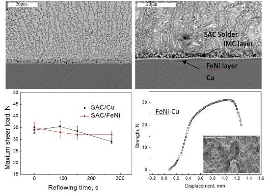
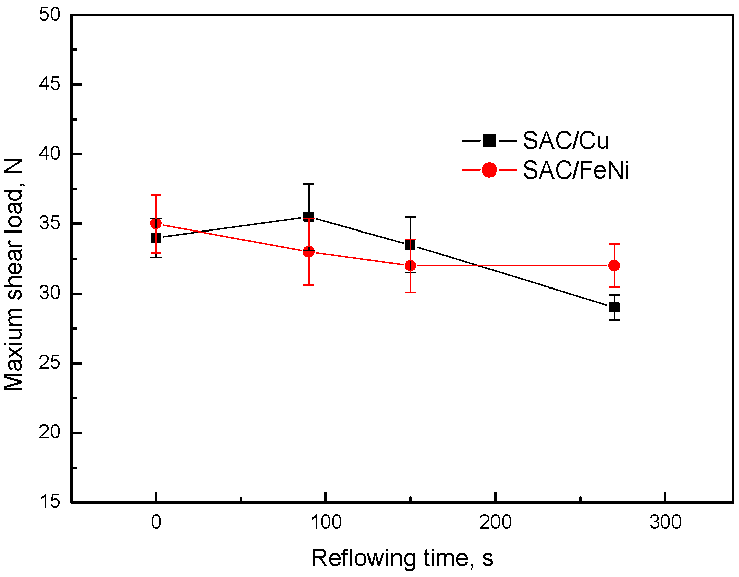
3.4. Shear Properties and the Fracture Behavior

As shown in Figure 6, the maximum shear strength occurred at the joints reflowed for 90 s for the SAC/Cu and SAC/FeNi-Cu joints. It can be seen that both joints had a comparable strength during the reflow time range from 90 to 270 s. After reflowing for 90 s, the strength of SAC/Cu dropped as the reflow time increased, especially at the initial stage. Comparatively, the strength of the SAC/FeNi-Cu joint had a slight decrease after a short reflow time, and then remained almost constant as reflow time increased. This result showed that the SAC/FeNi-Cu joints were less sensitive to the reflow time.
The relationship between the shear strength and the shear displacement for the SAC/Cu and SAC/FeNi-Cu joints reflowed at 260 °C for 270 s and the corresponding fracture surface observations are displayed in Figure 7. The fracture surfaces of both joints showed a mixture feature of ductile dimples and shear bands within the solders. In general, the fracture mode of the SAC/FeNi-Cu joint presented a more ductile process and represented a much higher mechanical reliability than the fractures within or between the different IMC layers or along the IMC/substrate interface. This result indicated that the SAC/FeNi-Cu joint had a better mechanical reliability after a long time period of reflowing at 260 °C.

4. Conclusions

During reflowing, a very thin FeSn2 IMC layer was formed at the SAC/FeNi-Cu interface. The growth rate of the FeSn2 layer was much lower than that of the Cu-Sn IMC at the SAC/Cu interface with prolonged reflow time. This indicated that the electro-deposited FeNi layer could effectively block the Cu atom diffusion into the solder during a much longer time period under liquid conditions. The solder lap shear test showed that the SAC/FeNi-Cu connection had an acceptable mechanical reliability after a long time period of reflowing at 260 °C.

Acknowledgments

This work was supported by special foundation of Shanghai Economic and Information Commission, No. JJ-YJCX-01-15-5718, Zhongche Nanjing Puzhen Vehicle Co. Ltd., No. C022.

Author Contributions

Yunxia Chen conceived and designed the experiments, analyzed the data and wrote the paper; Xulei Wu and Xiaojing Wang performed the experiments; Hai Huang contributed analysis tools.

Conflicts of Interest

The authors declare no conflict of interest.

References

  1. Wong, C.P.; Luo, S.J.; Zhang, Z.Q. Microelectronics: Flip the Chip. Science 2000, 290, 2269–2270. [Google Scholar] [CrossRef] [PubMed]
  2. Ho, C.E.; Yang, S.C.; Kao, C.R. Interfacial reaction issues for lead-free electronic solders. J. Mater. Sci. 2007, 18, 155–174. [Google Scholar]
  3. Laurila, T.; Vuorinen, V.; Kivilahti, J.K. Interfacial reactions between lead-free solders and common base materials. Mater. Sci. Eng. R 2005, 49, 1–60. [Google Scholar] [CrossRef]
  4. Ghosh, G. Interfacial microstructure and the kinetics of interfacial reaction in diffusion couples between Sn-Pb solder and Cu/Ni/Pd metallization. Acta Mater. 2014, 53, 205–211. [Google Scholar] [CrossRef]
  5. Chen, C.; Zhang, L.; Lai, Q.; Li, C.; Shang, J.K. Evolution of solder wettability with growth of interfacial compounds on tinned FeNi plating. J. Mater. Sci. Mater. Electron. 2011, 22, 1234–1238. [Google Scholar] [CrossRef]
  6. He, M.; Chen, Z.; Qi, G.J. Solid state interfacial reaction of Sn-37Pb and Sn-3.5Ag solders with Ni-P under bump metallization. Acta Mater. 2004, 52, 2047–2056. [Google Scholar] [CrossRef]
  7. Guo, J.J.; Zhang, L.; Xian, A.P.; Shang, J.K. Solderability of Electrodeposited Fe-Ni Alloys with Eutectic SnAgCu Solder. J. Mater. Sci. Technol. 2007, 23, 811–816. [Google Scholar]
  8. Dariavach, N.; Callahan, P.; Liang, J.; Fournelle, R. Intermetallic growth kinetics for Sn-Ag, Sn-Cu, and Sn-Ag-Cu lead-free solders on Cu, Ni, and Fe-42Ni substrates. J. Electron. Mater. 2006, 35, 1581–1592. [Google Scholar] [CrossRef]
  9. Zhu, Q.S.; Guo, J.J.; Shang, P.J.; Wang, J.G.; Shang, J.K. Effects of Aging on Interfacial Microstructure and Reliability Between SnAgCu Solder and FeNi/Cu UBM. Adv. Eng. Mater. 2010, 12, 497–503. [Google Scholar] [CrossRef]
  10. Liu, Y.; Zhang, J.; Yan, J.; Du, J.; Gan, G.; Yi, J. Direct Electrodeposition of Fe-Ni Alloy Films on Silicon Substrate. Rare Met. Mater. Eng. 2014, 43, 2966–2968. [Google Scholar]
  11. Hwang, C.W.; Suganuma, K.; Saiz, E.; Tomsia, A.P. Wetting and interface integrity of Sn-Ag-Bi solder/Fe-42% Ni alloy system. Trans. JWRI 2001, 30, 167–172. [Google Scholar]
  12. Suganuma, K. Advances in lead-free electronics soldering. Curr. Opin. Solid State Mater. Sci. 2001, 5, 55–64. [Google Scholar] [CrossRef]
  13. Hwang, C.W.; Kim, K.S.; Suganuma, K. Interfaces in lead-free solder. J. Electron. Mater. 2003, 32, 1249–1256. [Google Scholar] [CrossRef]
  14. Hwang, C.W.; Suganuma, K.; Lee, J.G.; Mori, H. Interface microstructure between Fe-42Ni alloy and pure Sn. J. Mater. Res. 2003, 18, 1202–1210. [Google Scholar] [CrossRef]
  15. Ozaki, H.; Yamamoto, T.; Sano, T.; Hirose, A.; Kobayashi, K.F.; Ishio, M.; Shiomi, K.; Hashimoto, A. Formation of micro joints with high-melting point through rapid reaction between Sn-3.5Ag solder and Ni-Fe alloy substrate. In Proceedings of Materials Science & Technology Conference and Exhibition (MS & T′06), Cincinnati, OH, USA, 15–19 October 2006; pp. 1415–1424.
  16. Yen, Y.W.; Hsiao, H.M.; Lin, S.W.; Lin, C.K.; Lee, C. Interfacial reaction in Sn/Fe-xNi couples. J. Electron. Mater. 2011, 41, 144–152. [Google Scholar] [CrossRef]
  17. Yen, Y.W.; Syu, R.S.; Chen, C.M.; Jao, C.C.; Chen, G.D. Interfacial reactions of Sn-58Bi and Sn-0.7Cu lead-free solders with Alloy 42 substrate. Microelectron. Reliab. 2014, 54, 233–238. [Google Scholar] [CrossRef]
  18. Wang, X.J.; Li, T.Y.; Chen, Y.X.; Wang, J.X. Current induced interfacial microstructure and strength weakening of SAC/FeNi-Cu connection. Appl. Mech. Mater. 2014, 651–653, 11–15. [Google Scholar] [CrossRef]
  19. Li, J.F.; Agyakwa, P.A.; Johnson, C.M. Interfacial reaction in Cu/Sn/Cu system during the transient liquid phase soldering process. Acta Mater. 2011, 59, 1198–1211. [Google Scholar] [CrossRef]
  20. Vuorinen, V.; Yu, H.; Laurila, T.; Kivilahti, J.K. Formation of Intermetallic Compounds Between Liquid Sn and Various CuNix Metallizations. J. Electron. Mater. 2008, 37, 792–805. [Google Scholar] [CrossRef]
Figure 1. (a) Surface morphology and (b) Energy Dispersive X-ray Spectroscopy (EDS) result of as-deposited FeNi plating.
Metals 06 00109 g001
Figure 2. Intermetallic compounds (IMCs) between SnAgCu (SAC) solder and substrates after reflowing for 90 s: (a) Cu and (b) FeNi-Cu.
Metals 06 00109 g002
Figure 3. Interfacial IMC of SnAgCu/Cu interface after reflow for (a) 90 s, (b) 150 s, (c) 210 s and (d) 270 s.
Metals 06 00109 g003
Figure 4. Interfacial IMCs of Sn-Ag-Cu/FeNi/Cu interface after reflow for (a) 90 s, (b) 150 s, (c) 210 s, (d) 270 s and (e) magnified image of (d).
Metals 06 00109 g004
Figure 5. Dependence of the thicknesses for IMC layers on the reflow time.
Metals 06 00109 g005
Figure 6. Dependence of the maximum shear force on the reflowing time for the SAC/Cu and SAC/FeNi-Cu connections.
Metals 06 00109 g006
Figure 7. The shear displacement-shear strength curves and the corresponding fracture surface morphology of (a) SAC/ Cu and (b) SAC/FeNi-Cu joints after reflowing for 270 s.
Metals 06 00109 g007
Table 1. Compositions of marked spots in Figure 4e and the possible phases.
MarkersElements Composition (at. %)Possible Phases
FeNiCuAgSn
10.40 *15.8739.980.13 *43.63(Cu,Ni)6Sn5
20.00 *11.2823.892.5262.31(Cu,Ni)6Sn5
* ≤2σ.

