Electrolytic Plasma Polishing of Pipe Inner Surfaces


1
Fluid Technology and Microfluidics, University of Rostock, Justus-von-Liebig-Weg 6, 18059 Rostock, Germany
2
Materials for Medical Technology, University of Rostock, Friedrich-Barnewitz-Straße 4, 18119 Rostock, Germany
*
Author to whom correspondence should be addressed.
Metals 2018, 8(1), 12; https://doi.org/10.3390/met8010012
Submission received: 7 November 2017
/
Revised: 21 December 2017
/
Accepted: 23 December 2017
/
Published: 29 December 2017
Abstract
:Smooth surfaces are becoming increasingly important in many industries, such as medical, chemical or food. In some industrial areas, the mechanical treatment of surfaces (grinding and polishing) does not fulfil desired specifications. Non-abrasive methods (chemical and electrochemical) have the advantage that even complex geometries and free-form shapes can be polished. In the context of this paper, electrochemical surface treatment is considered in more detail. Both electro polishing, which is state of the art, and the novel electrolytic plasma polishing (EPP) process are presented. This paper focusses on the electrolytic plasma polishing because it has many advantages compared to the process of electro polishing. The theoretical operation of the electrolytic plasma polishing is shown. A prototype system for plasma polishing of internal surfaces of pipes was installed and a polishing head was developed. Several parameters are investigated, such as the width of the adjustable polishing head gap and different velocities v or different applied potential differences U, and first results of the average surface roughness Sa as function of the various parameters were evaluated. It can be seen that a stable polishing process can be achieved at the highest potential difference of 320 V and that the average surface roughness Sa reaches a range from 0.065 to 0.090 µm. At the same time, it has been shown that with increasing potential difference, the average surface roughness becomes independent of the width of the adjustable polishing head gap.
1. Introduction
There is a wide range of requirements regarding the surfaces of metallic parts as an interface between the material and its environment. Therefore, the need for techniques that improve the surface quality of metal workpieces such as copper [1,2], stainless steel [3,4,5], titanium [6] and metalized carbon fibers [7] is becoming increasingly important in many industrial (chemical and food industry) and medical applications [8,9]. A change in the surface quality can be obtained by various machining methods, including polishing, coating and cutting processes. With regards to polishing, a fundamental distinction is made between mechanical, optical (laser polishing) and electro-chemical polishing (electric and electrolytic plasma polishing). Mechanical polishing processes include grinding and honing where surface roughness in the µm range is achieved. Willenborg [10,11], Gora [12] and Bordatchev [13] described the laser polishing process in detail. In this process, a thin surface layer is melted. This results in a material flow from the peaks into the valleys and no material removal. Depending on the selected material, roughness Ra of up to 5 nm can be achieved with laser polishing.
Electrochemical polishing is the state of the art for polishing inner pipe surfaces. Therefore, only these process are explained in more detail. In contrast to the electro polishing, the electrolytic plasma polishing represents a new method for polishing, cleaning and deburring of metal surfaces [14]. Approaches to process understanding were presented by Landolt [15], Kissling [16], Parfenov [17,18], Yerokhin [19] and Podhorský [5]. Depending on the selected material, roughness Ra of 15 nm can be achieved with the electrolytic plasma polishing [14]. Concerning plasma polishing the anodically polarized workpiece to be polished is placed in an electrolytic bath. In contrast to the acids used in the electrochemical polishing process, the electrolyte used here is harmless due to the use of an aqueous salt solution. By applying a high electrical potential, a gas is generated which completely encloses the workpiece that is being polished. Finally, a process-related plasma is developed. During the process, there is a reduction in the surface roughness, a removal of organic and inorganic contaminants and a minimal weight loss. Areas with a high potential of application of this technology are the already established plasma polishing of metal outer surfaces [20] and the novel plasma polishing of internal surfaces (e.g. pipes), as well as the surface quality improvement of components and products for the food industry and medical technology. This paper presents the process of plasma polishing as a method for polishing fluid-carrying pipe inner surfaces by means of a plasma and the first experimental results are presented.
2. Theoretical Fundamentals: Surface Finishing Processes
Currently there are a number of manufacturing processes for the production of workpieces with appropriate surface quality. The demands on the surface quality of the workpiece are widely varied. Especially in the medical and food industry, a high surface quality is required by the standard DIN 10528 [21]. In addition to mechanical finishing methods such as milling, lapping or polishing grinding, electrolytic processing methods (electrically abrasive processes) have proven to be advantageous when it comes to objects with complex geometrical shape. The processing of inner pipe surfaces with mechanical or optical finishing methods is either not possible or only possible with a high expenditure of time and costs. The choice of the particular processing method has a significant impact on the expected surface quality. Average roughness values Ra corresponding to various technical surface processing methods have been summarized in the standards ISO 4287 [22] and ISO 12085 [23].
2.1. Electrolytic Polishing Process
Unlike mechanical finishing methods, electrolytic polishing methods are suitable for leveling the microroughness and processing complex free forms. In addition to electro-polishing, plasma polishing is becoming more and more important. The basic schematic layout of electrolytic polishing methods is shown in Figure 1.
The metallic workpiece surface (3) that has to be processed is inserted in an aqueous electrolyte (2), which is electroconductive due to freely moving ions. The metal part is charged to be positive (anodic) and connected via a DC voltage source (1) to the chemical basin (5). The electrolyte acts as a conductor so that metal ions can be removed from the metal part. Part of the ions move to the cathode while the other part remains in the electrolyte. The amount of metal removal is proportional to the current intensity. Depending on the chemical composition of the aqueous electrolyte, different electro-chemical and physical mechanisms take place, leading to a reduction in roughness [24]. In the following, the process of electrical and electrolytic plasma polishing is described in greater detail and their differences are highlighted.
2.2. Electro Polishing
In the case of electro polishing [15], various acidic electrolytes are used, depending on the machined metal workpiece surfaces. For example, for stainless steel surfaces, electrolyte baths of phosphoric and sulphuric acids are used with an applied voltage range of 8 V to 20 V. During electro polishing, an anodic film forms above the entire workpiece. This active layer form only controlled voltages and has a lower conductivity than the surrounding acidic electrolyte. The process is running along the entire surface profile (Figure 2: peak (2), valley (1)), with different removal velocities from (). The anodic dissolution process works more intensively at the peaks of the surfaces where the anodic film is thinner, so the velocity of anodic dissolving is faster than on the valley .
2.3. Electrolytic Plasma Polishing (EPP)
In the case of plasma polishing, ecologically harmless aqueous salt solutions are used as the electrolyte, with significantly higher voltages range of 180 V to 320 V [7]. The anodically polarized workpiece to be processed has a much smaller surface area than the cathodically polarized basin, and thus represents the active electrode. As a result of the applied DC voltage, a current flows through the electrically conductive electrolyte. According to Joule’s law the resulting heat energy W is a product of the current I (squared), the electrical resistance R and the time t.
Due to the different area ratios, the current density at the active electrode is higher, therefore a higher heat generation takes place, according to Joule’s law. Due to this heat energy, an insulating gas layer is created between the workpiece surface and the electrolyte (Figure 1 (4) active medium). The gas layer causes an interruption of the current flow between the anode and the cathode. By means of the applied DC voltage it results in an ionization of the gas layer. Various physical mechanisms, which are described more detailed in Section 2.4, lead to the material removal of the anodically polarized workpiece caused by plasma discharges in the gas in the form of thin current streams (streamers).
As shown in Figure 3, the first plasma discharges are heat and remove the profile peaks of the metal workpiece surface. Each plasma discharge during the polishing process results in the same energy being released, which leads to the same quantity of ablated material from the surface. The removed volumes , so as the peak is gradually reduced, the cross-section A increases, which means the removal height h automatically decreases [5,25,26]. It is generally known that the material removal is a very complex process and many factors such as oxide layers or paint residues have an influence on the achievable roughness. For example, an oxide layer on the metal surface is electrically non-conductive and the plasma polishing process takes more time to remove this oxide layer from the surface. The process of the plasma discharge is explained in more detail according to streamer theory [27].
2.4. Material Removal During the EPP According to the Streamer Theory
By means of the streamer theory it is possible to describe the theoretical process of material removal by a plasma discharge during the electrolytic plasma polishing process. The process chain of plasma discharge is shown in Figure 4.
In Figure 4a the small electrons are much faster than the comparatively large ions due to their lower mass [27]. Therefore, the electrons form an avalanche head while the ions remain in the back nearly stationary as an avalanche tail. The charge distribution in this area causes a distortion of the electric field. As shown in Figure 4b, secondary electrons are formed from the photoionization. Those electrons are accelerated and form secondary avalanches (Figure 4c). Due to the field distortion, secondary avalanches are attracted by the head of the primary avalanche as seen in Figure 4d. As a result of the sum of the avalanches, the formation of an initially weak conductive channel (streamer) begins. This streamer heats up increasingly as the high carrier density in the channel leads to an increased particle movement and to numerous collisions. The streamer generates a plasma channel (Figure 4e). The current, flowing through the plasma, induces a magnetic field. This in turn squeezes the channel together into a thin thread. This process is called pinch effect [5]. Under the influence of the pinch effect the plasma channel becomes denser and hotter. The result of the opposing processes of gas expansion and compression is an explosion, as shown in Figure 4f. After the gas explosion the plasma channel collapses. A characteristic property of the plasma polishing process is a current density JEPP of approximately 0.2 A cm−2 [8]. After the EPP a cleaning process is recommended to remove electrolyte residues.
3. Materials and Methods
The following section describes the prototype system for electrolytic plasma polishing of internal surfaces of pipes, the necessary electrolyte, the developed polishing head, analytical methods for determining the surface roughness and the used sample materials.
3.1. Electrolytic Plasma Polishing of Inner Surfaces
Regarding the schematic design of the electrolytic polishing, described in Figure 1, exterior surfaces can be processed both with electro polishing and with electrolytic plasma polishing. If this design is to be used to process, for example, inner surfaces of fluid-carrying tubes, there will be no removal of material inside the tube, since the electric field only encloses the outer surface. In order to use the process of electrolytic plasma polishing and its associated benefits for internal pipe surfaces, a prototype apparatus for inner surface polishing by means of plasma was designed, developed and tested.
As seen in Figure 5, the tube to be polished (4) is not inserted into the electrolyte basin (7). Rather, a polishing head (2) has been developed, which makes it possible that the inner surface of the tube is submerged by the electrolyte.
Furthermore, the basin (6) no longer represents the cathode but the polishing head is the cathode. Between the anodically polarized tube and the cathode, a regulated DC voltage (1) is applied. With the aid of a spindle drive (5), the tube can be processed with the operating principle of electrolytic plasma polishing described in Section 2.3. Figure 6 shows a schematic representation of the polishing head assembly.
3.2. Sample Material
These investigations used stainless steel pipes (1.4404) from the company Dockweiler GmbH, Germany. Those have an outer diameter of 42.3 mm, a wall thickness of 2 mm and a length of 500 mm. The initial roughness was specified by Dockweiler GmbH as Ra = 0.58–0.70 µm. These roughness values were validated again before each experiment. Before the surface characterization was carried out, all samples were cleaned with alcohol.
3.3. Parameters of Electrolytic Plasma Polishing
During the plasma polishing process, a number of parameters effect the surface quality and thus the roughness of the pipe. In addition to the velocity v (0.3–20.0 mm s−1) with which the polishing head moved, the number of the polishing lines (i.e., how many times the tube is moved up and down by the spindle drive during the polishing process), can also be varied. Furthermore, the flow rate (0.4–5.0 L/min), the applied potential difference U (180 V, 260 V, 280 V, 300 V and 320 V) and the temperature T of the electrolyte (65–90 °C) can be changed. The electrolytic parameters, such as the electrical conductivity (80–120 mS cm−1) and the pH-value (around 3) are also important for the surface quality.
3.4. Measurement Methods to Characterize the Surface Roughness
The polished tubes are cut in vertical strips with a cut-off machine. The characterization of the polished metal surfaces is carried out with the aid of a confocal laser scanning microscope (CLSM) (LEXT OLS 4000, Olympus (Tokyo, Japan). The essential surface roughness parameter of all measurement methods is the average area surface roughness Sa. For statistical analysis six area surface roughness Sa are randomly taken of each polished and unpolished area. For all measurements, the scan area is 258 µm × 250 µm at a cut-off wavelength of 25 µm. The cut-off wavelength is the wavelength that separates the roughness from the waviness. Longer wavelengths appear in the waviness profile and shorter wavelengths fall into the roughness. Changing can have a major influence on the measurement of surface roughness and waviness. The is adapted to the expected surface roughness Sa. The norm does not specify any wavelength settings. Since there is already an initial roughness of approximately 1 µm, the limit wavelength was set to 25 µm.
The CLSM is a contactless measurement method which uses a laser beam instead of a tactile scanning tip. The sample surface is composed by confocal image sections. In this process only the light emitted and reflected by a significant focal plane of the sample is let through a pinhole into the detector. This process is performed for different focus planes and combined into a three-dimensional image.
The width of the adjustable polishing head gap was changed from 2 mm to 10 mm in 2 mm steps, the applied polishing potential difference U from 260 V to 320 V in 20 V steps and the velocity of the polishing head from 0.3 mm s−1, 1 mm s−1 and 5 mm s−1. A 30 mm wide area in the tube was plasma polished. The polishing head went through the tube 10 times with a polishing head gap of 1 mm. The current I was measured by the machine control over a current-to-applied potential difference converter.
4. Results and Discussion
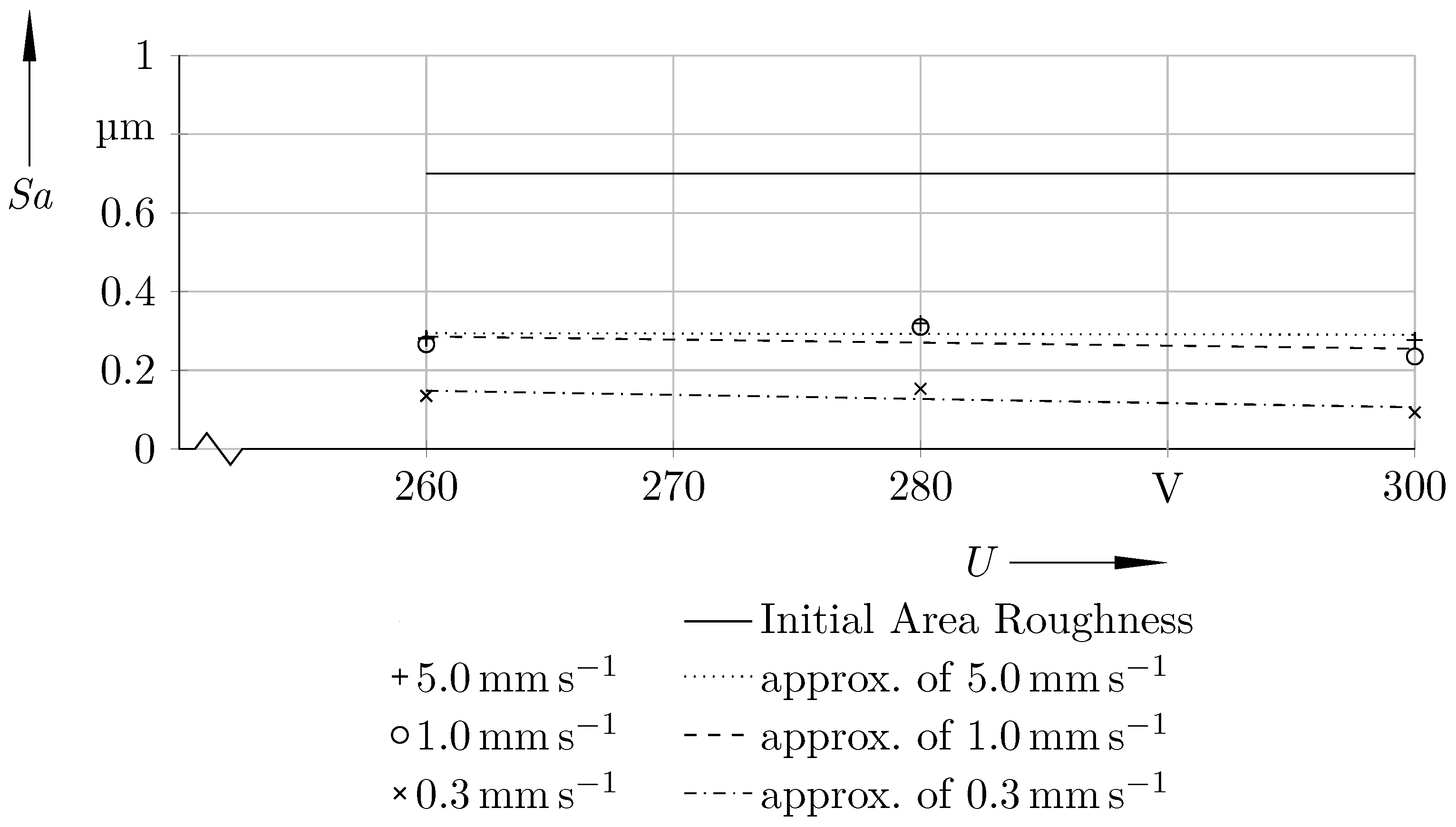
In this section the results of the first measurements are presented and discussed. The intention is to show that the process of electrolytic plasma polishing of outer surfaces can be transferred to internal pipe surfaces. Preliminary investigations were performed to assess the impact of the velocity of the polishing head to the average area roughness Sa. A 30 mm wide area in the tube was plasma polished. The polishing head went through the tube 10 times with a polishing head gap of 1 mm and a electrolyte volume flow rate of 5 L/min. For each applied potential difference, three surface roughnesses Sa were determined for two experiments. These six measured values Sa have been averaged. The average area roughness Sa was analyses for different velocities of the polishing head. Values for the velocity v in a range between 0.3 and 5.0 mm s−1 were investigated and evaluated (Table 1).
Figure 7 shows the average area roughness Sa in µm over the respective applied polishing potential difference U for each velocity v.
The results show that lower velocities deliver better average area roughness Sa values. This is because the plasma has more time to remove material from the surface. Furthermore it can be seen that the applied potential difference at constant velocities has no significant influence on the average surface roughness Sa. Additionally, the area roughness at 5 mm s−1 has a larger standard deviation than lower velocities. This shows that process-related plasma polishing takes some time to remove the peaks of the surfaces. This is not possible at velocities greater than 1 mm s−1. The best average area roughness of 0.093 µm was achieved at a polishing rate of 0.3 mm s−1 and a applied potential difference of 300 V.
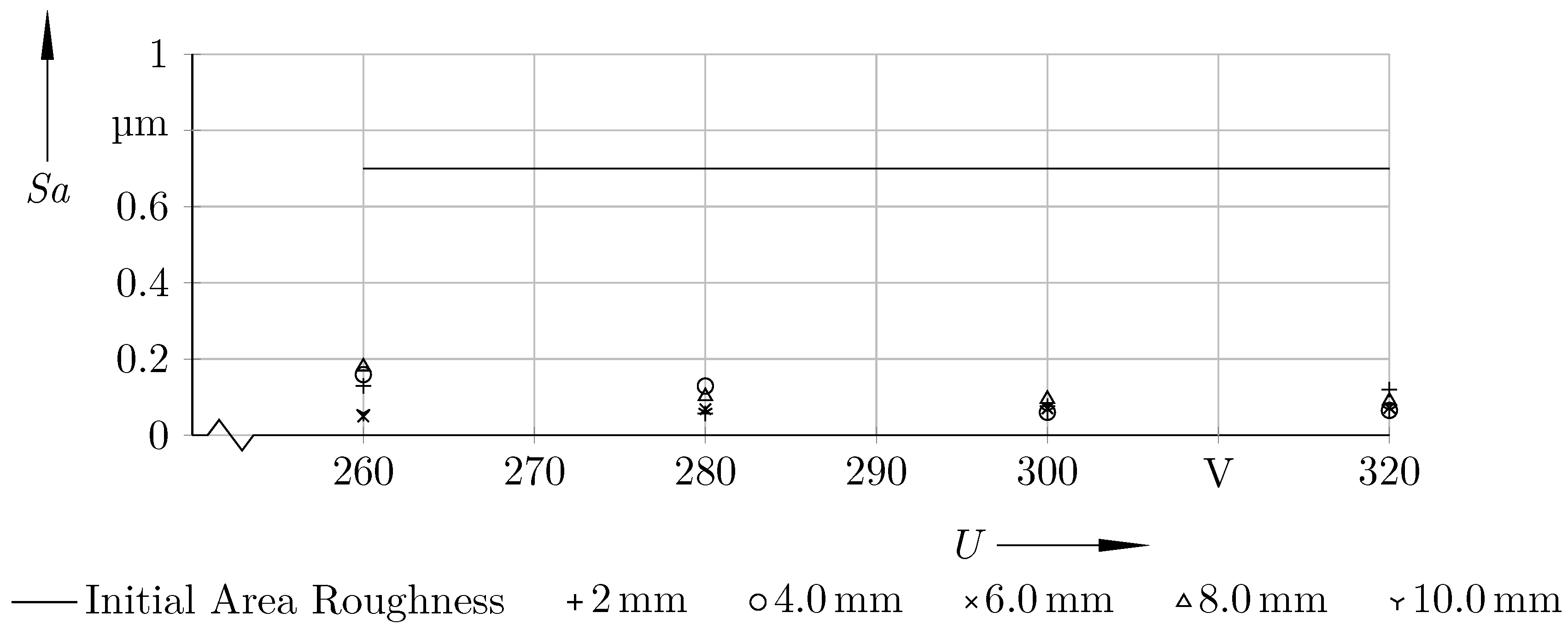
The average area roughness Sa in µm for different applied potential differences U and polishing head gaps are presented in Table 2. A 30 mm wide area in the tube was plasma polished. The polishing head went through the tube 10 times with a flow rate of 51 min−1. The applied potential difference is changed from 260 to 320 V in 20 V steps, the adjustable polishing head gap is changed from 2 to 10 mm in 2 mm steps and due to the low standard deviations the traversing speed of the polishing head was 1 mm s−1. All measured values with the corresponding standard deviations are presented in Table 2. The average area roughness Sa has been calculated from three area roughnesses. The experiment was repeated and three surface roughnesses Sa were determined, after each experiment all six roughnesses were averaged. The current was measured every second. All current values were averaged.
Figure 8 is a graphical representation of measured average area surface roughness values Sa.
In Figure 8 it can clearly be seen that depending on the adjustable polishing head gap and the potential difference the average area roughness Sa lies within the range of 0.049–0.180 µm. Furthermore the average area roughness decreases with increasing potential difference. It indicates that the process is more stable with increasing voltage. Additionally, it can be seen that with increasing potential difference the width of the adjustable polishing head gap has no significant influence on the average surface roughness. Sa achieves a range between 0.065 µm and 0.090 µm.
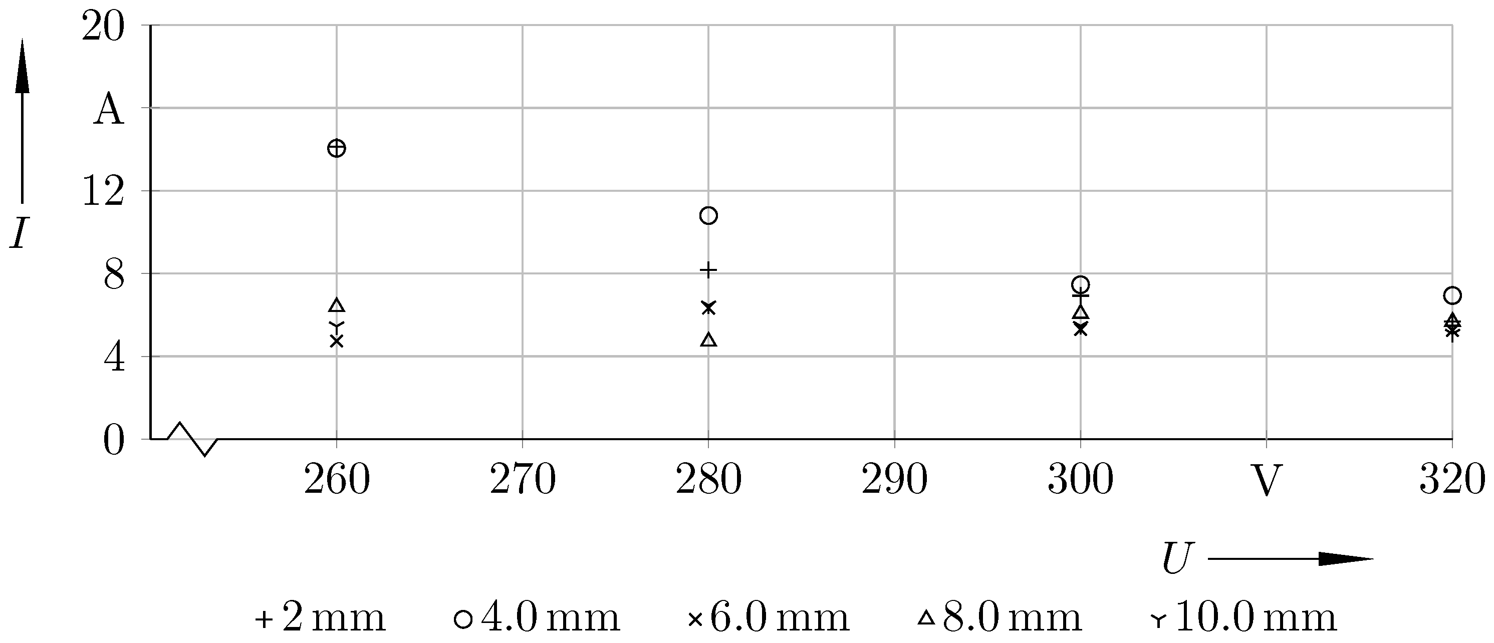
Figure 9 shows the corresponding average polishing currents in A depending on the respective applied polishing potential difference U as a function of the adjustable polishing head gap. The range of the average polishing current I extends from 4.7 to 14.1 A (Figure 9) and this is an indicator that more area (23.5–70.5 cm2 with JEPP of approximately 0.2 A cm−2) is being polished with increasing average current. Furthermore, the trend in average current corresponds with the average area roughness of Figure 8. The variation of the average current decreases with increasing voltage and there is a tendency to reach a stable average current value range of 5 A to 7 A.
Figure 10 shows the top view of an unpolished and a polished tube inner surface. It can clearly be seen that a reduction in the surface roughness Sa has occurred. The unpolished surface has a surface roughness Sa of approximately 0.678 µm. However, in the plasma-polished surface, Sa-values of 0.029 µm were obtained. Furthermore all plasma polished workpieces have a high gloss in contrast to unpolished areas.
5. Conclusions
In this paper, electrical and plasma polishing processes were presented. Furthermore, a method for plasma polishing of media-carrying inner pipe surfaces and the first experimental results were presented. It could be shown that the process of plasma polishing of exterior surfaces could be transferred to tube inner surfaces. It can be seen that a stable process is accompanied by an increasing potential difference and that the average surface roughness Sa reaches a range from 0.065 to 0.090 µm. At the same time, it was shown that with increasing potential difference, the average surface roughness becomes independent of the width of the adjustable polishing head gap. In the future, appropriate process parameters or variations should be found in order to further improve the surface roughness Sa of internal surfaces of pipes and to ensure cost effectiveness. Furthermore, measurements with the competing process (electro polishing) should be conducted in order to compare the achievable surface roughnesses.
Acknowledgments
Special thanks to Tobias Weise from plasotec GmbH for support relating to the electrolytic plasma polishing process.
Author Contributions
Matthias Cornelsen and Carolin Deutsch conceived and designed the experiments; performed the experiments; contributed reagents/materials/analysis tools; Matthias Cornelsen and Hermann Seitz analysed the data and wrote the paper.
Conflicts of Interest
The authors declare no conflict of interest.
References
- Van Gils, S.; Le Pen, C.; Hubin, A.; Terryn, H.; Stijns, E. Electropolishing of copper in H3PO4: Ex situ and in situ optical characterization. J. Electrochem. Soc. 2007, 154, C175–C180. [Google Scholar] [CrossRef]
- Duradji, V.; Kaputkin, D. Metal Surface Treatment in Electrolyte Plasma during Anodic Process. J. Electrochem. Soc. 2016, 163, E43–E48. [Google Scholar] [CrossRef]
- Buhlert, M. Elektropolieren und Elektrostrukturieren von Edelstahl, Messing und Aluminium: Untersuchung des transpassiven Abtragprozesses Einschließlich unerwünschter Nebeneffekte; VDI-Verlag: Düsseldorf, Germany, 2000. [Google Scholar]
- Buhlert, M. Elektropolieren: Elektrolytisches Glänzen, Glätten und Entgraten von Edelstahl, Stahl, Messing, Kupfer, Aluminium und Titan; mit 4 Tabellen; Leuze: Bad Saulgau, Germany, 2009. [Google Scholar]
- Podhorský, S.; Malík, A. The Possibilities of Plasma Polishing of the Steel DIN 1.0570 in Electrolyte. In Proceedings of the 19th Conference Metal 2010, Zlín Region, Czech Republic, 18–20 May 2010. [Google Scholar]
- Kuhn, A. The electropolishing of titanium and its alloys. Met. Finish. 2004, 102, 80–86. [Google Scholar] [CrossRef]
- Böttger-Hiller, F.; Nestler, K.; Zeidler, H.; Glowa, G.; Lampke, T. Plasma electrolytic polishing of metalized carbon fibers. Aims Mater. Sci. 2016, 3, 260–269. [Google Scholar] [CrossRef]
- Zeidler, H.; Böttger-Hiller, F.; Edelmann, J.; Schubert, A. Surface finish machining of medical parts using Plasma electrolytic Polishing. Procedia CIRP 2016, 49, 83–87. [Google Scholar] [CrossRef]
- Zeidler, H.; Nestler, K.; Böttger-Hiller, F.; Schubert, A.; Previtali, B.; Demir, A. Finishing of laser-machined coronary stents by plasma electrolytic polishing. In Proceedings of the 16th International Conference of the European Society for Precision Engineering and Nanotechnology, EUSPEN, Nottingham, UK, 30 May–3 June 2016. [Google Scholar]
- Weingarten, C.; Schmickler, A.; Willenborg, E.; Wissenbach, K.; Poprawe, R. Laser polishing and laser shape correction of optical glass. J. Laser Appl. 2017, 29, 011702. [Google Scholar] [CrossRef]
- Ostholt, R.; Willenborg, E.; Wissenbach, K. Laser polishing of freeform surfaces. In Proceedings of the 5th International WLT-Conference on Lasers in Manufacturing, Munich, Germany, 15–18 June 2009; pp. 397–402. [Google Scholar]
- Gora, W.; Tian, Y.; Cabo, A.; Ardron, M.; Maier, R.; Prangnell, P.; Weston, N.; Hand, D. Enhancing surface finish of additively manufactured titanium and cobalt chrome elements using laser based finishing. Phys. Procedia 2016, 83, 258–263. [Google Scholar] [CrossRef]
- Bordatchev, E.; Hafiz, A.; Tutunea-Fatan, O. Performance of laser polishing in finishing of metallic surfaces. Int. J. Adv. Manuf. Technol. 2014, 73, 35–52. [Google Scholar] [CrossRef]
- Nestler, K.; Böttger-Hiller, F.; Adamitzki, W.; Glowa, G.; Zeidler, H.; Schubert, A. Plasma Electrolytic Polishing—An Overview of Applied Technologies and Current Challenges to Extend the Polishable Material Range. Procedia CIRP 2016, 42, 503–507. [Google Scholar] [CrossRef]
- Landolt, D. Fundamental Aspects of Electropolishing. Electrochim. Acta 1987, 32, 1–11. [Google Scholar] [CrossRef]
- Kißling, S. Chemische und Elektrochemische Methoden zur Oberflächenbearbeitung von Galvanogeformten Nickel-Mikrostrukturen; KIT Scientific Publishing: Karlsruhe, Germany, 2010; Volume 6. [Google Scholar]
- Parfenov, E.; Farrakhov, R.; Mukaeva, V.; Gusarov, A.; Nevyantseva, R.; Yerokhin, A. Electric field effect on surface layer removal during electrolytic plasma polishing. Surf. Coat. Technol. 2016, 307, 1329–1340. [Google Scholar] [CrossRef]
- Parfenov, E.; Yerokhin, A.; Nevyantseva, R.; Gorbatkov, M.; Liang, C.J.; Matthews, A. Towards smart electrolytic plasma technologies: An overview of methodological approaches to process modelling. Surf. Coat. Technol. 2015, 269, 2–22. [Google Scholar] [CrossRef]
- Yerokhin, A.; Nie, X.; Leyland, A.; Matthews, A.; Dowey, S. Plasma electrolysis for surface engineering. Surf. Coat. Technol. 1999, 122, 73–93. [Google Scholar] [CrossRef]
- Nestler, K.; Adamitzki, W.; Glowa, G.; Zeidler, H. Plasma Electrolytic Surface Treatment of Copper and Copper Alloys [Plasma-elektrolytische Oberflächenbehandlung von Kupfer und Kupferlegierungen]. Metall 2014, 68, 73–93. [Google Scholar]
- DIN 10528:2009-06. Lebensmittelhygiene–Anleitung für die Auswahl von Werkstoffen für den Kontakt mit Lebensmitteln–Allgemeine Grundsätze; Deutsches Institut für Normung e.V.: Berlin, Germany, 2009. [Google Scholar]
- ISO 4287:1997-04. Geometrical Product Specifications (GPS)–Surface Texture: Profile Method—Terms, Definitions and Surface Texture Parameters; International Organization for Standardization (ISO): Geneva, Switzerland, 1997. [Google Scholar]
- ISO 12085:1996-08. Geometrical Product Specifications (GPS)–Surface Texture: Profile Method—Motif Parameters; International Organization for Standardization (ISO): Geneva, Switzerland, 1996. [Google Scholar]
- Wang, J.; Suo, L.; Guan, L.; Fu, Y. Optimization of Processing Parameters for Electrolysis and Plasma Polishing. Appl. Mech. Mater. 2012, 217–219, 1368–1371. [Google Scholar] [CrossRef]
- Vaňa, D.; Podhorský, S.; Hurajt, M.; Hanzen, V. Surface Properties of the Stainless Steel X10 CrNi 18/10 after Application of Plasma Polishing in Electrolyte. Int. J. Mod. Eng. Res. 2013, 3, 788–792. [Google Scholar]
- Vaňa, D.; Podhorský, S.; Suba, R.; Hurajt, M. The Change of Surface Properties on tested Smooth Stainless Steel Surfaces after Plasma Polishing. Int. J. Eng. Sci. Invent. 2013, 2, 2319–6734. [Google Scholar]
- Wang, J.; Suo, L.; Guan, L.; Fu, Y. Analytical Study on Mechanism of Electrolysis and Plasma Polishing. Adv. Mater. Res. 2012, 472–475, 350–353. [Google Scholar] [CrossRef]
Figure 1.
Schematic design for electrolytic polishing method ((1) DC voltage source, (2) aqueous electrolyte, (3) workpiece (anode), (4) active medium, (5) basin (cathode)) [24].
Figure 1.
Schematic design for electrolytic polishing method ((1) DC voltage source, (2) aqueous electrolyte, (3) workpiece (anode), (4) active medium, (5) basin (cathode)) [24].
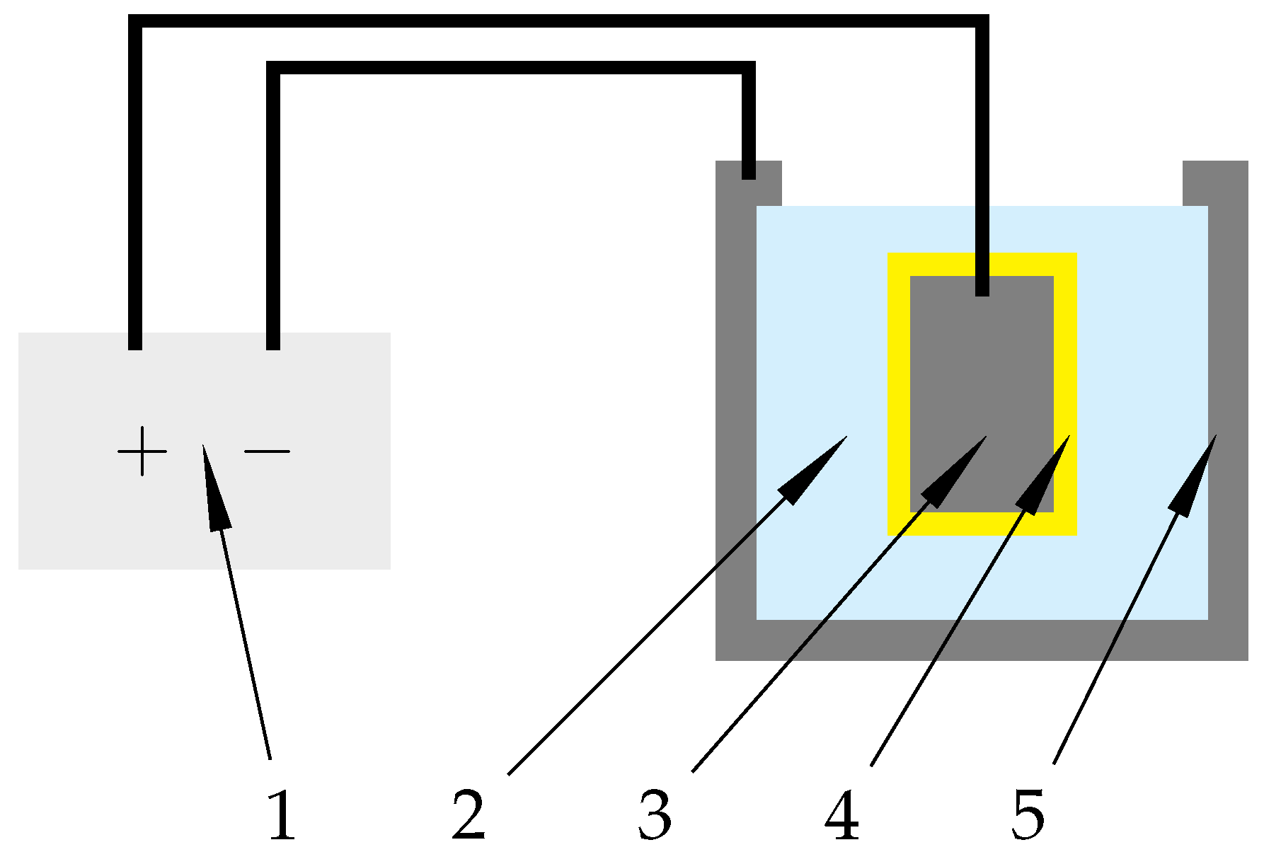
Figure 2.
Schematic illustration of the profile of the surface to be processed during electro polishing. (Idealized electrolyte and anodic film) [25].
Figure 2.
Schematic illustration of the profile of the surface to be processed during electro polishing. (Idealized electrolyte and anodic film) [25].
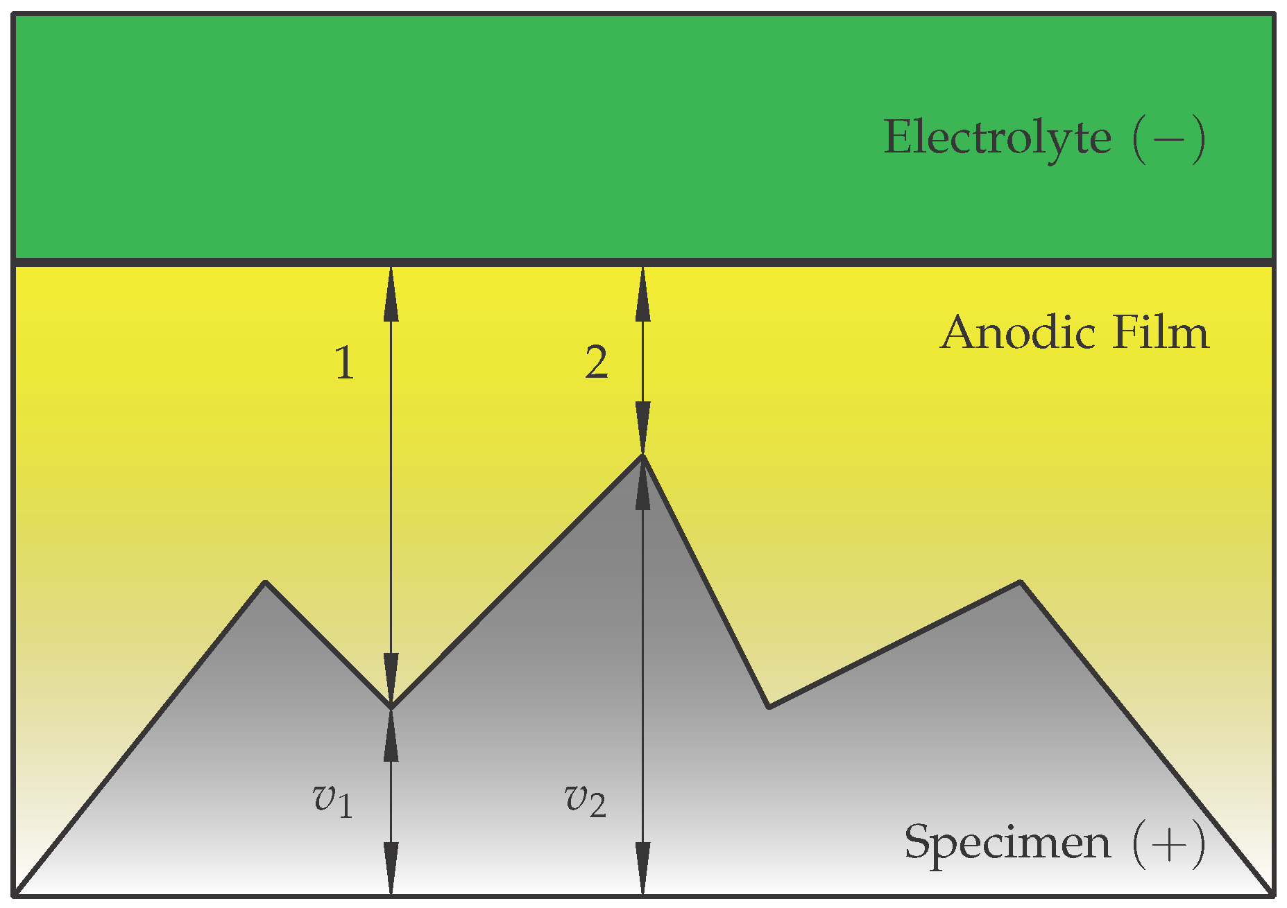
Figure 3.
Schematic representation of the profile of the surface to be processed during the electrolytic plasma polishing (idealized electrolytes and ionized water gas film) [25].
Figure 3.
Schematic representation of the profile of the surface to be processed during the electrolytic plasma polishing (idealized electrolytes and ionized water gas film) [25].
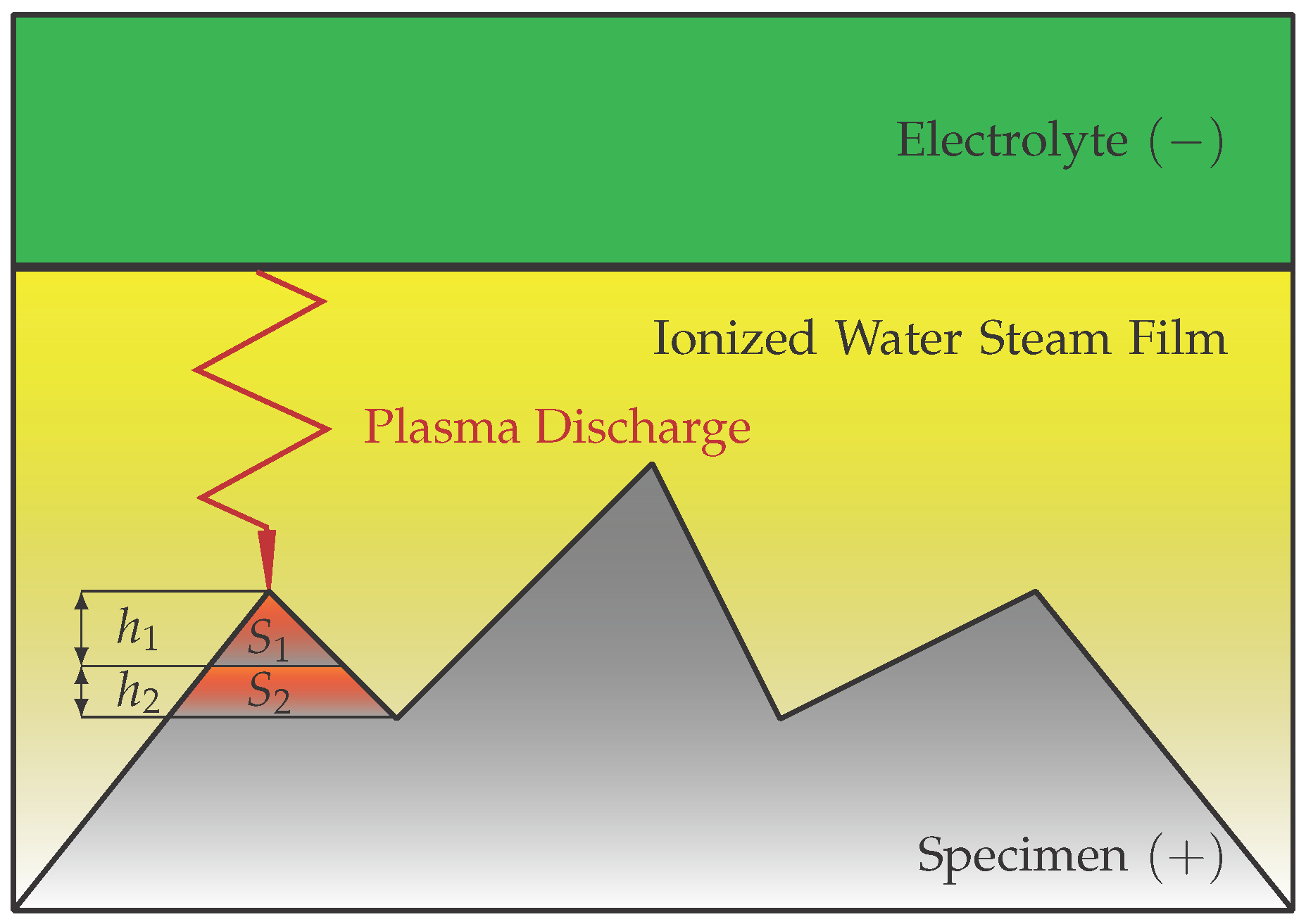
Figure 4.
Schematic of the formation of a plasma discharge according to streamer theory [27]. (a) Electrolytic reaction between the electrolyte (1) and the metal part (5). Electrons (4) and ions (3) forming a continuous layer and moving to the specimen. The electrons are much faster than the ions. (b) The electrons form an avalanche head (7) while the ions remain in the back nearly stationary as an avalanche tail. Secondary electrons (6) are formed resulting from the photoionization (2). (c) Those electrons are accelerated and form secondary avalanches. (d) Due to the field distortion, secondary avalanches are attracted by the head of the primary avalanche. As a result of the sum of the avalanches, the formation of an initially weak conductive channel (streamer (8)) begins. (e) The streamer generates a plasma channel. (f) Under the influence of the pinch effect the plasma channel (9) becomes denser and hotter. The result of the opposing processes of gas expansion (10) and compression is an explosion.
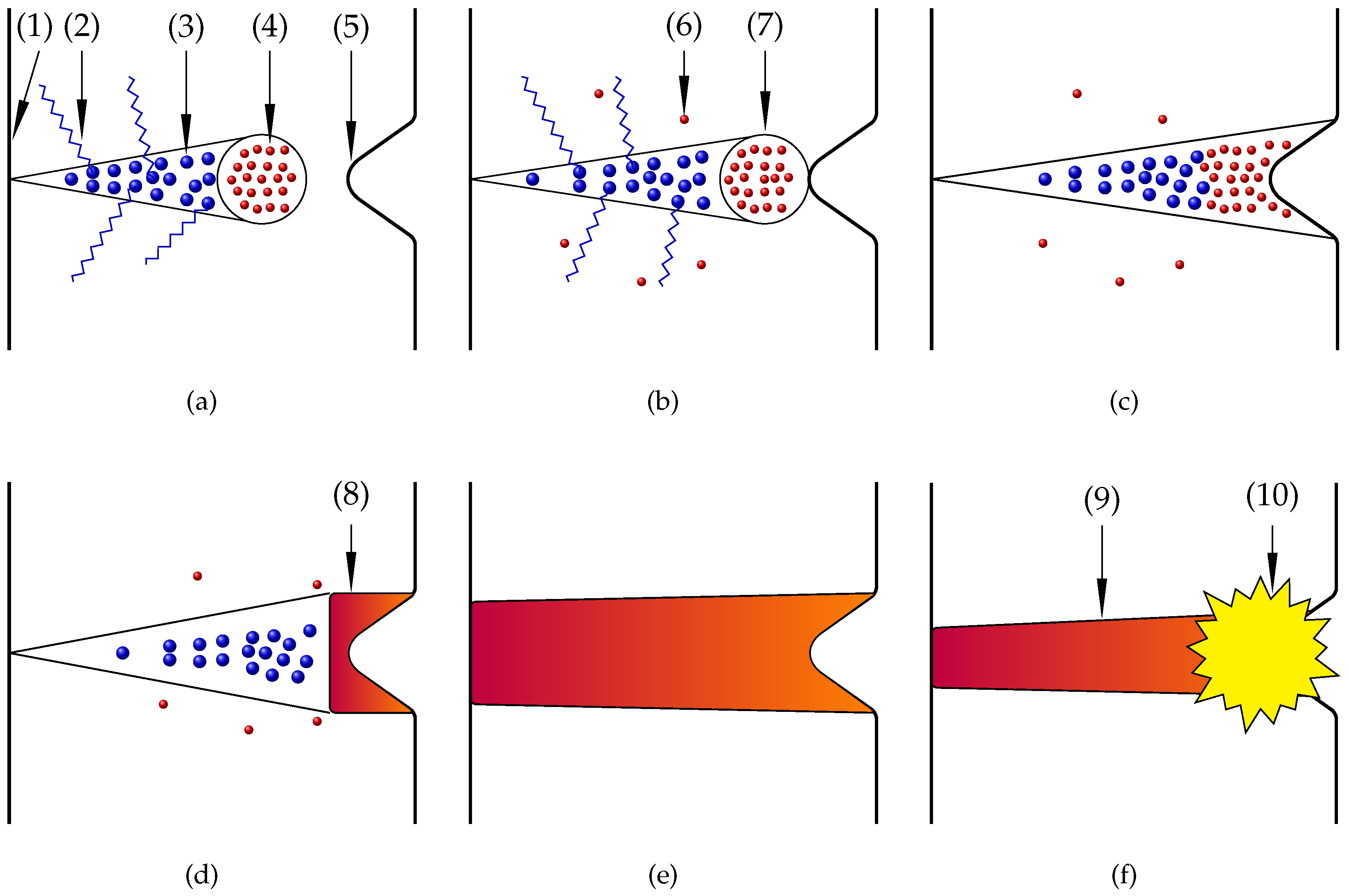
Figure 5.
Schematic design of a plasma polishing system for internal pipe surfaces: (1) DC power supply, (2) polishing head (cathode), (3) tube clamping, (4) tube (anode), (5) spindle drive with vertical axis, (6) basin, (7) electrolyte.
Figure 5.
Schematic design of a plasma polishing system for internal pipe surfaces: (1) DC power supply, (2) polishing head (cathode), (3) tube clamping, (4) tube (anode), (5) spindle drive with vertical axis, (6) basin, (7) electrolyte.
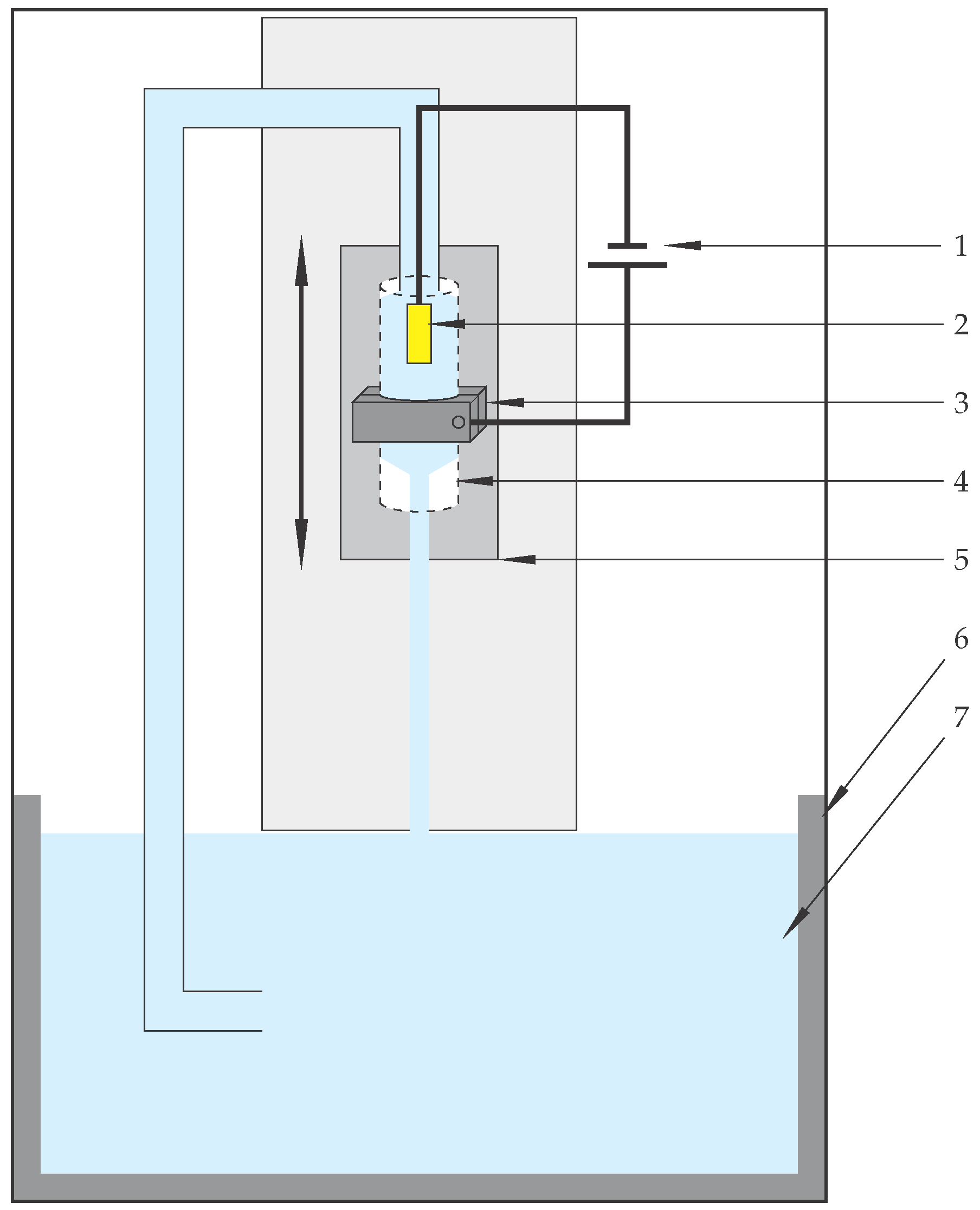
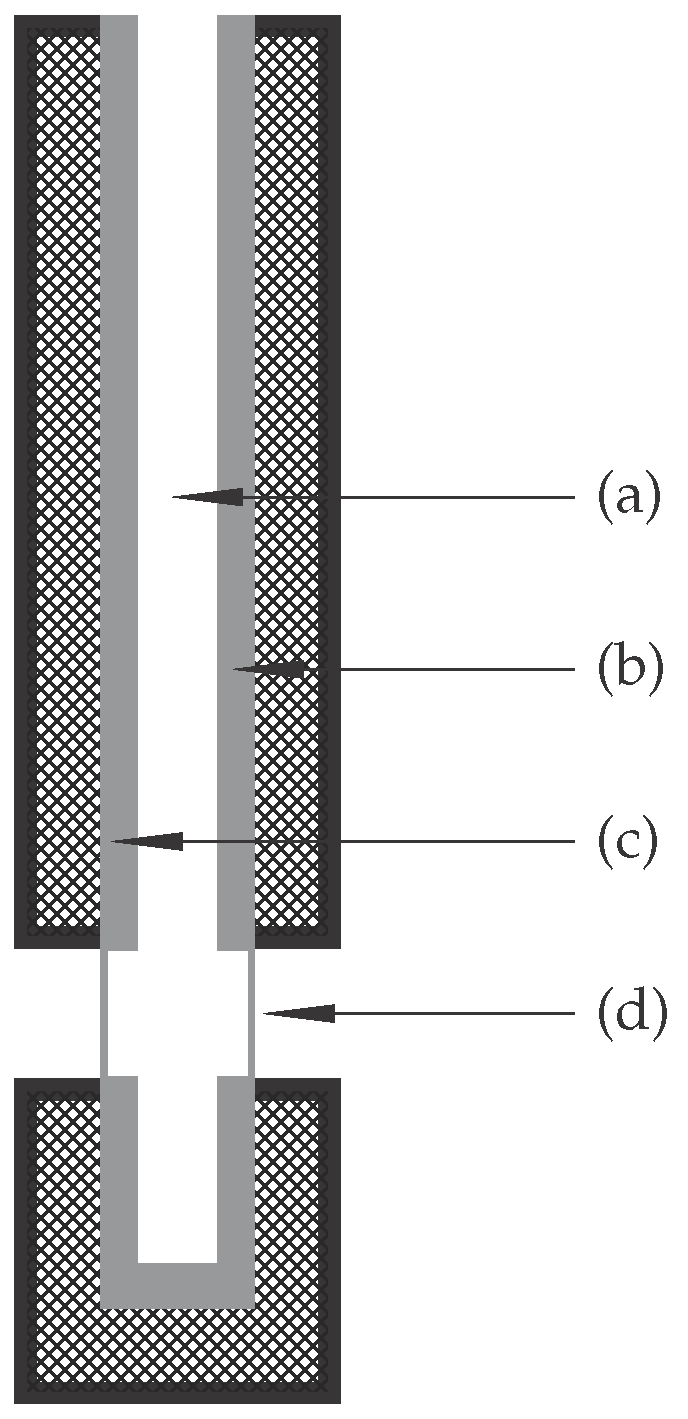
Figure 6.
Schematic design of the polishing head (Figure 5 (2)): (a) fluid (b) metal core (cathode) (c) isolator (d) adjustable polishing head gap.
Figure 6.
Schematic design of the polishing head (Figure 5 (2)): (a) fluid (b) metal core (cathode) (c) isolator (d) adjustable polishing head gap.

Figure 7.
Average area roughness Sa over applied potential difference U for different velocities v of the polishing head.
Figure 7.
Average area roughness Sa over applied potential difference U for different velocities v of the polishing head.

Figure 8.
Average area surface roughness Sa depending on the applied potential difference U for different widths of the polishing head gap width.
Figure 8.
Average area surface roughness Sa depending on the applied potential difference U for different widths of the polishing head gap width.

Figure 9.
Average polishing current I depending on applied polishing potential difference for different polishing head gap width values.
Figure 9.
Average polishing current I depending on applied polishing potential difference for different polishing head gap width values.

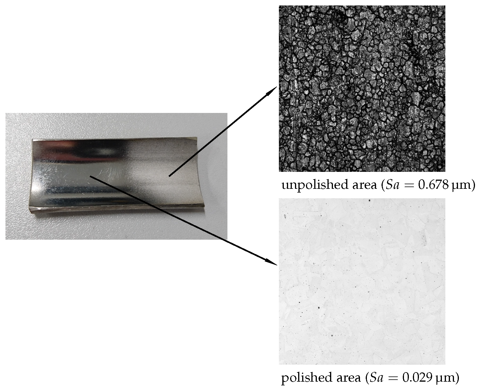
Figure 10.
On the left side a cut tube with a unpolished and polished area can be seen. The polished area is glossy in contrast to the matt unpolished area. On the right, there is a CLSM image of an unpolished (Sa = 0.678 µm) and plasma polished surface (Sa = 0.029 µm). The polishing head went through the tube 10 times with a applied potential difference of 320 V and a velocity of 1 mm s−1. The scan area is 258 µm × 250 µm with a cut-off wavelength of 25 µm.


Table 1.
Average area surface roughness Sa in µm depending on the applied potential difference U in V for different velocities of the polishing head.
Table 1.
Average area surface roughness Sa in µm depending on the applied potential difference U in V for different velocities of the polishing head.
| Velocity of the Adjustable Head Gap in mm s−1 | U = 260 V | U = 280 V | U = 300 V |
|---|---|---|---|
| 5.0 | 0.281 ± 0.067 | 0.319 ± 0.075 | 0.277 ± 0.047 |
| 1.0 | 0.266 ± 0.031 | 0.310 ± 0.010 | 0.235 ± 0.041 |
| 0.3 | 0.135 ± 0.028 | 0.153 ± 0.035 | 0.093 ± 0.029 |
Table 2.
Average area surface roughness Sa in µm and average current I in A depending on the applied potential difference U in V for different polishing head gap values from 2–10 mm and constant velocity of the polishing head of 1 mm s−1.
Table 2.
Average area surface roughness Sa in µm and average current I in A depending on the applied potential difference U in V for different polishing head gap values from 2–10 mm and constant velocity of the polishing head of 1 mm s−1.
| Gap Width in mm | U = 260 V | U = 280 V | U = 300 V | U = 320 V |
|---|---|---|---|---|
| 2 | Sa = 0.129 ± 0.063 | Sa = 0.057 ± 0.006 | Sa = 0.076 ± 0.015 | Sa = 0.120 ± 0.041 |
| 4 | Sa = 0.159 ± 0.087 | Sa = 0.129 ± 0.047 | Sa = 0.060 ± 0.013 | Sa = 0.065 ± 0.002 |
| 6 | Sa = 0.049 ± 0.006 | Sa = 0.068 ± 0.002 | Sa = 0.070 ± 0.001 | Sa = 0.072 ± 0.008 |
| 8 | Sa = 0.180 ± 0.080 | Sa = 0.102 ± 0.003 | Sa = 0.095 ± 0.013 | Sa = 0.090 ± 0.002 |
| 10 | Sa = 0.057 ± 0.006 | Sa = 0.060 ± 0.006 | Sa = 0.063 ± 0.001 | Sa = 0.066 ± 0.005 |
| 2 | I = 14.1 ± 14.1 | I = 8.2 ± 6.2 | I = 6.9 ± 2.9 | I = 5.7 ± 1.4 |
| 4 | I = 14.1 ± 15.7 | I = 10.8 ± 11.0 | I = 7.5 ± 3.0 | I = 6.9 ± 1.9 |
| 6 | I = 4.7 ± 1.2 | I = 6.3 ± 1.9 | I = 5.3 ± 1.3 | I = 5.3 ± 1.1 |
| 8 | I = 6.4 ± 7.2 | I = 4.7 ± 3.7 | I = 6.1 ± 4.0 | I = 5.7 ± 1.6 |
| 10 | I = 5.5 ± 1.4 | I = 6.5 ± 1.4 | I = 5.5 ± 1.0 | I = 5.1 ± 1.2 |
© 2017 by the authors. Licensee MDPI, Basel, Switzerland. This article is an open access article distributed under the terms and conditions of the Creative Commons Attribution (CC BY) license (http://creativecommons.org/licenses/by/4.0/).
Share and Cite
MDPI and ACS Style
Cornelsen, M.; Deutsch, C.; Seitz, H. Electrolytic Plasma Polishing of Pipe Inner Surfaces. Metals 2018, 8, 12. https://doi.org/10.3390/met8010012
AMA Style
Cornelsen M, Deutsch C, Seitz H. Electrolytic Plasma Polishing of Pipe Inner Surfaces. Metals. 2018; 8(1):12. https://doi.org/10.3390/met8010012
Chicago/Turabian StyleCornelsen, Matthias, Carolin Deutsch, and Hermann Seitz. 2018. "Electrolytic Plasma Polishing of Pipe Inner Surfaces" Metals 8, no. 1: 12. https://doi.org/10.3390/met8010012
Note that from the first issue of 2016, this journal uses article numbers instead of page numbers. See further details here.