Microstructure, Micro-Indentation, and Scratch Behavior of Cr Films Prepared on Al alloys by Using Magnetron Sputtering


1
Tianjin Key Laboratory of Materials Laminating Fabrication and Interface Control Technology, Research Institute for Energy Equipment Materials, School of Material Science and Engineering, Hebei University of Technology, Tianjin 300130, China
2
School of Metallurgy, Northeastern University, Shenyang 110819, China
3
College of Materials Science and Engineering, Nanjing Tech University, Nanjing 211816, China
*
Authors to whom correspondence should be addressed.
Metals 2019, 9(12), 1330; https://doi.org/10.3390/met9121330
Submission received: 5 November 2019
/
Revised: 29 November 2019
/
Accepted: 6 December 2019
/
Published: 9 December 2019
Abstract
:In this study, closed-field unbalanced magnetron sputtering (CFUMS) was employed to deposit pure Cr films on soft substrate of 2024 Al alloy. The effects of deposition powers and biases on the microstructures and mechanical performance of Cr films were systematically investigated by using X-ray diffraction (XRD), scanning electron microscope (SEM), micro-indentation and scratch test. Results showed that all the Cr films had a strong (110) preferred orientation and anisotropic surface morphology with columnar structures. The size of Cr particles was in the range of 50–350 nm, increasing with larger target power and higher biases. The hardness of Cr films was between 3.3 and 4.8 GPa, which was much higher than the Al alloy substrate (1.44 GPa). The Young’s modulus of Cr film could reach a maximum value of 169 GPa at 2.0 kW/70 V. The critical load increased when increasing the power but decreased with higher bias, achieving a maximum value of 53.83 N at 2.0 kW/10 V. The adhesive failure mechanism of Cr film was mainly attributed to the plastic deformation of softer Al substrate.
1. Introduction
As an important engineering material, Cr has a strong passivation effect in the atmosphere and can maintain metallic shining for a long time. It has relatively high hardness, good electrical resistivity, and good chemical stability by the formation of dense chromia layers [1]. Thus, Cr is commonly employed as protective coating or film for metal parts at aggressive friction condition, corrosion, and high-temperature oxidation [2]. Generally, Cr coatings are fabricated by electroplating [3,4] and physical vapor deposition (PVD) [2,5,6,7,8]. However, the traditional Cr plating process uses a highly toxic CrO3 electrolyte, and a large amount of waste liquid discharges cause serious pollution to the environment. In recent years, many countries have introduced laws or strict restrictions on electroplated hard chromium. Therefore, it is a trend to develop environmentally friendly and fast depositing methods to produce Cr coatings.
Magnetron sputtering, as one of PVD technique, is a well-established and very effective method of film deposition. It could provide uniform structure, controllable film thickness, and good film–substrate bond. Moreover, the target materials come from a wide variety of materials including almost all metals, alloys, and ceramics. Several studies have reported the feasibility to deposit Cr films by magnetron sputtering [5,6,7,8]. Compared with CrO3 electrolyte, metal Cr target could be less hazardous. The deposition parameters to control the quality of Cr film would be the main concern.
Paturaud [9] employed DC magnetron sputtering (DCMS) to prepare Cr films, with the hardness varying from 4 to 12.3 GPa. By adjusting deposition conditions such as target power and substrate bias, the Cr film could be harder than electroplating Cr coating. Generally, Cr film showed a preferred (110) crystal orientation, but under very low DC power condition, Cr film could be an amorphous structure and the thickness would be rather thin (<300 nm thickness) [6]. Chiang [10] used plasma-enhanced magnetron sputtering (PEMS) technique to deposit Cr film and found that higher level of ion bombardment led to denser and continuous film. The preferred orientation of film also transferred from Cr (110) to Cr (200) due to increased atoms mobility. Ferreira [11,12] pointed out that deep oscillation magnetron sputtering (DOMS) could obtain much denser Cr film than DCMS deposition. By increasing peak power, the hardness of Cr film could reach 17 GPa and the Young’s modulus always has a close value to bulk material (279 GPa). DOMS provided additional control of the flux of impinging species, thus minimize the effects of geometrical asymmetries.
Generally, the high self-ion bombardment or re-sputtering effect in PVD method would reduce deposition rate and change the film microstructure. For instance, intense ion bombardment was reported to induce preferred (200) orientation of Cr films deposited by using arc ion-plating [2]. As reported by Sidelev [7], hot target magnetron sputtering was taken to decrease the re-sputtering effect during Cr film growing and reduce the loss of deposition rate. The applied bias and high deposition rate led to the formation of irregular microstructure of Cr films. Recently, Daure [5] found that Cr film deposited by using unbalanced magnetron sputtering (UMS) and electron beam PVD (EBPVD) showed obvious preferred orientations and close hardness (~5 GPa), but UMS Cr film showed similar galling resistance with conventional hard chromium electroplating (EPHC), which was much better than EBPVD Cr. Daure pointed out UMS would have potential to replace EPHC in some tribological applications.
However, the above introduction indicates that various PVD techniques result in different film microstructures. Moreover, the processing conditions such as bias and power play an important role in controlling the film quality, and thus need to be further explored. With the aim to obtain more comprehensive information about PVD depositing Cr films, in the present study, closed-field unbalanced magnetron sputtering (CFUMS) was employed to deposit pure Cr films on Al alloy substrates. The key parameters of substrate bias and target power were selected to investigate the effects on microstructures and mechanical performance of Cr film. The failure mechanism of Cr films during scratching was also discussed.
2. Materials and Methods
A total of 2024 Al alloy disks with 20 mm diameter and 4 mm thickness were used as substrates. These samples were grounded with silicon carbide paper, polished with diamond abrasive paste, and ultrasonically oscillated in acetone.
An unbalanced magnetron sputtering ion-plating system (UDP-450, Teer Coatings Ltd., Droitwich, UK) was used for deposition. The Cr target (purity, 99.999%) was used for depositing. The Al disks were placed on a rotatable work stage (5 r/min) in the center of the furnace chamber. The distance of target-substrate was 80 mm. The surface of each Al substrate was parallel to the target plane to ensure the homogenous deposition. Firstly, the base pressure of the vacuum chamber was evacuated to 3 × 10⁻³ Pa, then filled with Ar at the flux of 16 sccm. Before deposition, Al substrates were sputter cleaned for 30 min at a bias of 400 V. Then, the power of the Cr target was turned on and the substrate bias set to grow Cr films. As displayed in Table 1, in this study, different Cr films (denoted as DC1-DC7) were deposited by altering the Cr target power and substrate bias.
The phase structure of Cr films was analyzed by using Bruker D8-Advance X-ray diffraction (XRD) system with Cu-Kα radiation (λ = 1.5418 Å). Grazing incidence angle was 1.0° and scan range was from 20° to 90° with a 0.06° step. The observation of surface, cross-sectional, and fracture morphologies were conducted by using scanning electron microscopy (SEM, JSM-7100F, JEOL Ltd., Tokyo, Japan). In order to assess the coating fracture resistance and adhesive strength, scratch tests were conducted on micro-scratch test (WS-2005, Lanzhou institute of chemical physics, Lanzhou, China) with a diamond tip. The maximum load, loading rate and scratch distance were set at 80 N, 60 N/min, and 3 mm, respectively. The mechanical properties of Cr films were evaluated by using a dynamic ultra-micro hardness tester (DUH-211S, SHIMADZU, Kyoto, Japan). The test force and loading speed were 5 mN and 1 mN/s, respectively. The load–displacement curves were obtained to calculate indentation hardness and Young’s modulus.
3. Results and Discussions
3.1. Phase Structures
Figure 1 shows the XRD patterns of Cr films deposited at different biases and powers. All the Cr films show a crystalline structure with strong preferred orientation of (110) plane (PDF card, 85-1336) [13]. Weak (211) peaks are also visible at some conditions (Figure 1b). The presence of Al peaks reveals that the X-ray penetrates through the two Cr films because of the low thickness deposited at low target power (<0.8 kW). However, it has no effect on the peak patterns of Cr film. Similar (110) texture is also reported in Cr films produced by other DC magnetron sputtering techniques [11]. This is because the (110) plane in the bcc Cr structure has the lowest surface energy [14]. As seen from Figure 1b, the peak intensity ratio of Cr (211)/(110) decreases, indicating that the Cr (110) preferential growth is slightly reduced.
3.2. Top Surface Morphologies
Figure 2 shows the top surface morphologies of Cr films deposited at different target powers. The images at the left side and right side in Figure 2 were taken from low and high magnifications, respectively. All the Cr films are made of faceted three-sided pyramided-like columns and the surface morphologies look rather anisotropic. The internal voids are apparent between the adjacent columns. The corresponding column size is described in Figure 3. At low power (0.2 kW), the column is rather fine (Figure 2a,b) with a size of 50 ± 10 nm. With increasing power to 0.8 kW, the column size grows larger, with an average size of 218 ± 31 nm. Ridges are also observed on the pyramidal side of columns, which might result from the conjugate growth of adjacent columns. When further increasing power to 1.4 kW, abnormally large columns occur with the size of ~420 nm. The other small columns have a close size with that at 0.8 kW.
The top-view micrographs of Cr film deposited with different bias at 2.0 kW are described in Figure 4. All the Cr films also show three-sided pyramided-like shape, similar with Cr films deposited at different powers in Figure 2. The corresponding column size is displayed in Figure 5. At low bias (<70 V), the Cr columns have homogenous size, 178 ± 31 nm and 230 ± 20 nm for Cr films at 10 V and 30 V, respectively. It is close to the size of Cr film deposited at 0.8 kW/70 V condition. However, with further increasing bias (>70 V), irregular growth becomes obvious and large columns are distinct on the surface. The average size of Cr columns at 70 V and 110 V are 290 ± 76 nm and 353 ± 75 nm, respectively. Actually, the size of small Cr columns at 110 V (~300 nm) is larger than that at 70 V (~230 nm). According to the results in Figure 2 and Figure 4, it can be inferred that larger target power and higher bias contribute to the increased size of Cr columns and abnormal growth.
3.3. Cross-Sectional and Fracture Morphologies
The cross-sectional and fracture morphologies of Cr films deposited at different powers are given in the left and right side of Figure 6, respectively. Clearly, all Cr films bond well with Al alloy substrate and have a columnar characteristic with elongated columns extending from the substrate to the top surface. This is the reason for the valleys of voids as observed in Figure 2 and Figure 4. According to previous studies [12,14], this columnar microstructure is attributed to the low mobility of the Cr atoms and shadowing effect. Actually, this is a common feature in magnetron sputtering films due to the primary non-local growing mechanism [15]. As the target power increases, the thickness of Cr films increases, i.e., 1.3 μm (0.2 kW), 2.8 μm (0.8 kW), and 4.9 μm (1.4 kW). The Cr column width is correlated to the measured Cr column size from top surface images. As seen from Figure 6b,d,f, the column becomes wider as the power increases.
Figure 7 gives the cross-sectional (left side) and fracture morphologies (right side) of Cr films deposited at different biases. As seen from the backscattered electron (BSE ) images on the left side, distinct fibrous structure like elongated grains can be observed from Al substrate on the top surface. The black lines in Figure 7a,c,e,g are identified as inter-column voids, which are related to the valleys on the top surface (Figure 4). The columnar morphologies are clearly described in the fracture images. Note that the Cr columns at lower bias (<70 V) have a finer width than that at higher bias (>70 V). In addition, the latter leads to more tightly packed microstructure. All Cr films at different biases have flat interfaces with substrate and the thickness of Cr films is 5.8 μm (10 V), 5.5 μm (30 V), 5.1 μm (70 V), and 5.0 μm (110 V), respectively. The increasing bias results in a slight decrease of film thickness, which might be due to the re-sputtering of Cr atoms. However, higher substrate bias is beneficial to form more compact films [11].
Based on the above analysis, all the deposited Cr films have a strong (110) preferential orientation and show anisotropic surface morphologies with faceted pyramidal shapes. The Cr grains grow like columns with a network of inter-connected voids between the adjacent columns. As reported in [11,12], these microstructures are primarily determined by shadowing effect. Even increasing the bias cannot eliminate this effect [16]. The preferentially sputtering etching of other crystal planes of Cr is responsible for the strong orientation of (110) plane [17]. The relatively high power and bias led to form dense Cr films because the atom mobility on film surface increases under these conditions. However, it could induce abnormal growth to form irregular microstructure of Cr films. Ferria [11] employed DOMS process to overcome the shadowing effect to deposit more uniform films at the cost of deposition efficiency. Thus, DC magnetron sputtering is still a widely-spread technique.
3.4. Micro-Indentation Behavior
Figure 8 demonstrates the load-depth curves of Cr films and 2024 Al alloy substrate. Table 2 summarizes hardness (H), elastic modulus (E), and plastic properties of Cr films calculated from these load-unload curves. The hardness of Cr films deposited at different biases (DC1, DC2, DC3, and DC4) is 3.81, 3.60, 4.56, and 4.87 GPa, respectively. As for Cr films deposited at different powers, the hardness is 3.31 (DC5), 4.19 (DC6) and 4.33 GPa (DC7), respectively. Thus, the hardness of 2024 Al alloy substrate (1.44 GPa) is enhanced by surface Cr films. It is clear that higher power and larger bias contribute to the hardness improving of Cr films. It is in accordance with previous reports that substrate biasing often leads to improving film hardness [18,19]. However, the film hardness is lower than that of electroplated Cr coating (~10 GPa) since the deposited films usually have pores or voids.
As seen from Table 2, the Young’s modulus of Cr films increase from 81.5 GPa (DC5) to 164 GPa (DC7) when increasing the target power. The modulus of Cr films deposited at 10 V and 30 V has a close value of ~130 GPa. As the substrate bias increases to 70 V, the modulus of Cr films is improved (167 GPa). The further increase of bias has no obvious change of modulus since the Cr film deposited at 110 V and 70 V has similar microstructure. However, the modulus of present Cr films is significantly lower than the bulk Cr (279 GPa), which is due to the large levels of porosity. It is in agreement with other reports on magnetron deposited films [6,7].
Generally, the tribological property of coatings is not only determined by hardness but also on the reduced Young’s modulus. Thus, elastic strain to failure, which is related to H/E ratio, is more suitable to evaluate the wear resistance [20,21]. As seen from Table 2, the H/E ratio decreases when increasing the target power (DC5–DC7). The H/E ratios have similar values under different bias (DC1–DC4). The relatively large H/E value of Cr films deposited at lower power is probably because of the smaller crystal size (Figure 4). H3/E2 ratio can be used to predict the plastic deformation resistance of coatings [22,23,24]. Larger H3/E2 value indicates better resistance to plastic deformation and higher toughness of coatings. As seen from Table 2, the deposition conditions have a similar impact trend on H3/E2 values with H/E values. The H3/E2 values are much higher than that of 2024 Al alloy substrate, indicating Cr coating can be used to strengthen the surface of Al alloy. As for load-depth curves in Figure 8, the area under the loading curves and the enclosed area by loading and unloading curves are defined as the total deformation work Wt and the plastic deformation work Wp. The plasticity factor ηp (ηp = Wp/Wt) is also used to further assess the plastic properties. The larger values like 0.94 for Al (Table 2) indicate easier for plastic deformation. The trend of ηp values for Cr films is consistent with that of H3/E2 values. Based on the above analysis, the DC4 film has the highest hardness (4.87 GPa) and moderate wear resistance and toughness.
3.5. Scratch Behavior
The adhesion behavior of the Cr films deposited on Al alloy substrates by DC magnetron sputtering at different powers and biases were evaluated by the scratch test. The critical normal load (LC) is used to accurately evaluate the adhesive strength of coating/substrate system, which can be determined from the acoustic emission (AE) signal curves [25,26,27]. The sudden increase in AE signal usually indicates the coating failure related to substrate exposure [28,29]. The normal load at this failure event is defined as LC2, the upper critical load, which can measure the coating “practical adhesion” (adhesion strength). As seen from Figure 9, the Lc2 values of Cr films increases with increasing the target powers, i.e., 6.8 N (0.2 kW), 18.0 N (0.8 kW), and 27.2 N (1.4 kW). However, the Lc2 value decreases as the bias increases, from 53.83 N at 10 V to 44.85 N at 110 V.
As reported by Heinke’s study [29], increasing film thickness could reduce plastic deformation and pile-up of relatively soft substrates, and thus lead to the increase of the critical load. As for thin Cr film/soft Al substrate system, plastic deformation of Al substrate is easy to occur thus resulting in fast adhesive failure under relatively lower loads. Hence, Cr films exhibit better adhesion strength at higher power and lower substrate bias.
Representative SEM micrographs of the scratch track are displayed in Figure 10, which can be used to clearly describe the failure events during scratch test. Figure 10a shows the whole track morphologies of DC3 film from the front cracks to the end exposure. The detail morphologies of typical parts (I, II, III, IV) are given in Figure 10b–i. At the start of sliding (Figure 10b), radial cracks occur on the Cr film and the propagations are nearly along the sliding direction since the load is relatively low. The inter-column separation of Cr films in Figure 10f indicates only cohesive failure of Cr film at this stage (I). As the load increases, dense conformal cracking and scratch groove are observed in the sliding surface (Figure 10c). This reveals ductile failure for Cr films. At the edge of sliding surface (Figure 10g), break-off chips of Cr columns and partial exposure of substrate are visible due to the plastic deformation of Al alloy substrate. Thus, both cohesive and slight adhesive failure occurs in this stage (II).
When the loading further progresses, the Cr columns bend toward the sliding direction (Figure 10d) due to compressive stress along with the radial tensile stresses. This leads to buckling failures of Cr film (Figure 10h), thus resulting in partial peeling on the sliding surface (Figure 10d). Both cohesive and adhesive failure is severe at this stage (III). As the load increases to the upper critical load (LC2), large area of peeling occurs on both the central and edge of the sliding surface (Figure 10e), thus the underlying substrate is exposed. At this stage, the severe plastic deformation of central Al substrate squeezes the edge of the track, leading to large area of direct separating of Cr films from substrate even without bending failure of Cr columns (Figure 10i). Thus, severe adhesive failure of Cr film/Al substrate is a dominant feature at stage IV.
Actually, the scratch resistance of films is mainly related to both the intrinsic properties of films and substrate. At the initial stage (I), the Cr film maintains the column feature but the pyramidal shape is flattened under the compressive stress (Figure 10f). At this time, the film is still firmly adhered to the substrate. Tensile cracking occurs (Figure 11a) because the dynamic contact between the indenter and the film induces tensile stresses behind the indenter [30]. As the load progresses (II, III, IV), cracking in the track center and spallation at the track edge become more and more pronounced. These failure events could be attributed mainly to the softer nature of Al alloy. Due to the progressive load, severe plastic deformation of Al substrate under the Cr film occurs primarily, which is evidenced by the ridges in Figure 11b. This generates simultaneous fragmentation and cracking in the Cr film (Figure 11b).
Meanwhile, the increasing load also leads to column break-off (Figure 11c). The loading indenter gets these fragments and break-off chips pushed down into the substrate (Figure 11d). Then, the Cr films are completely removed from the substrate and the adhesive failure occurs. This failure mechanism often happens in hard coatings/softer substrate systems [31,32]. Hence, according to the above analyses, the consecutive failure events of Cr film under a progressive scratch load can be well described in Figure 12.
4. Conclusions
In this paper, unbalanced magnetron sputtering was employed to deposit Cr films under different target powers and biases. All the Cr films showed a crystalline structure with strong preferred orientation of (110) plane. The bias had no obvious change on this crystallographic orientation. The Cr films grew a columnar structure with well-faceted three-sided pyramidal tops. A network of interconnected voids was developed at the inter-columnar structure due to shadowing effect. As the target power and bias increased, the Cr crystallized, had an abnormal growth, and the columns became wider. Higher substrate bias was also beneficial to form more compact films. The hardness of Cr films was enhanced with increasing power and bias. The Cr film (2.0 kW/70 V) had good comprehensive mechanical properties due to its highest hardness (4.87 GPa) and moderate wear resistance (H/E ratio, 0.0288) and toughness (H3/E2 ratio, 0.004). The adhesion strength of Cr films increased with higher power and lower substrate bias. As the scratch load was lower than Lc2, the failure behavior of Cr films was dominated by cohesive strength. When the load reached Lc2, the failure mechanism was shifted to adhesive failure resulted from the severe plastic deformation of softer Al substrate.
Author Contributions
The work was done in cooperation with the joint efforts of all the authors. Conceptualization and original draft preparation, F.Z. and Y.D.; experiments, Y.D., H.L., J.H., and F.Y.; formal analysis, F.Z. and S.Y.
Funding
This research was funded by National Natural Science Foundation of China (Grant No. 51701062 and 51872073) and Natural Science Foundation of Hebei (Grant No. E2017202066).
Acknowledgments
The authors gratefully acknowledge Mufu Yan and Jun Ma for providing operation of magnetron sputtering.
Conflicts of Interest
The authors declare no conflict of interest.
References
- Mello, C.B.; Mansur, R.A.F.; Santos, N.M. Experimental study of mechanical and tribological behavior of nitrogen ion-implanted chromium thin films. Surf. Coat. Technol. 2017, 312, 123–127. [Google Scholar] [CrossRef]
- Hu, M.; Shen, M.; Liu, Z.; Guo, C.; Li, Q.; Zhu, S. Self-ion bombarded Cr films: Crystallographic orientation and oxidation behaviour. Corros. Sci. 2018, 143, 212–220. [Google Scholar] [CrossRef]
- Bikulčius, G.; Češunienė, A.; Selskienė, A.; Pakštas, V.; Matijošius, T. Dry sliding tribological behavior of Cr coatings electrodeposited in trivalent chromium sulphate baths. Surf. Coat. Technol. 2017, 315, 130–138. [Google Scholar] [CrossRef]
- Liang, A.; Ni, L.; Liu, Q.; Zhang, J. Structure characterization and tribological properties of thick chromium coating electrodeposited from a Cr (III) electrolyte. Surf. Coat. Technol. 2013, 218, 23–29. [Google Scholar] [CrossRef]
- Daure, J.L.; Carrington, M.J.; Shipway, P.H.; McCartney, D.G.; Stewart, D.A. A comparison of the galling wear behaviour of PVD Cr and electroplated hard Cr thin films. Surf. Coat. Technol. 2018, 350, 40–47. [Google Scholar] [CrossRef]
- Wang, S.F.; Lin, H.C.; Bor, H.Y.; Tsai, Y.L.; Wei, C.N. Characterization of chromium thin films by sputter deposition. J. Alloy. Compd. 2011, 509, 10110–10114. [Google Scholar] [CrossRef]
- Sidelev, D.V.; Bestetti, M.; Bleykher, G.A.; Krivobokov, V.P.; Grudinin, V.A.; Franz, S.; Vicenzo, A.; Shanenkova, Y.L. Deposition of Cr films by hot target magnetron sputtering on biased substrates. Surf. Coat. Technol. 2018, 350, 560–568. [Google Scholar] [CrossRef]
- Li, H.T.; Jiang, B.L.; Yang, B. Study on crystalline to amorphous structure transition of Cr coatings by magnetron sputtering. Appl. Surf. Sci. 2011, 258, 935–939. [Google Scholar] [CrossRef]
- Paturaud, C.; Farges, G.; Sainte Catherine, M.C.; Machet, J. Correlation between hardness and embedded argon content of magnetron sputtered chromium films. Thin Solid Films 1999, 347, 46–55. [Google Scholar] [CrossRef]
- Chiang, K.T.K.; Wei, R. Growth morphology and corrosion resistance of magnetron sputtered Cr films. Surf. Coat. Technol. 2011, 206, 1660–1665. [Google Scholar] [CrossRef]
- Ferreira, F.; Serra, R.; Oliveira, J.C.; Cavaleiro, A. Effect of peak target power on the properties of Cr thin films sputtered by HiPIMS in deep oscillation magnetron sputtering (DOMS) mode. Surf. Coat. Technol. 2014, 258, 249–256. [Google Scholar] [CrossRef]
- Ferreira, F.; Serra, R.; Cavaleiro, A.; Oliveira, J.C. Additional control of bombardment by deep oscillation magnetron sputtering: Effect on the microstructure and topography of Cr thin films. Thin. Solid. Films. 2016, 619, 250–260. [Google Scholar] [CrossRef]
- Straumanis, M.E.; Weng, C.C. The precise lattice constant and the expansion coefficient of chromium between 10 and 60 °C. Acta Crystallogr. 1955, 8, 367–371. [Google Scholar] [CrossRef]
- Feng, Y.C.; Laughlin, D.E.; Lambeth, D.N. Formation of crystallographic texture in rf sputter-deposited Cr thin films. J. Appl. Phys. 1994, 76, 7311–7316. [Google Scholar] [CrossRef]
- Karabacak, T. Thin-film growth dynamics with shadowing and re-emission effects. J. Nanophotonics 2011, 5, 052501–052518. [Google Scholar] [CrossRef] [Green Version]
- Bland, R.; Kominiak, G.; Mattox, D. Effect of ion bombardment during deposition on thick metal and ceramic deposits. J. Vac. Sci. Technol. 1974, 11, 671–674. [Google Scholar] [CrossRef]
- Zhao, Z.B.; Yalisove, S.M.; Rek, Z.U. Evolution of anisotropic microstructure and residual stress in sputtered Cr films. J. Appl. Phys. 2002, 92, 7183–7192. [Google Scholar] [CrossRef]
- Polakova, H.; Kubasek, M.; Cerstvy, R.; Musil, J. Control of structure in magnetron sputtered thin films. Surf. Coat. Technol. 2001, 142–144, 201–205. [Google Scholar] [CrossRef]
- Wang, Y.; Zhang, S.; Lee, J.W.; Lew, W.; Li, B. Influence of bias voltage on the hardness and toughness of CrAlN coatings via magnetron sputtering. Surf. Coat. Technol. 2012, 206, 5103–5107. [Google Scholar] [CrossRef]
- Rebholz, C.; Leyland, A.; Schneider, J.M.; Voevodin, A.A.; Matthews, A. Structure hardness and mechanical properties of magnetron-sputtered titanium-aluminium boride films. Surf. Coat. Technol. 1999, 120, 412–417. [Google Scholar] [CrossRef]
- Leyland, A.; Matthews, A. On the significance of the H/E ratio in wear control: A nanocomposite coating approach to optimised tribological behaviour. Wear 2000, 246, 1–11. [Google Scholar] [CrossRef]
- Cheng, Y.T.; Cheng, C.M. Relationships between hardness, elastic modulus and the work of indentation. Appl. Phys. Lett. 1998, 73, 614–616. [Google Scholar] [CrossRef]
- Pellicer, E.; Pané, S.; Sivaraman, K.M.; Ergeneman, O.; Suriñach, S.; Baró, M.D.; Nelson, B.J.; Sort, J. Effects of the anion in glycine-containing electrolytes on the mechanical properties of electrodeposited Co–Ni films. Mater. Chem. Phys. 2001, 130, 1380–1386. [Google Scholar] [CrossRef]
- Macías, H.A.; Yate, L.; Coy, L.E.; Olaya, J.J.; Aperador, W. Effect of nitrogen flow ratio on microstructure, mechanical and tribological properties of TiWSiNx thin film deposited by magnetron co-sputtering. Appl. Surf. Sci. 2018, 456, 445–456. [Google Scholar] [CrossRef]
- Kabir, M.S.; Munroe, P.; Zhou, Z.F.; Xie, Z.H. Study of the structure, properties, scratch resistance and deformation behavior of graded Cr-CrN-Cr(1-x)AlxN coatings. Ceram. Int. 2018, 40, 11364–11373. [Google Scholar] [CrossRef]
- Sha, C.; Zhou, Z.; Xie, Z.; Munroe, P.J. Scratch response and tribological behaviour of CrAlNiN coatings deposited by closed field unbalanced magnetron sputtering system. Surf. Coat. Technol. 2019, 367, 30–40. [Google Scholar] [CrossRef]
- Sveen, S.; Andersson, J.M.; Saoubi, R.M.; Olsson, M. Scratch adhesion characteristics of PVD TiAlN deposited on high speed steel, cemented carbide and PCBN substrates. Wear 2013, 308, 133–141. [Google Scholar] [CrossRef]
- Kim, H.K.; La, J.H.; Kim, K.S.; Lee, S.Y. The effects of the H/E ratio of various Cr-N interlayers on the adhesion strength of CrZrN coatings on tungsten carbide substrates. Surf. Coat. Technol. 2015, 284, 230–234. [Google Scholar] [CrossRef]
- Heinke, W.; Leyland, A.; Matthews, A.; Berg, G.; Friedrich, C.; Broszeit, E. Evaluation of PVD nitride coatings using impact scratch and Rockwell-C adhesion tests. Thin Solid Films 1995, 270, 431–438. [Google Scholar] [CrossRef]
- Karimi, A.; Wang, Y.; Cselle, T.; Morstein, M. Fracture mechanisms in nanoscale layered hard thin films. Thin Solid Films 2002, 420, 275–280. [Google Scholar] [CrossRef]
- Bull, S.J. Failure modes in scratch adhesion testing. Surf. Coat. Technol. 1991, 50, 25–32. [Google Scholar] [CrossRef]
- Kabir, M.S.; Munroe, P.; Zhou, Z.; Xie, Z. Scratch adhesion and tribological behaviour of graded Cr/CrN/CrTiN coatings synthesized by closed-field unbalanced magnetron sputtering. Wear 2017, 380, 163–175. [Google Scholar] [CrossRef]
Figure 1.
XRD patterns of Cr films on surface of 2024 Al alloy with different depositing conditions: (a) different power with bias of 70 V, (b) different bias with power of 2.0 kW.
Figure 1.
XRD patterns of Cr films on surface of 2024 Al alloy with different depositing conditions: (a) different power with bias of 70 V, (b) different bias with power of 2.0 kW.
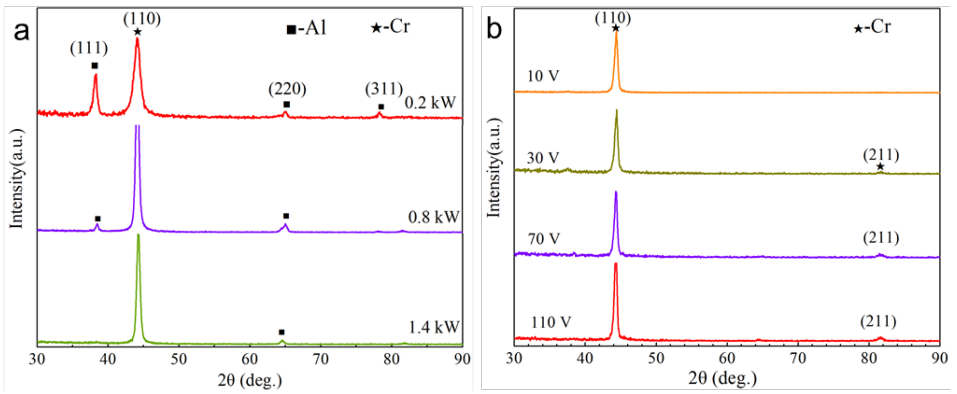
Figure 2.
Top surface images of Cr films deposited at different power on surface of 2024 Al alloy: (a,b) 0.2 kW, (c,d) 0.8 kW, (e,f) 1.4 kW (the left and right side are low and high magnifications, respectively).
Figure 2.
Top surface images of Cr films deposited at different power on surface of 2024 Al alloy: (a,b) 0.2 kW, (c,d) 0.8 kW, (e,f) 1.4 kW (the left and right side are low and high magnifications, respectively).

Figure 3.
Average column size of Cr films deposited with different power on surface of 2024 Al alloy.
Figure 3.
Average column size of Cr films deposited with different power on surface of 2024 Al alloy.

Figure 4.
Top surface images of Cr films deposited at different bias on surface of 2024 Al alloy: (a,b) 10 V, (c,d) 30 V, (e,f) 70 V, (g,h) 110 V (the left and right side are low and high magnifications, respectively).
Figure 4.
Top surface images of Cr films deposited at different bias on surface of 2024 Al alloy: (a,b) 10 V, (c,d) 30 V, (e,f) 70 V, (g,h) 110 V (the left and right side are low and high magnifications, respectively).

Figure 5.
Average column size of Cr films deposited with different bias on surface of 2024 Al alloy.
Figure 5.
Average column size of Cr films deposited with different bias on surface of 2024 Al alloy.
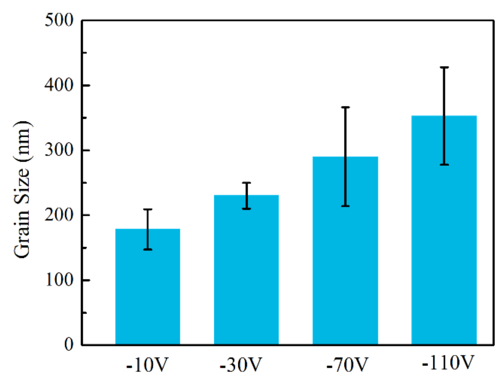
Figure 6.
Cross-section and fracture morphologies of Cr films deposited at different power on surface of 2024 Al alloy (a,b) 0.2 kW, (c,d) 0.8 kW, (e,f) 1.4 kW (the left is polished morphology and the right is fracture morphology).
Figure 6.
Cross-section and fracture morphologies of Cr films deposited at different power on surface of 2024 Al alloy (a,b) 0.2 kW, (c,d) 0.8 kW, (e,f) 1.4 kW (the left is polished morphology and the right is fracture morphology).
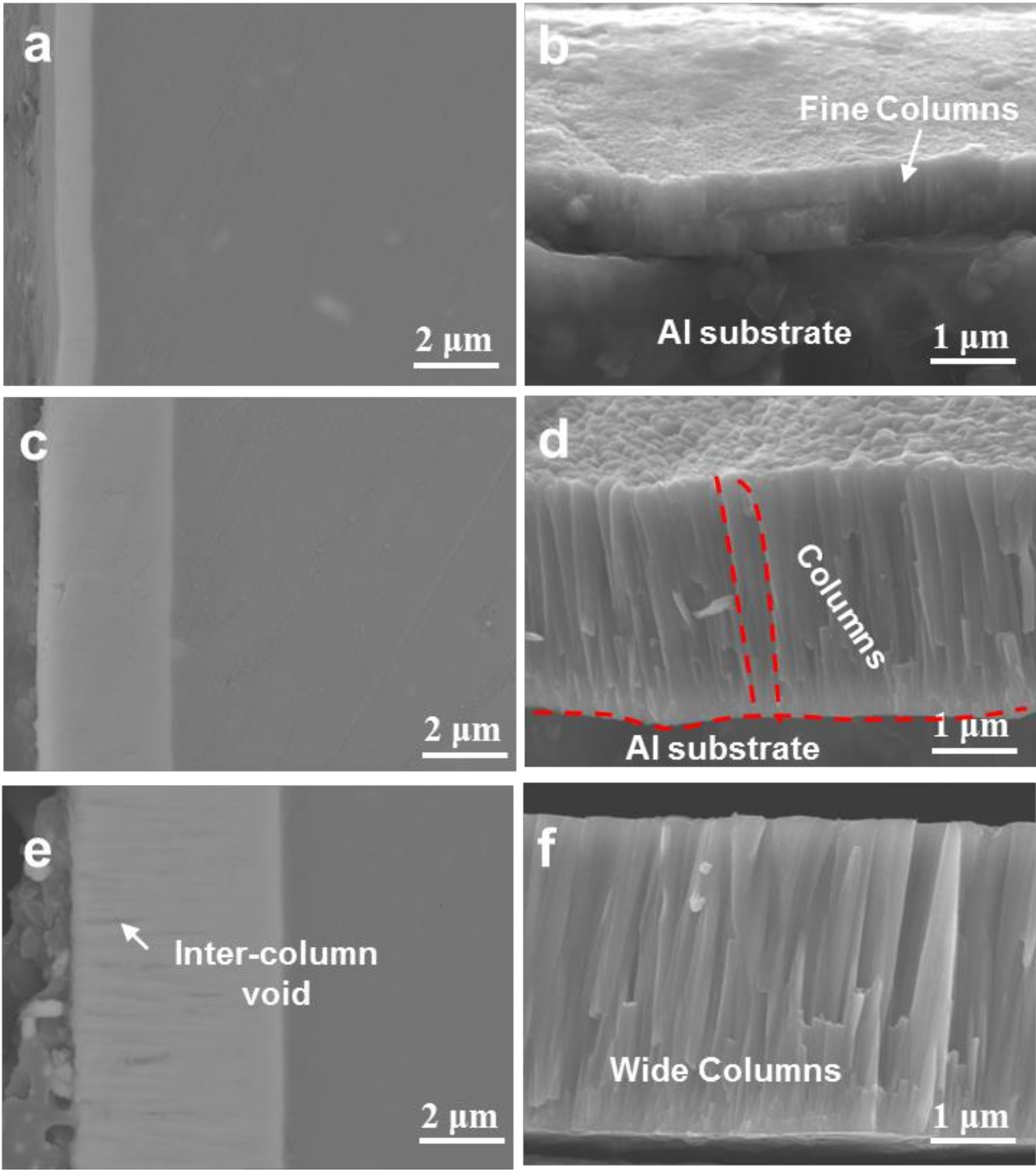
Figure 7.
Cross-section and fracture morphologies of Cr films deposited at different bias on surface of 2024 Al alloy: (a,b) 10 V, (c,d) 30 V, (e,f) 70 V, (g,h) 110 V (the left is polished morphology and the right is fracture morphology).
Figure 7.
Cross-section and fracture morphologies of Cr films deposited at different bias on surface of 2024 Al alloy: (a,b) 10 V, (c,d) 30 V, (e,f) 70 V, (g,h) 110 V (the left is polished morphology and the right is fracture morphology).
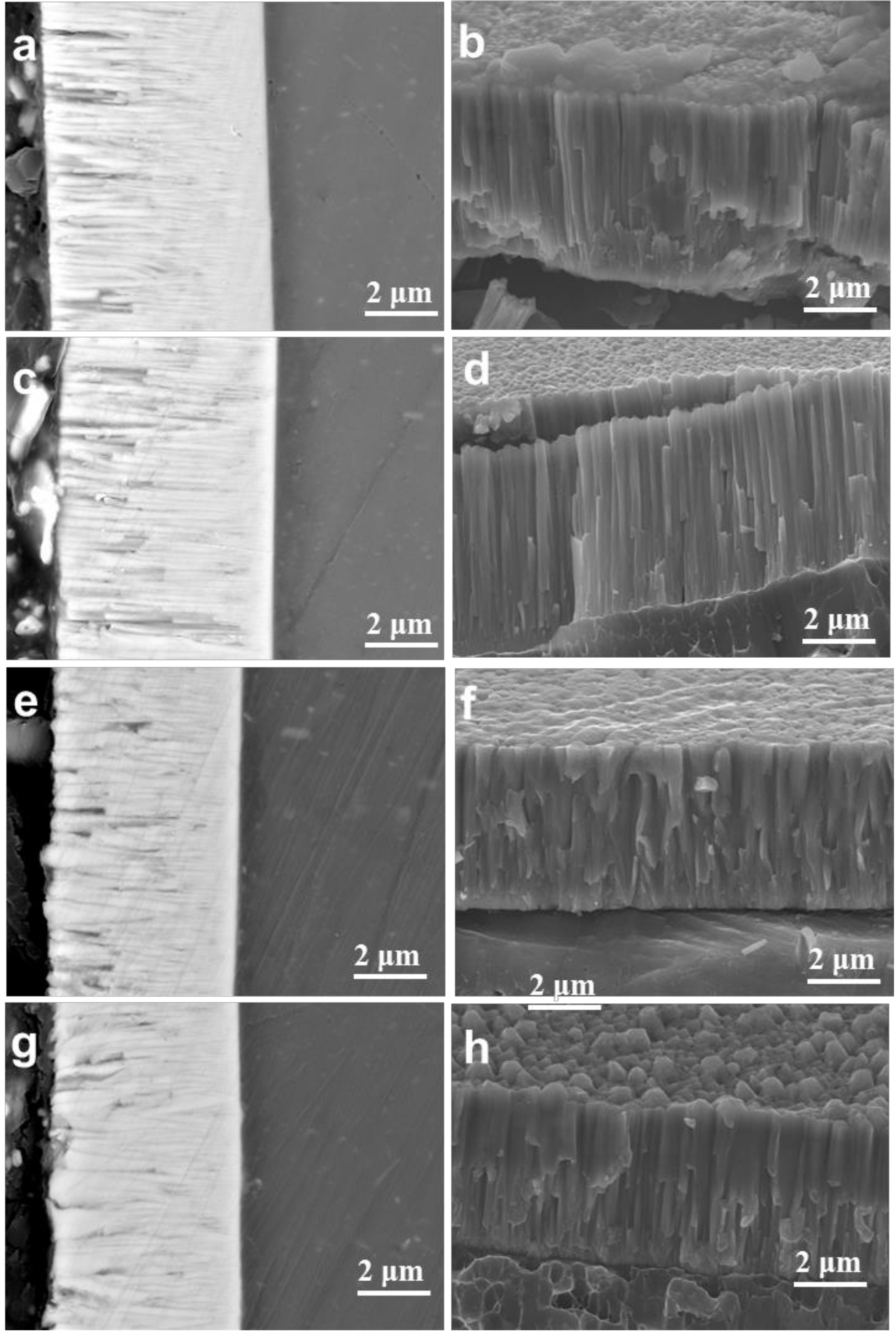
Figure 8.
Load-depth curves of Cr films under micro-indentation condition.

Figure 9.
Acoustic emission (AE) signal corresponding to applied load curves of Cr films deposited at (a) different powers and (b) different biases.
Figure 9.
Acoustic emission (AE) signal corresponding to applied load curves of Cr films deposited at (a) different powers and (b) different biases.
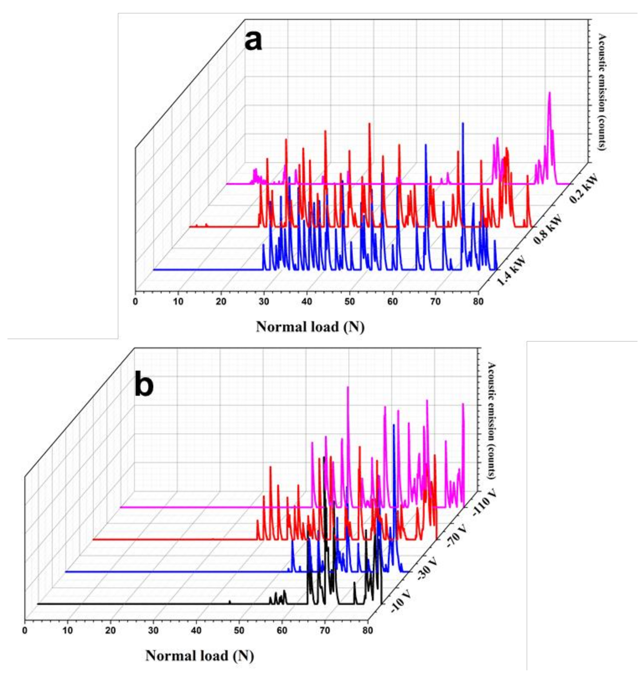
Figure 10.
Representative morphologies of scratch track of Cr films deposited at 2.0 kW/70 V: (a) whole track, (b,f) partial track of I, (c,g) partial track of II, (d,h) partial track of III, (e,i) partial track of IV.
Figure 10.
Representative morphologies of scratch track of Cr films deposited at 2.0 kW/70 V: (a) whole track, (b,f) partial track of I, (c,g) partial track of II, (d,h) partial track of III, (e,i) partial track of IV.
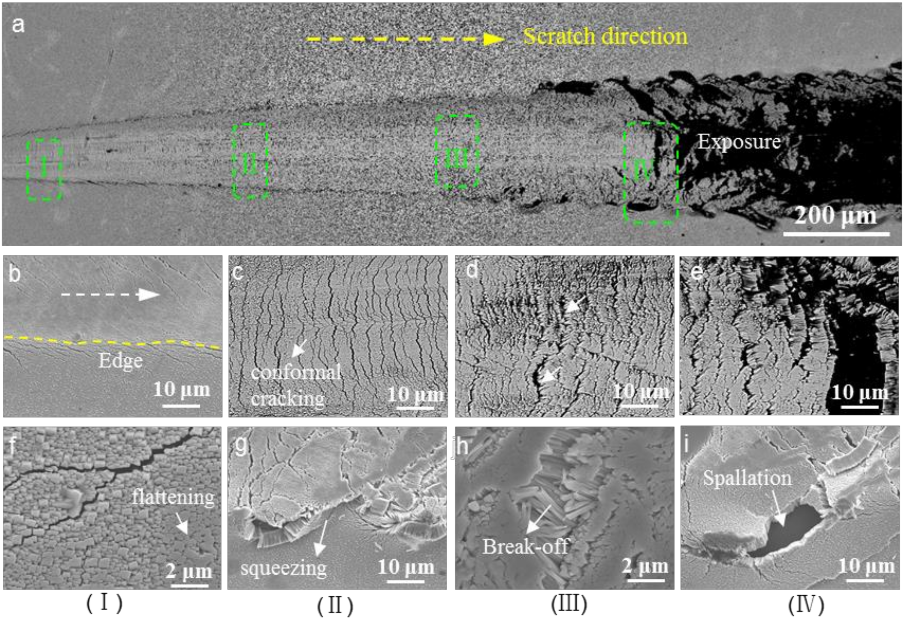
Figure 11.
Detailed SEM observations in the scratch track: (a) tensile cracking, (b) plastic deformation of Al substrate, (c) columns buckling, (d) pushing down columns.
Figure 11.
Detailed SEM observations in the scratch track: (a) tensile cracking, (b) plastic deformation of Al substrate, (c) columns buckling, (d) pushing down columns.
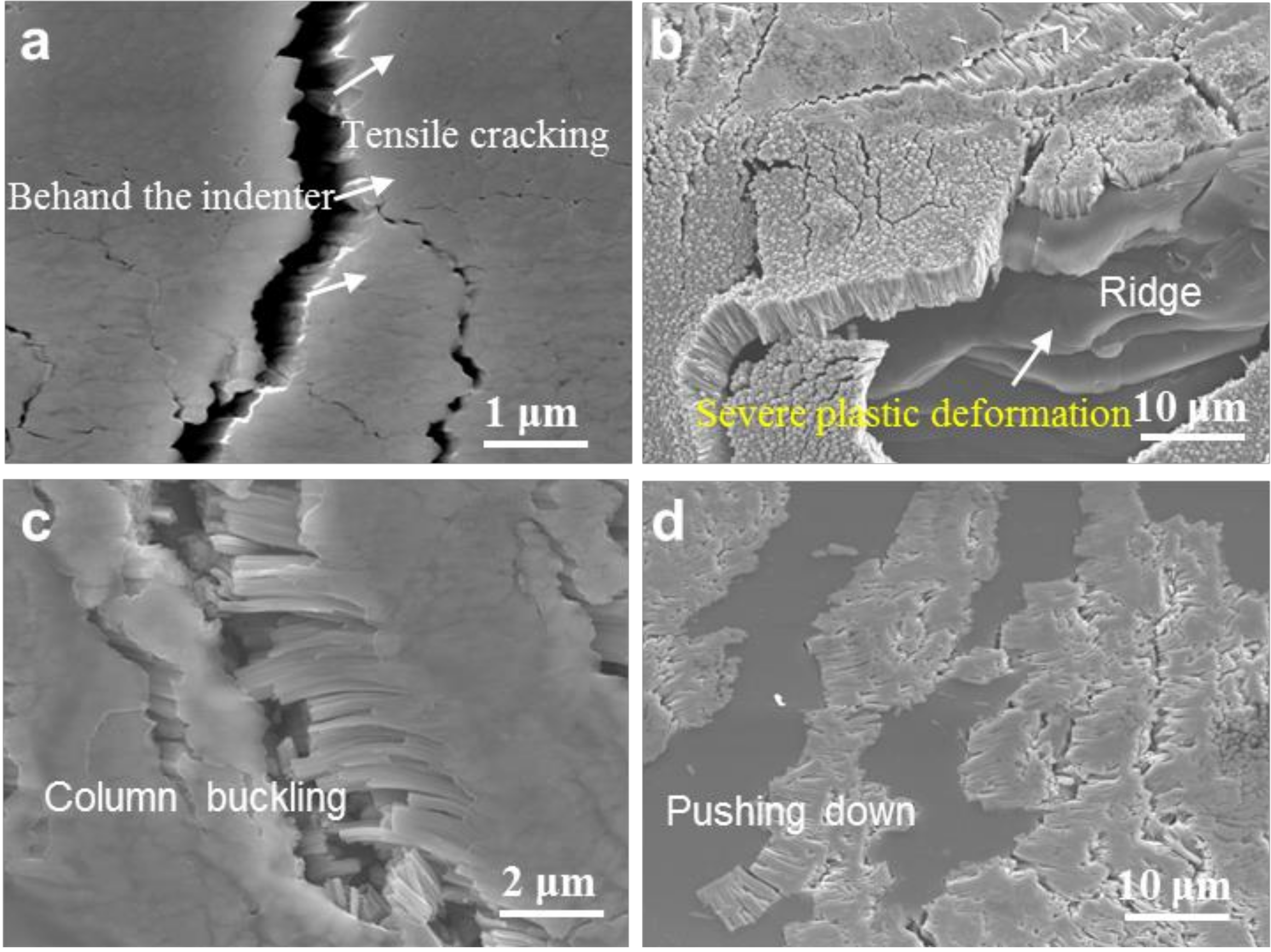
Figure 12.
Schematic failure mechanism of deposited Cr films under scratch testing.


Table 1.
Deposition parameters of Cr films by using magnetron sputtering.
| Sample | Cr Power (kW) | Bias (V) | Sputtering Time (h) | Sputtering Pressure (Pa) | Argon Flux (sccm) |
|---|---|---|---|---|---|
| DC1 | 2.0 | 10 | 2 | 0.2–0.3 | 16 |
| DC2 | 2.0 | 30 | 2 | 0.2–0.3 | 16 |
| DC3 | 2.0 | 70 | 2 | 0.2–0.3 | 16 |
| DC4 | 2.0 | 110 | 2 | 0.2–0.3 | 16 |
| DC5 | 0.2 | 70 | 2 | 0.2–0.3 | 16 |
| DC6 | 0.8 | 70 | 2 | 0.2–0.3 | 16 |
| DC7 | 1.4 | 70 | 2 | 0.2–0.3 | 16 |
Table 2.
Micro-indention results of 2024 Al alloy and Cr films.
| Sample | H (GPa) | E (GPa) | Wt (nJ) | Wp (nJ) | ηp | H/E | H3/E2 |
|---|---|---|---|---|---|---|---|
| 2024 Al | 1.44 | 90 | 0.682 | 0.643 | 0.94 | 0.016 | 0.0003 |
| DC1 | 3.81 | 130 | 0.371 | 0.322 | 0.86 | 0.0293 | 0.0032 |
| DC2 | 3.60 | 129 | 0.389 | 0.346 | 0.89 | 0.0279 | 0.0028 |
| DC3 | 4.56 | 167 | 0.314 | 0.247 | 0.78 | 0.0273 | 0.0034 |
| DC4 | 4.87 | 169 | 0.317 | 0.292 | 0.92 | 0.0288 | 0.0040 |
| DC5 | 3.31 | 81.5 | 0.518 | 0.431 | 0.83 | 0.0406 | 0.0054 |
| DC6 | 4.19 | 127 | 0.363 | 0.297 | 0.81 | 0.0328 | 0.0045 |
| DC7 | 4.33 | 164 | 0.347 | 0.286 | 0.82 | 0.0264 | 0.0030 |
© 2019 by the authors. Licensee MDPI, Basel, Switzerland. This article is an open access article distributed under the terms and conditions of the Creative Commons Attribution (CC BY) license (http://creativecommons.org/licenses/by/4.0/).
Share and Cite
MDPI and ACS Style
Ding, Y.; Zhang, F.; Yan, S.; Li, H.; He, J.; Yin, F. Microstructure, Micro-Indentation, and Scratch Behavior of Cr Films Prepared on Al alloys by Using Magnetron Sputtering. Metals 2019, 9, 1330. https://doi.org/10.3390/met9121330
AMA Style
Ding Y, Zhang F, Yan S, Li H, He J, Yin F. Microstructure, Micro-Indentation, and Scratch Behavior of Cr Films Prepared on Al alloys by Using Magnetron Sputtering. Metals. 2019; 9(12):1330. https://doi.org/10.3390/met9121330
Chicago/Turabian StyleDing, Yi, Fanyong Zhang, Shu Yan, Hongtao Li, Jining He, and Fuxing Yin. 2019. "Microstructure, Micro-Indentation, and Scratch Behavior of Cr Films Prepared on Al alloys by Using Magnetron Sputtering" Metals 9, no. 12: 1330. https://doi.org/10.3390/met9121330
Note that from the first issue of 2016, this journal uses article numbers instead of page numbers. See further details here.