Wettability and Infiltration of Liquid Silicon on Graphite Substrates


1
Solidification Processing and Engineering, IMDEA Materials Institute, Eric Kandel 2, Getafe, 28906 Madrid, Spain
2
Materials Science and Engineering Department, Universidad Carlos III de Madrid, 28911 Leganés, Spain
*
Author to whom correspondence should be addressed.
Metals 2019, 9(3), 300; https://doi.org/10.3390/met9030300
Submission received: 28 January 2019
/
Revised: 19 February 2019
/
Accepted: 21 February 2019
/
Published: 6 March 2019
Abstract
:The energy crisis has stimulated a rapid growth of developments in the photovoltaic industry in recent years. To reduce the high cost and the toxicity of classical metallurgical routes, new methods, such as vacuum refining of silicon, have been developed. Moreover, at the industry level, parameters such as the porosity in crucibles and dies are not controlled, so wettability, infiltration, and reaction between silicon and graphite are the key factors in the purification process. In this work, the behavior of several refractory substrates against melted silicon was studied by the classic sessile drop method. The most important phenomena, i.e., wettability and infiltration, were compared with the properties of the substrates. According to the results, for the carbonaceous materials, the reaction of triple line silicon-graphite manages these phenomena, whereas for alumina, a passive layer is formed due to the presence of oxygen, which is subsequently eliminated by the chemical reactions, delaying the process. Regarding the contact angle and infiltration behavior, alumina showed the best results, but due to its reactivity, it contaminates Si, so that this material is not recommended for solar silicon application. However, composite 2 is compatible with the application, as it shows good results in comparison with the other materials.
1. Introduction
In recent years, there has been a rapid growth in the development of the photovoltaic industry (PV). Photovoltaic energy is considered as a main renewable electric source, and silicon is considered as the dominant material for the fabrication of solar cells, so that solar-grade silicon (SGS) feedstock is more and more needed [1,2].
The photovoltaic properties of silicon depend on the concentration of individual impurities, so the acceptable levels are defined by the conversion efficiency of solar cells. Depending on the degree of purity, silicon is classified into three main groups: electronic grade silicon (EGS) (10−4–10−5 ppm impurities), solar grade silicon (SGS) (10−1–10−2 ppm impurities), and metallurgical grade silicon (MGS) (~103 ppm impurities) [3].
Traditionally, recycled EGS has been used by the photovoltaic (PV) industry. Currently, as its demand is ever increasing, metallurgical grade silicon is purified with this aim. The main routes to obtain SGS from MGS are chemical and metallurgical processes. Chemical processes are modifications of the Siemens process, whose major drawbacks are high cost and toxicity [1,3]. On the other hand, the metallurgical route combines different metallurgical methods to obtain the required purity grade [3]. For example, vacuum refining of molten silicon is used to eliminate volatile elements from liquid silicon, such as P, Al, Ca, and Mn [4], while boron and other metallic impurities are removed by directional solidification and plasma treatment [5].
Besides the elimination of the impurities from metallurgical silicon, it is also important to avoid the contamination of silicon with elements from the furnace during the purification. Graphite is often used for crucibles, substrates, and dyes in several stages of processing of SGS by metallurgical routes [6]. It has advantages such as high-temperature stability and good machinability. In addition, the electrical effects of dissolved carbon in the PV cells are negligible. However, the reactivity between Si and graphite can be a determining factor of the lifetime of graphite crucibles. Moreover, the open porosity increases this disadvantage [7].
In order to avoid the impurities, inert materials not-wetted by silicon are required. Nevertheless, such materials have not been found yet because molten silicon is very reactive. Hence, wetting and infiltration of molten silicon into the refractories should be minimized [7]. In addition to silicon purification, knowledge about wetting and infiltration of silicon in graphite is relevant for techniques such as reaction bonding of silicon carbide (RBSC) and liquid silicon infiltration (LSI) [8].
For porous graphite substrates, wettability and infiltration are managed by the reactions along the triple line (vapor, liquid, and solid) [9]. It is known that the reaction between silicon and graphite allows the phenomena of wetting and infiltration. Wettability depends on the roughness [10], temperature [11], atmosphere [12], open porosity, and type of substrate [7]. Since the exact influence of each factor is still not known, there is a large scatter of results [6,7,8,9,10,11]. Molten silicon initially does not wet carbonaceous materials. However, owing to the reactivity between Si and C, a SiC layer is formed that strongly enhances the wettability [7]. Perfect wettability (angle contact equals zero) is found in substrates with both a high surface roughness and a large average pore size [7]. Nevertheless, there is no accurate knowledge about the key factors governing infiltration kinetics [13]. It is known that infiltration does not vary according to Washburn’s equation because it is controlled by the formation of a SiC layer at the triple line of the infiltration front and not by viscous resistance. However, there is no theoretical model that describes this process, despite the existence of several studies [6,7,8,9].
The purpose of this paper is to investigate and understand the interaction processes between molten silicon and different substrates through the analysis of wetting and infiltration processes.
2. Materials and Methods
The behavior of several substrates against molten silicon was studied. The most important phenomena studied were wettability, infiltration, and reactivity. The studied substrate materials were graphite, carbon composite (tagged as 1), carbon composite (tagged as 2), and high purity alumina. The graphite and composites 1 and 2 were provided by Ferrosolar, and the high purity alumina was provided by Magnesita (Hindel, Germany).
First, the density of the substrates was measured by Archimedes method in order to determine the percentage of open porosity. Then, the substrates were analyzed by tomography in an X-ray computer-assisted 3D nanotomography scanner (Nanotom, Phoenix, AZ, USA) to analyze the size and distribution of the pores. Finally, a Raman micro-spectroscopy system (Renishaw PLC, Wotton-under-Edge, Gloucestershire, United Kingdom) was used in order to study their crystallinity.
Wettability and infiltration were measured using the sessile drop method, which consists of melting a silicon drop (about 50 mg mass) directly on a substrate while it is recorded by a high speed video camera (Drop Shape Analysis for High Temperatures, Krüss GmbH, Hamburg, Germany). Then, the main parameters, such as contact angle and height and width of the drop, were measured by using specific software. The equipment used was a Krüss DSAHT (Drop Shape Analysis for High Temperatures, Krüss GmbH, Hamburg, Germany) as schematically shown in Figure 1. The substrates were slices with dimensions of 15 × 15 × 5 mm3.
After that, the formed phases were examined by a Philips X’Pert X-ray diffractometer (Malvern panalitycal, Grovewood Road, Malvern, United Kingdom) with copper anode. The working conditions were 40 kV/40 mA. Finally, the samples were prepared for metallographic and chemical analysis, by using light optical microscopy (LOM) and scanning electron microscopy (SEM, EVO MA15, Zeiss, Birkerød, Denmark) with chemical microanalysis (EDS, Oxford INCA 350, Oxford Instruments plc, UK, Magnetic Resonance, NanoScience, Abingdon, UK).
To analyze the kinetics of the process, the infiltration rate Uinf (Uinf = −dh/dt) and spreading rate Uspr (Uspr = dR/dt) were calculated, where h and r are the height and half of the width of the drop, respectively. They were obtained by in situ analysis of the sessile drop. The decrease in height is due to the infiltration and spreading, but it was supposed that it is only due to infiltration for these calculations.
3. Results
This section may be divided by subheadings. It should provide a concise and precise description of the experimental results, their interpretation, as well as the experimental conclusions that can be drawn.
3.1. Porosity Analysis
The open porosity and total density were measured by Archimedes method, and the results are shown in Table 1. Every material has an open porosity, and the maximum is in composite 1 and the minimum in graphite.
The porosity has also been measured by image analysis obtained by tomography, and the results are rather similar to the results of the Archimedes method. The differences are due to the error of each method.
In addition, the porosity was determined by tomography. The distribution of pores is shown in Figure 2.
The porosity in the graphite is homogeneously distributed throughout the material. However, the alumina has porosity mostly at the grain boundaries. On the other hand, the porosity of composite materials depends on the packing direction of the fibers.
3.2. Crystallinity Analysis
According to Beyssac et al. [15], the crystallinity of carbonaceous materials can be analyzed and even quantified by Raman microspectroscopy. Figure 3 shows the typical Raman spectrum of a carbonaceous material [15].
The G band indicates the vibrational mode E2g. A narrow and high intensity G peak is characteristic for a material with a high degree of crystallinity, while a wide and low intensity G peak indicates amorphous materials. The D band indicates structural disorder. The D1 band has a high intensity and width in disordered materials; D2 in amorphous materials is not distinguishable from the G band, and D3 is present in amorphous material as a wide band.
To quantify the grade of crystallinity, Beyssac et al. [15] proposed the ratio D1/(D1 + D2 + G), where the parameters represent the area of the bands. The lower the value of this ratio, the higher is the grade of crystallinity.
Table 2 shows the results of the ratio D1/(D1 + D2 + G) for the substrates, where the values were calculated by the average of different points.
Regarding the results in Figure 4, we can observe that graphite and composite 2 have a higher grade of crystallinity as the G band has a high intensity and is narrow. Also, the ratio is lower than 0.5; thus, they can be considered crystalline materials, although the D1 band indicates that both materials have several defects. On the other hand, composite 1 is an amorphous material due to having a ratio higher than 0.5, a higher and wider D band, and because the D2 band is difficult to distinguish from the G band.
According to Eustathopoulos et al. [16], the wettability on carbonaceous materials depends on the grade of crystallinity. Amorphous materials lead to difficulty of the reaction between silicon and graphite due to the interruption by impurities; thus, the wettability becomes worse. Because of this interruption of the reaction in the triple line, Caccia et al. suggested that the crystallinity can also have an effect on the infiltration [13].
3.3. Sessile Drop Tests
Figure 5 shows images captured during the sessile drop tests. The images of the most important moments were isolated from the video sequence recorded.
Silicon starts to melt at the bottom of the sample, which is the area in contact with the substrates. When the silicon is totally molten, the drop is formed. Then, the contact angle decreases due to the spreading and the infiltration until silicon is completely infiltrated in the substrate (Figure 5). For graphite, composite 1, and composite 2, the silicon drop infiltrates the substrate completely in less than 3 min. However, in the case of alumina, it can be seen that unlike the other materials, the spreading is only slight and the infiltration is completed after 28 min.
In Figure 6, the variation of the contact angle and silicon drop height and width with time is shown for all materials. The time origin always corresponds to the moment when the drop is completely formed. Figure 6a shows the case for the graphite substrate. The decrease in the contact angle and height and the increase in the width with time are totally linear. In addition, the process can be divided into two stages: the first one is when the silicon sample starts to melt until the drop is formed, and the second one is from the time when the drop is formed until the silicon is totally infiltrated. In both stages, infiltration and spreading happened. The spreading was managed by the reaction between silicon and graphite.
Si + C = SiC,
This is in agreement with many authors, for example, Israel [17]. However, this same study asserts that the infiltration finishes when the pores of the substrate are closed, but in our case, the silicon infiltrates totally and then closure of the pores happens by the formation of silicon carbide due to the large size of the pores.
Silicon was melted on graphite under argon atmosphere using the sessile drop test. The roughness of graphite was 4.83 µm, and the initial contact angle obtained was 23.6° at 1424 °C. According to the references (Table 3), the results are quite different. The variation in the contact angle values can be because the test conditions are not similar (roughness, temperature, and atmosphere), and the roughness and pore size show the most remarkable differences.
The behavior of the molten silicon on alumina is highly dependent on the possible formation of a passive layer of SiO2 on the substrate. The spreading and infiltration on alumina can be divided into three stages (Figure 6b). First, the contact angle decreases, the width increases, and the height remains almost constant (stage I). This behavior can be related to the formation of the passive layer. Then, the contact angle and the height almost linearly decrease while the width increases until a maximum (stage II). In this stage, the passive layer starts to break until it has been totally removed, and the contact angle and drop width and height dramatically decrease until the drop disappears through infiltration. Silicon was melted on alumina under argon atmosphere using the sessile drop test. The initial contact angle obtained was 86.2° at 1424 °C. According to the Yuan et al. [18], this result is in agreement (86° at 1422 °C under argon atmosphere). Moreover, the spreading was minimum and infiltration was slower than on the other substrates, but the silicon infiltrated completely due to the high porosity of alumina. This good behavior against molten silicon can be due to the possible formation of the above-mentioned passive layer of SiO2. The problem happened when the layer was broken and the infiltration was dramatically fast.
The variation in the contact angle and the parameters of the drop (height and width) with time for the silicon drop on composite 1 is shown in Figure 6c. Because of the high variation in the data of the contact angle and width, a moving average filter was applied. The width remains almost constant, possibly due to the high roughness. However, two stages are shown with regard to the contact angle and height. Both magnitudes decreased much faster in the second stage than in the first one. The change in slope is remarkable. Silicon was melted on composite 1 under argon atmosphere using the sessile drop test. The initial contact angle obtained was 27.9° at 1425 °C.
On the other hand, Figure 6d shows the variation in the contact angle of composite 2. The height and width of the drop were measured with respect to time. Similar to graphite, once the drop is formed, the width linearly increases while the height and contact angle linearly decrease. The spreading is driven by the chemical reaction between Si and C, as described by Equation (1). Silicon was melted on composite 2 under argon atmosphere using the sessile drop test. The initial contact angle obtained was 43.8° at 1422 °C. Similar to the other carbon materials, two parts are distinguished: the first one is governed mainly by infiltration and the second by spreading.
3.4. Wettability, Infiltration and Reactivity
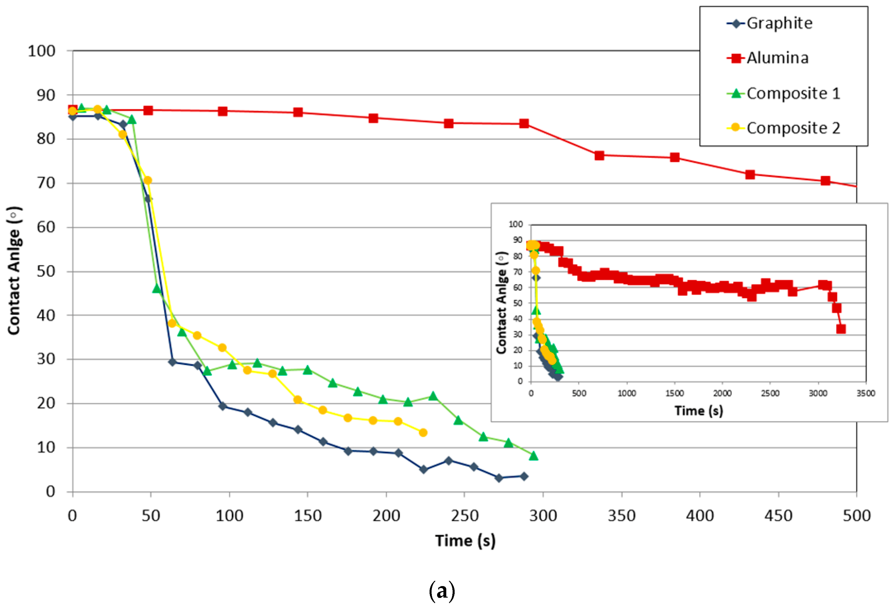
The variation of the contact angle and relative height (mm/mm) of the drop on different substrates (graphite, alumina, and composites) with time is compared in Figure 7.
Figure 7a compares the variation of the contact angle of all studied materials with time, once the drop was formed. First, the wettability of silicon on alumina is much lower than on the other materials. Alumina shows the highest contact angle in comparison to the other substrates. Additionally, the contact angle decreased much slower than on the other materials with time and temperature.
On the other hand, the contact angle of graphite linearly decreased in contrast to the composites where there was a change in slope. The slopes of the curves indicate that the contact angle of composite 2 decreases faster than that of the graphite and composite 1, whose slopes are very similar. This can indicate that the silicon–carbon reaction controls the triple line, and in the case of composite 2, it is possible that some scratches or irregularities of the surface improved the spreading, due to the fact the liquid move easily in the direction of the cracks.
Figure 7b shows the variation of the relative height (mm/mm) of different materials with the time. The data were collected when the silicon started to melt. The height was divided by the initial height in order to compare the values.
Since the melting starts at the bottom of the sample, infiltration and spreading are key factors in this stage, and the materials with relevant porosity will be infiltrated deeper than those whose surfaces boost the spreading.
As in the case of wettability, the infiltration in alumina was much slower than in the other materials. However, silicon infiltrated entirely in alumina, and in addition, the infiltration was faster with the increment of time.
For the carbonaceous materials, graphite and the composites show a remarkable change of slope. Before the drop, the reduction of height for composite 2 is slower than that for graphite and composite 1. However, after the drop, composite 2 and graphite are faster than composite 1. Observing the behavior of the composites, as in the case of graphite, the carbon-silicon reaction manages the reaction despite the change in the direction of the fibers that produce some modifications.
The infiltration rate Uinf and spreading rate Uspr were calculated for different substrates in each stage of the process (Table 4). For graphite, they were calculated before and after the drop formation. The spreading was faster than the infiltration both before and after the formation of the drop. The kinetics rate agrees that the process is governed by chemical reaction at the triple line [19].
In the case of alumina, spreading was faster than infiltration in the first stage, with both values being low. Then, in the second stage, the infiltration increased sharply while the spreading decreased slightly. These results support the formation and subsequent breakage of a passive layer of SiO2.
For composite 1, while the drop was forming, the spreading was slower than the infiltration. Then, both rates decreased; in particular, the spreading rate remained almost constant. In the second stage, the rates had the same order of magnitude, but the spreading is a bit faster than infiltration. In comparison with the behavior of graphite, some similarities were found. This indicates that spreading and infiltration is managed by the reaction at the triple line, but the roughness affected these phenomena.
For composite 2, in the first stage, spreading was faster than infiltration. Then, the spreading decreased and infiltration increased. As in the case of graphite, the results agree with the fact that the reaction (Equation (1)) manages the spreading and the infiltration of silicon on the substrate.
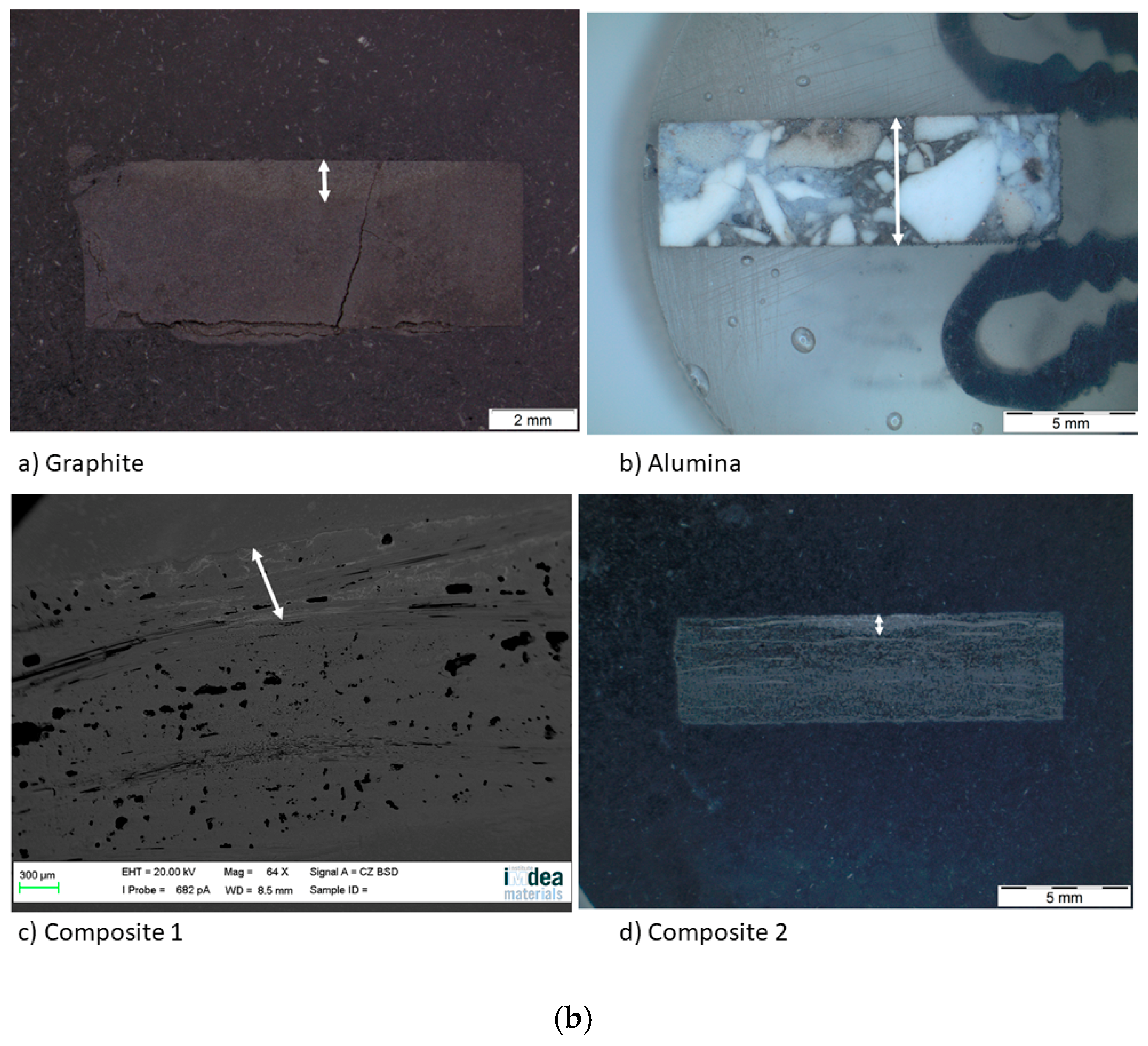
After the sessile drop test, the top view images were taken by an optical microscope (Figure 8a). Then, the substrates were cut and the side view images were also taken (Figure 8b), except for composite 1, because a high resolution was needed. For this purpose, a scanning electron microscope was used. Regarding the spreading, the effective radius R was calculated from the wetted area A (A = πR2), which was measured by image processing for each material. This technique was also used to measure the infiltration distance (Table 5).
The wetted area can be divided into two concentric circles on the graphite and the composite materials. The smallest one matches with the area of the maximum infiltration distance and the biggest one with the maximum spreading area. On the other hand, on the alumina material, there is a single circle and the silicon has infiltrated the whole substrate.
In addition, the maximum radius was measured in situ by the sessile drop method and is included in Table 5.
The fact that the circles are not symmetric indicates that any defect pinned the drop, decreasing the formation of the SiC layer but increasing the diffusivity of silicon in certain directions. According to Table 5, the values of the maximum radius and the external radius are different. This fact is probably because the drop is not symmetric; thus, the size of the radius depends on the direction where it was recorded. On the other hand, another cause could be secondary wetting [9], i.e., a parallel infiltration that takes place after the spreading time.
Regarding the infiltration, it is pointed out that the infiltration distance of composite 1 is the minimum in spite of its high grade of porosity. This fact agrees with the high rugosity and low grade of crystallinity. Both features make the infiltration very difficult. However, the infiltration distance in the alumina is the maximum because of the high grade of porosity.
On the other hand, a thin silicon carbide layer is produced on the surface (Figure 9a). In Figure 9b, we can see the micrographs of alumina after the sessile drop test where silicon has infiltrated inside the cracks of alumina, so that oxygen has been able to pollute the silicon, despite the X-ray results shown in Figure 10 not revealing the formation of silicon oxide (Figure 11). In Figure 9c, the micrographs of composite 1 after the sessile drop test are shown where silicon has infiltrated between and has reacted with the carbon fibers. According to Figure 6 and Figure 12, there is no unreacted silicon. This means that the reaction in the triple line is a key factor in spite of the roughness. Figure 9d shows the micrographs of composite 2. Silicon has infiltrated through the cracks of composite 2 and reacted with carbide, but unreacted silicon has been found (Figure 13). In accordance with Novakovic et al. [20], 10% of silicon remains unreacted when Si/C composites are obtained by the infiltration method. Regarding the reactivity of graphite, it can be highlighted that the graphite shows pores that are almost closed, and there is no unreacted silicon, as confirmed by the X-ray results (Figure 10).
4. Discussion
In Table 6, it can be observed for the case of graphite that the phenomena of infiltration and spreading are managed by the reaction between silicon and carbon at the triple line. However, in the cases of the composites, it is more complicated to obtain this conclusion.
First, graphite and composite 2 show a linear relation of the contact angle and the parameter of the silicon drop with time. In contrast, composite 1 shows a remarkable change in the slope. According to Drevet et al. [21], the initial contact angle of silicon on graphite is around 90°, which corresponds to Si-C wetting, and the contact angles obtained around 20°–40° correspond to Si-SiC layer wetting. Before melting, silicon evaporates and forms a silicon carbide layer, which dramatically decreases the contact angle. The initial contact angles observed for graphite substrate (23.6°), composite 1 (27.69°), and composite 2 (43.8°) indicate Si-SiC wetting. This seems to be in disagreement with Li and Hausner [10], whose results showed that the contact angle was smaller due to the high roughness. However, in spite of the calculated Ra, composite 2 was less rough than the graphite substrate, but it had large holes that affected the average result.
In addition, Caccia et al. [13] proposed values of the spreading rate Uspr (dR/dt) at around 10 μm/s in a system managed by reaction at the triple line. Additionally, they concluded that the value of rate infiltration and the rate of spreading have to be similar, so that Uinf/Uspr = (0.65–0.95). The graphite and composite 2 results agree with the values proposed by Caccia et al. [13] for systems managed by reaction in the triple line. However, the values of composite 1 are out of this range. The reaction in the triple line can be hindered by pollution or roughness of the substrate.
Regarding the top and side views of the carbonaceous substrates, the results suggest that the more the silicon spreads, the less the substrates will be infiltrated, independent of the roughness, porosity, or average pore diameter. Israel et al. [6] affirmed that the infiltration ends when the pores are closed. In our case, the pores are big so that silicon infiltrated thoroughly, and then the pores were closed only after infiltration. Thanks to that, silicon reacted totally. These results are remarkable because the main disadvantage of reaction bonded silicon carbide (RBSC) is that the final material contains unreacted silicon [13].
On the other hand, SEM and X-ray analyses reveal a silicon carbide layer on the surface of the graphite and closed pores for the graphite substrate and composite 1. In addition, there are no significant impurities in the composites. However, the X-ray results show unreacted silicon on the surface of composite 2, and according to Novakovic et al. [20], 10% of silicon does not react when Si/C composites are obtained by the infiltration method.
In spite of the differences with the graphite substrate, composite 1 and composite 2 are managed by the reaction in the triple line. In the case of composite 1, the different directions of the fibers boosted the spreading and hindered the infiltration and the reaction in the triple line. On the other hand, according to Eustathopoulos et al. [9], the infiltration rate is equal to infiltration spreading divided by the tortuosity factor, ξ.
dh/dt = (dR⁄dt)/ξ,
The tortuosity is defined as the ratio between the way chosen by a fluid lying inside a porous body and the geometrical distance between two points. Besides, they related the tortuosity factor to the inverse of the porosity of the substrate. However, we did not find any relation between the porosity or average pore size with the infiltration rate or maximum distance infiltrated.
The behavior of silicon on the alumina substrate was completely different. This system is likely governed by the formation and the breakage of a passive layer of SiO2. According to Drevet et al. [21], molten silicon can dissolve the oxygen of alumina and after saturation, precipitate as SiO2. The SiO2 forms a passive layer that avoids the infiltration.
Si (S or L) + O2 (G) ↔ SiO2 (S),
However, the breakage of the passive layer is possible because molten silicon can dissolve the oxides following Equation (4):
Thanks to argon flow, the oxides can be evacuated. At the same time, the same process happens on the wall of the pores of alumina. First, a passive layer is formed on the wall of the pores and the infiltration is hindered, but when the passive layer is eliminated, the infiltration started. The infiltration depends on the evacuation of the oxides. This process is slow, although at the beginning, it is lower than at the end because of the quantity of molten silicon. The initial contact angle calculated in this study agrees with the literature [21]. This material is not used in the solar silicon industry due to the pollution of silicon.
5. Conclusion
The behavior of several substrates (graphite, carbon composites, and high purity alumina) against melted silicon was studied by classic Sessile drop method [6]. The most important phenomena, wettability and infiltration, were analyzed and compared with the properties of the substrates (porosity, roughness, crystallinity). From the obtained results the following conclusions may be drawn:
- The reaction of triple line silicon-graphite manages the phenomena of infiltration and wettability. This is showed by the linear variation of contact angle and parameters of silicon drop with the time in the substrates: Graphite, composite 1, and composite 2. However, the graphics of composite 1 indicated that the reaction has been hindered by the roughness. In the case of Alumina, due to the presence of oxygen, a passive layer is likely formed and subsequently eliminated by chemical reactions of silicon-oxygen [6,19], delaying the processes.
- Regarding contact angle and infiltration behavior, Alumina is the best material studied in this paper against molten silicon. However, regarding the reactivity, silicon was contaminated so that this material is not recommended for solar silicon application.
- Composite 2 is compatible with the application, as it shows a high initial contact angle, good behavior in spreading and infiltration in comparison with the other materials, and also contains unreacted silicon at the surface.
Author Contributions
Conceptualization, Srdjan Milenkovic and Jose Manuel Torralba; writing—original draft preparation, Almudena Casado; writing—review and editing, Srdjan Milenkovic and Jose Manuel Torralba.
Funding
This research was funded by Ferrosolar, grant number (RT_2016_SICASOL_04_02).
Acknowledgments
The authors wish to thank Ferroatlantica for financial support of the project and Magnesita for the materials. Also, Almudena Casado acknowledges the following people from Carlos III University of Madrid for the personal help and technical equipment: Elena Gordo, Paula Alvaredo, Monica Campos, Cristina Moral, Miguel Angel Marinez, Eric Macia, Andrea Galan, Alicia Paéz, and Amaya García.
Conflicts of Interest
The authors declare no conflict of interest.
References
- Lynch, D. Winning the global race for solar silicon. JOM 2009, 61, 41–48. [Google Scholar] [CrossRef]
- Binetti, S.; Libal, J.; Acciarri, M.; Di Sabatino, M.; Nordmark, H.; Øvrelid, E.J.; Walmsley, J.C.; Holmestad, R. Study of defects and impurities in multicrystalline silicon grown from metallurgical silicon feedstock. Mater. Sci. Eng. B 2009, 159–160, 274–277. [Google Scholar] [CrossRef]
- Safarian, J.; Tranell, G.; Tangstad, M. Processes for upgrading metallurgical grade silicon to solar grade silicon. Energy Procedia 2012, 20, 88–97. [Google Scholar] [CrossRef]
- Safarian, J.; Xakalashe, B.; Tangstad, M. Vacuum Removal of the Impurities from Different Silicon Melts. In Proceedings of the 26th European Photovoltaic Solar energy conference and exhibition, Hamburg, Germany, 5 September 2011; pp. 1810–1813. [Google Scholar]
- Flamant, G.; Kurtcuoglu, V.; Murray, J.; Steinfeld, A. Purification of metallurgical grade silicon by a solar process. Sol. Energy Mater. Sol. Cells 2006, 90, 2099–2106. [Google Scholar] [CrossRef]
- Israel, R.; Voytovych, R.; Protsenko, P.; Drevet, B.; Camel, D.; Eustathopoulos, N. Capillary interactions between molten silicon and porous graphite. J. Mater. Sci. 2010, 45, 2210–2217. [Google Scholar] [CrossRef]
- Ciftja, A.; Engh, T.A.; Tangstad, M. Wetting properties of molten silicon with graphite materials. Metall. Mater. Trans. A 2010, 41, 3183–3195. [Google Scholar] [CrossRef]
- Dezellus, O.; Jacques, S.; Hodaj, F.; Eustathopoulos, N. Wetting and infiltration of carbon by liquid silicon. J. Mater. Sci. 2005, 40, 2307–2311. [Google Scholar] [CrossRef]
- Eustathopoulos, N.; Israel, R.; Drevet, B.; Camel, D. Reactive infiltration by Si: Infiltration versus wetting. Scr. Mater. 2010, 62, 966–971. [Google Scholar] [CrossRef]
- Li, J.G.; Hausner, H. Wetting and infiltration of graphite materials by molten silicon. Scr. Metall. Mater. 1995, 32, 377–382. [Google Scholar] [CrossRef]
- Whalen, T.J.; Anderson, A.T. Wetting of SiC, Si3N4 and Carbon by Si and Binary Si Alloys. J. Am. Ceram. Soc. 1975, 396–399. [Google Scholar] [CrossRef]
- Rubio, P.J.Y.; Hong, L.; Saha-Chaudhury, N.; Bush, R.; Sahajwalla, V. Dynamic wetting of graphite and SiC by ferrosilicon alloys and silicon at 1550 °C. ISIJ Int. 2006, 46, 1570–1576. [Google Scholar] [CrossRef]
- Caccia, M.; Amore, S.; Giuranno, D.; Novakovic, R.; Ricci, E.; Narciso, J. Towards optimization of SiC/CoSi2 composite material manufacture via reactive infiltration: Wetting study of Si-Co alloys on carbon materials. J. Eur. Ceram. Soc. 2015, 35, 4099–4106. [Google Scholar] [CrossRef]
- Oro, R.; Campos, M.; Torralba, J.M. Study of high temperature wetting and infiltration for optimizing liquid phase sintering in low alloy steels. Powder Metall. 2012, 55, 180–190. [Google Scholar] [CrossRef]
- Beyssac, O.; Rouzaud, J.-N.; Goffé, B.; Brunet, F.; Chopin, C. Graphitization in a high-pressure, low-temperature metamorphic gradient: A Raman microspectroscopy and HRTEM study. Contrib. Mineral. Petrol. 2002, 143, 19–31. [Google Scholar] [CrossRef]
- Eustathopoulos, N.; Nicholas, M.G.; Drevet, B. Wettability at High Temperatures; Elsevier: Oxford, UK, 1999. [Google Scholar]
- Israel, R. Etude des interactions entre silicium liquid et graphite pour application à l’élaboration du silicium photovoltaïque. Available online: http://tel.archives-ouvertes.fr/tel-00434104/ (accessed on 22 February 2019).
- Yuan, Z.; Huang, W.L.; Mukai, K. Wettability and reactivity of molten silicon with various substrates. Appl. Phys. A 2004, 78, 617–622. [Google Scholar] [CrossRef]
- Camel, D.; Drevet, B.; Eustathopoulos, N. Capillarity in the processing of photovoltaic silicon. J. Mater. Sci. 2016, 51, 1722–1737. [Google Scholar] [CrossRef]
- Novakovic, R.; Giuranno, D.; Caccia, M.; Amore, S.; Nowak, R.; Sobczak, N.; Narciso, J.; Ricci, E. Thermodynamic, surface and structural properties of liquid Co-Si alloys. J. Mol. Liq. 2016, 221, 346–353. [Google Scholar] [CrossRef] [Green Version]
- Drevet, B.; Eustathopoulos, N. Wetting of ceramics by molten silicon and silicon alloys: A review. J. Mater. Sci. 2012, 47, 8247–8260. [Google Scholar] [CrossRef]
Figure 1.
Scheme of the equipment used for the wetting and infiltration experiments. The detail of the drop-substrate disposition is adapted from [14], with permission from Taylor & Francis, 2012.
Figure 1.
Scheme of the equipment used for the wetting and infiltration experiments. The detail of the drop-substrate disposition is adapted from [14], with permission from Taylor & Francis, 2012.

Figure 2.
Image of the distribution of pores in different materials, where (a), (b), (c), and (d) are graphite, alumina, composite 1, and composite 2, respectively.
Figure 2.
Image of the distribution of pores in different materials, where (a), (b), (c), and (d) are graphite, alumina, composite 1, and composite 2, respectively.

Figure 3.
Curve fitting of the first-order region of the Raman spectrum.

Figure 4.
Raman spectra of the first regions of the substrates: graphite, composite 1, and composite 2.
Figure 4.
Raman spectra of the first regions of the substrates: graphite, composite 1, and composite 2.

Figure 5.
Images of the sessile drop test (a) on graphite, (b) on alumina, (c) on composite 1, and (d) on composite 2.
Figure 5.
Images of the sessile drop test (a) on graphite, (b) on alumina, (c) on composite 1, and (d) on composite 2.

Figure 6.
Contact angle and parameters of the silicon drop with time on substrates of (a) graphite, (b) alumina, and (c) composites 1 and (d) 2.
Figure 6.
Contact angle and parameters of the silicon drop with time on substrates of (a) graphite, (b) alumina, and (c) composites 1 and (d) 2.


Figure 7.
Comparison of the variation of (a) contact angle and (b) relative drop height (mm/mm) of the substrate with time.
Figure 7.
Comparison of the variation of (a) contact angle and (b) relative drop height (mm/mm) of the substrate with time.


Figure 8.
(a) Top view and (b) side view images of the substrates after the sessile drop test.


Figure 9.
Micrographs of (a) graphite, (b) alumina, (c) composite 1, and (d) composite 2 after the sessile drop test.
Figure 9.
Micrographs of (a) graphite, (b) alumina, (c) composite 1, and (d) composite 2 after the sessile drop test.

Figure 10.
X-ray results of graphite before and after the sessile drop test (cross section and surface).
Figure 10.
X-ray results of graphite before and after the sessile drop test (cross section and surface).

Figure 11.
X-ray results of alumina before and after the sessile drop test (cross section and surface).
Figure 11.
X-ray results of alumina before and after the sessile drop test (cross section and surface).

Figure 12.
X-ray results of composite 1 before and after the sessile drop test (cross section and surface).
Figure 12.
X-ray results of composite 1 before and after the sessile drop test (cross section and surface).

Figure 13.
X-ray results of composite 2 before and after the sessile drop test (cross section and surface).
Figure 13.
X-ray results of composite 2 before and after the sessile drop test (cross section and surface).


Table 1.
Density of the substrates results from pycnometer, Archimedes method, and tomograph.
| Material | Apparent Density | Total Density | Archimedes Porosity % | Tomography Porosity % |
|---|---|---|---|---|
| Graphite | 2.07 | 1.72 | 17 | 22.3 |
| Alumina | 4.23 | 3.07 | 27.43 | 27.92 |
| Composite 1 | 2.24 | 1.52 | 32.33 | 32.3 |
| Composite 2 | 1.72 | 1.38 | 19.51 | 23.89 |
Table 2.
Ratio to quantify the grade of crystallinity.
| Ratio | Graphite | Composite 1 | Composite 2 |
|---|---|---|---|
| D1/(D1 + D2 + G) | 0.36 | 0.55 | 0.39 |
Table 3.
Values of the contact angle according to the properties of graphite.
| Authors | Li and Hausner [10] | Dezellus et al. [8] | Whalen and Anderson [11] | Ciftja et al. [7] | Israel et al. [6] | This Study | ||
|---|---|---|---|---|---|---|---|---|
| Initial contact angle (°) | ~18 | ~48 | 146 | 25–30 | ~100 | ~95 | ~90 | 23.6 |
| Final contact angle (°) | 3° | 35° | 35°–40° | 5°–15° | 0° | ~30° | ~12° | 0° |
| Temperature | 1430 °C | 1430 °C | 1502 °C | 1600 °C | 1460 °C | 1424° | ||
| Atmosphere | Argon | Vacuum | Vacuum | Argon | Argon | Argon | ||
| Ra (µm) | 3.18 | 0.005 | 0.002–0.004 | - | 1.27 | 0.09 | 0.77 | 4.83 |
| Silicon mass (mg) | 60 | - | - | 10–50 | - | 50 | ||
| Porosity (%) | - | - | - | 18 | 15 | 17 | ||
| Av pore diameter (µm) | - | - | - | 2.5 | 2.3 | 9.32 | ||
Table 4.
Spreading and infiltration rates measured on several substrates in the different stages.
| Kinetics Rate | Graphite | Alumina | Composite 1 | Composite 2 | |||||
|---|---|---|---|---|---|---|---|---|---|
| Before Drop | After Drop | Stage 1 | Stage 2 | Before Drop | Stage 1 | Stage 2 | Before Drop | After Drop | |
| Uinf | 0.012 | 0.009 | 4.0 × 10⁻⁵ | 2.0 × 10⁻⁴ | 0.027 | 0.005 | 0.002 | 0.005 | 0.006 |
| Uspr | 0.025 | 0.011 | 2.5 × 10⁻⁴ | 1.0 × 10⁻⁴ | 0.010 | 5.5 × 10⁻⁴ | 0.004 | 0.008 | 0.006 |
| Uinf/Uspr | 0.458 | 0.782 | 0.160 | 2.000 | 2.706 | 9.273 | 0.600 | 0.654 | 0.95 |
Table 5.
Infiltration and spreading rates and the values of the effective radius and maximum infiltrated length according to the properties of graphite and working condition.
Table 5.
Infiltration and spreading rates and the values of the effective radius and maximum infiltrated length according to the properties of graphite and working condition.
| Parameters | Graphite | Alumina | Composite 1 | Composite 2 |
|---|---|---|---|---|
| Internal radius (mm) | 1.85 | - | 1.81 | 2.10 |
| External radius (reff) (mm) | 3.53 | 3.87 | 5.73 | 4.85 |
| Maximum radius (mm) | 3.68 | 1.39 | 4.16 | 3.46 |
| Infiltration (htotal) (mm) | 0.98 | 5.02 | 0.64 | 0.82 |
| Temperature | 1424 °C | |||
| Atmosphere | Argon | |||
| Ra (µm) | 4.83 | 3.29 | 4.48 | 7.02 |
| Porosity | 22.3% | 27.92% | 32.3% | 23.89% |
Table 6.
Values of silicon-graphite substrate and silicon-composite 2.
| Parameters | Graphite | Alumina | Composite 1 |
|---|---|---|---|
| % Porosity | 23.3 | 32.3 | 23.89 |
| Grade of crystallinity | 0.36 | 0.55 | 0.39 |
| Ra (µm) | 4.83 | 3.29 | 7.02 |
| Maximum distance infiltrate | 0.98 | 0.64 | 0.82 |
| Average pore size | 9.32 | 26.25 | 11.62 |
| Uinf (µm/s) | 9 | 3.9 | 6.1 |
| Uspr (µm/s) | 11.5 | 1.4 | 6.4 |
| Initial Contact Angle | 23.6° | 27.69° | 43.8° |
| Uinf/Uspr | 0.782 | 0.28 | 0.95 |
© 2019 by the authors. Licensee MDPI, Basel, Switzerland. This article is an open access article distributed under the terms and conditions of the Creative Commons Attribution (CC BY) license (http://creativecommons.org/licenses/by/4.0/).
Share and Cite
MDPI and ACS Style
Casado, A.; Torralba, J.M.; Milenkovic, S. Wettability and Infiltration of Liquid Silicon on Graphite Substrates. Metals 2019, 9, 300. https://doi.org/10.3390/met9030300
AMA Style
Casado A, Torralba JM, Milenkovic S. Wettability and Infiltration of Liquid Silicon on Graphite Substrates. Metals. 2019; 9(3):300. https://doi.org/10.3390/met9030300
Chicago/Turabian StyleCasado, Almudena, Jose Manuel Torralba, and Srdjan Milenkovic. 2019. "Wettability and Infiltration of Liquid Silicon on Graphite Substrates" Metals 9, no. 3: 300. https://doi.org/10.3390/met9030300
Note that from the first issue of 2016, this journal uses article numbers instead of page numbers. See further details here.