The Firmware Design and Implementation Scheme for C Form-Factor Pluggable Optical Transceiver †


1
Kumoh National Institute of Technology, ICT Convergence Research Center, 61 Daehak-ro, Gumi 39177, Gyeongsangbuk-do, Korea
2
Coset Inc., Cheomdan Venture-ro 60beon-gil, Buk-gu 61009, Gwangju Metropolitan, Korea
*
Author to whom correspondence should be addressed.
†
Kim, J.W.; Kim, S.H.; Kim, D.S. Implementation of 100 Gbps optical transceiver firmware for optical communication systems. In Proceedings of the 2019 Eleventh International Conference on Ubiquitous and Future Networks (ICUFN), Zagreb, Croatia, 2–5 July 2019.
‡
These authors contributed equally to this work.
Appl. Sci. 2020, 10(6), 2143; https://doi.org/10.3390/app10062143
Submission received: 29 January 2020
/
Revised: 12 March 2020
/
Accepted: 17 March 2020
/
Published: 21 March 2020
(This article belongs to the Section Optics and Lasers)
Abstract
:The demand for integrated telecommunication network infrastructure has increased, and 100 Gbps optical transceivers are a critical part of this infrastructure. In this paper, an efficient firmware design scheme is proposed for a 100 Gbps C form-factor pluggable (CFP) optical transceiver based on the multi-source agreement standard for optical transceivers. In the proposed method, a field programmable gate array (FPGA) approach is used to integrate the CFP communication interface and register structure, and a micro controller unit (MCU) is employed to implement the operation of the CFP optical transceiver. This paper also proposed monitoring techniques using high-order polynomials for accurate optical power monitoring of CFP optical transceivers. To ensure that the implemented firmware satisfies the proposed design scheme, an actual testbed was constructed and the performance of the firmware was evaluated. The results demonstrate that the proposed design scheme not only satisfies standard items but also achieved an average monitoring accuracy of more than 90%. In addition, the proposed scheme can be applied to 200/400G CFP optical transceivers in the future. By implementing the CFP firmware using the proposed method, manufacturers can ensure quality while reducing cost and development time.
1. Introduction
In recent years, the demand for integrated telecommunication networks has increased because of the rapid increase in traffic due to the expansion of information technology devices such as smart devices and intelligent Internet-of-Things devices. The demand for integrated mobile services has also increased through the emergence of 5G technology [1,2,3], which enables up to 20 giga bits per second (Gbps) and 1 million units per device and is expected to be approved and commercialized by the International Telecommunication Union as an international standard in February 2020. According to the predicated growth of traffic from 2015 to 2020, it is expected that average annual 26% increase in traffic will cause an increase from 42,372 petabytes (PB) in 2015 to 133,454 PB in 2020 [4]. The role of a high-bandwidth optical transmission network with optical communication technology in the core network area is clearly important [5]. In addition, technology for transmitting 100 Gbps data in optical transmission network has been studied and is a promising solution to this issue [6].
An optical transceiver is a module that converts electrical signals received through routers and switches into optical signals for optical fibers, transmits them, and then converts them back into electrical signals. Optical transceivers, which are commercially used in optical transmission networks, support 100 Gbps using 10 or 25 Gbps transmission rate channels [7,8], and optical transceivers capable of supporting up to 400 Gbps for next generation optical communication are under development [9,10].
C form-factor pluggable (CFP) optical transceivers are among the types of optical transceiver used for long-distance data transmission over 100 Gbps. The CFP multi-source agreement (MSA) standard is the industry standard for physical/electrical specifications, control and management practices for quality assurance, and cost savings of CFP manufacturers [11,12]. The CFP firmware enables communication between the CFP and external host controller communicates the CFP transceiver status through this communication interface, and receives control commands for the CFP transceiver operation. CFP firmware is also responsible for monitoring and controlling the state of the CFP transceiver by configuring the memory and updating the information according to the standard.
The firmware designed by existing CFP transceiver manufacturers is based on industry standards, but manufacturers do not disclose their design techniques. Although research on optical transceiver design is actively underway, such as on optic components, printed circuit board (PCB) design [13], and digital signal processor (DSP) chip design for signal modulation [14], there is less research on firmware design technology for CFP transceiver operation. Meanwhile, a micro controller unit (MCU) intergrated circuit (IC) manufacturer has introduced an IC with a basic interface for designing CFP firmware, but it only provides CFP transceiver and host interface functions, rather than a design method for the entire operation of the optical transceiver [15]. Therefore, suitable and optimized firmware technologies are required for developing and improving of the optical transceive.
In this paper, we propose a CFP firmware design method based on the MSA standard. By implementing the CFP firmware using the proposed design method, quality can be ensured and cost and development time can be reduced. Meanwhile, digital diagnostic monitoring data is essential information for the host using the optical transceiver. We proposed a high-order polynomials calculation and a temperature calibration method to improve the accuracy of the diagnostic monitoring of optical transceiver. Also, we proposed a memory access method to ensure stable memory access for optical transceiver control and monitoring.
In Section 2 of this paper, we describe the derivation of the firmware requirements by analyzing the MSA standard for firmware design. Section 3 describes the design and implementation of CFP firmware based on the analyzed MSA standard. In Section 4, the performance verification of the system using the testbed is described. In Section 5, the conclusions and topics requiring future research are discussed.
2. Related Work
This section describes the firmware design requirements for CFP transceiver operation through analysis of the CFP-MSA standard [11]. Version 1.0 of this standard was published in June 2009, and the current version is 2.6. The MSA standard consists of a CFP management interface, a CFP register, and CFP control and monitoring.
2.1. CFP Transceiver Management Interface
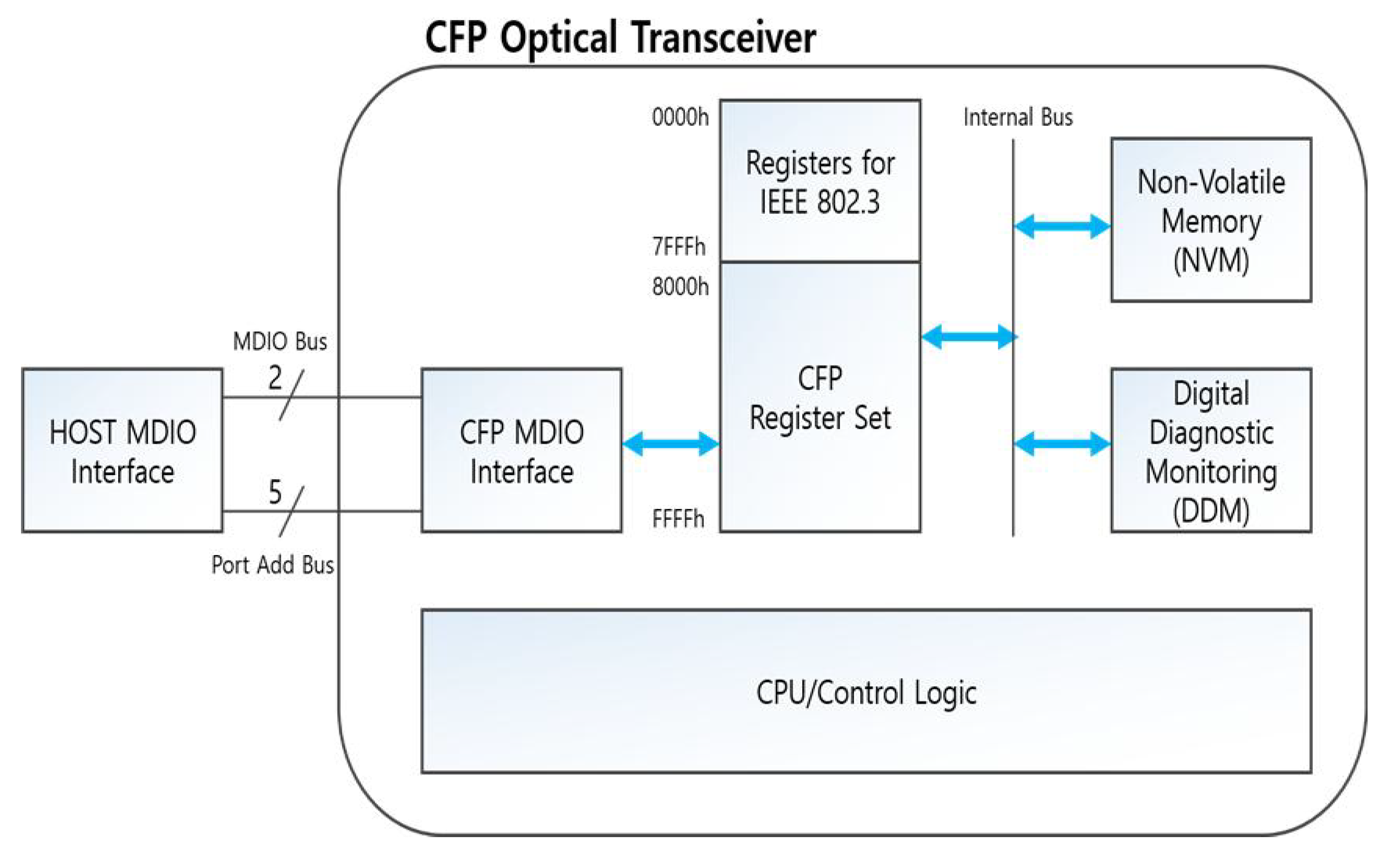
Figure 1 shows the architecture of CFP transceiver management system, which consists of three interfaces: the management data input/output (MDIO) interface between the host and CFP transceiver, the interface between the MDIO interface block and CFP register, and the interface between the CFP register, nonvolatile memory (NVM) and digital diagnostic monitoring (DDM) system. The MDIO interface is detailed in the IEEE 802.3 Clause 45 standard document [16].
2.2. CFP Register
The space of the CFP register has hexadecimal addressing ranging from 0 × 8000 to 0 × FFFF and is divided into eight sections for CFP register space allocation and access control [11]. Each section is further divided into 32 tables. Eight tables are allocated to the NVR. Tables 1, 2, 3 and 4 store basic identification (ID) information, extended ID information, network channel-specific information, and host channel-specific information, respectively. Tables 5 and 6 store information needed by the CFP manufacturer, and Tables 7 and 8 allow the user to store necessary information. Table 9 with addresses from 0 × 9000 to 0 × 9FFF is used for vendor private data. The remaining tables are assigned to the volatile register (VR) and configured to store CFP configuration, control, status, and DDM information. In implementation, CFP registers use fast memory to shadow the NVM and DDM data. The shadow registers decouple the host-side timing requirements from the internal processing, timing, and hardware control circuit-introduced latency of the module vendor.
If the vendor and user data and vendor private data are unintentionally changed, the register value of the optical transceiver may be invalid or may result in unexpected behavior. Therefore, the MSA standard recommends a password control method to limit the reading/writing of memory values in specific areas. The password is entered in CFP memory in addresses 0 × A000 and 0 × A001, with a password value of 32 bits. Through the MDIO interface, the Host enters the password value in the password entry. If the contents of both registers match the previously stored password values, the host system can read the values for the password-protected registries. If not, all values for the addresses of the protected registers will be read as 0 × FFFF.
2.3. CFP Transceiver Control and DDM
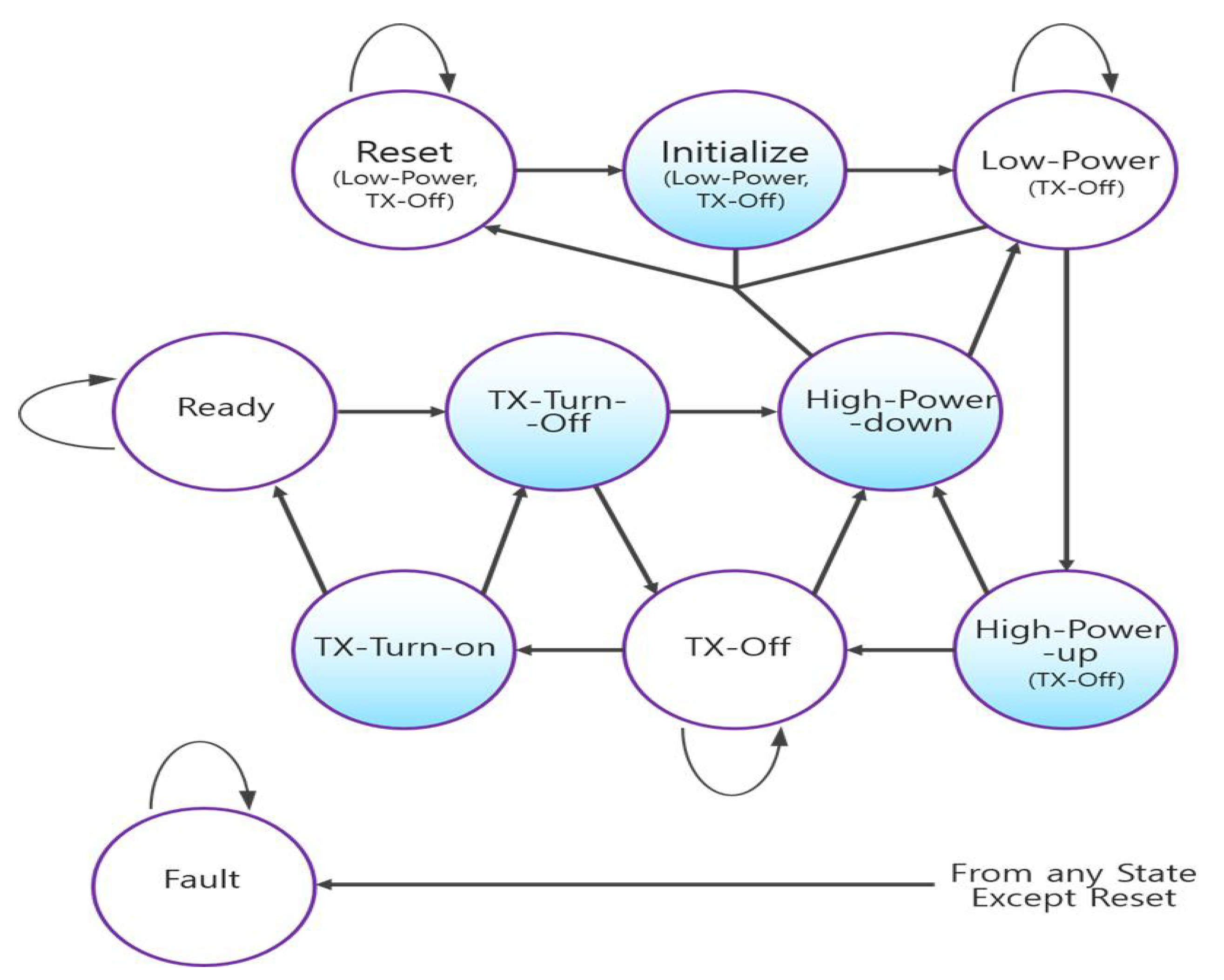
For the operation and termination of the CFP transceiver, the MSA standard defines the signals related to the CFP transceiver state transition, as shown in Figure 2. There are 10 states for initial operation, general operation, and termination. Among the 10 states, five states are transient states and five are continuous. Each state transitions to the next state when the corresponding signal is applied. Specific descriptions of these signals are omitted from this paper for brevity.
Initially, the CFP transceiver starts in a reset state, in which all circuits remain in low power mode, and transitions to the next initialization state. In this case, communication with the external host controller is disconnected and the NVR data are loaded for initial VR operation. If failure occurs, the transceiver enters a fault state or low power state. In the low power state, the CFP transceiver confirms that the MDIO interface and control circuit are ready for normal operation and enters a high power up state according to CFP state memory value and control signal. At this time, all circuits can be normally operated and stabilized, and then the tx-off state is entered. The tx-off state is the state in which the power of the optical transmitter using the network channel is not supplied. From here, the CFP transceiver can enter the tx-turn on state, in which the transceiver determines whether to use the channel according to the settings in the register. After that, the CFP transceiver finally transitions to the ready state and data are transmitted. Depending on the host request, the CFP may be in low power mode or perform a reboot. In the case of a low power mode request, it switches to the tx-off state, closes all channels, enters the high power down state, and then enters the low power state. Here, the CFP should power down all the circuitry to less than 2 Watts and keep only the MDIO interface function running. Finally, the fault state must remain in low-power mode to prevent permanent damage to the CFP, and the MDIO interface and DDM functions must be operating normal for recovery.
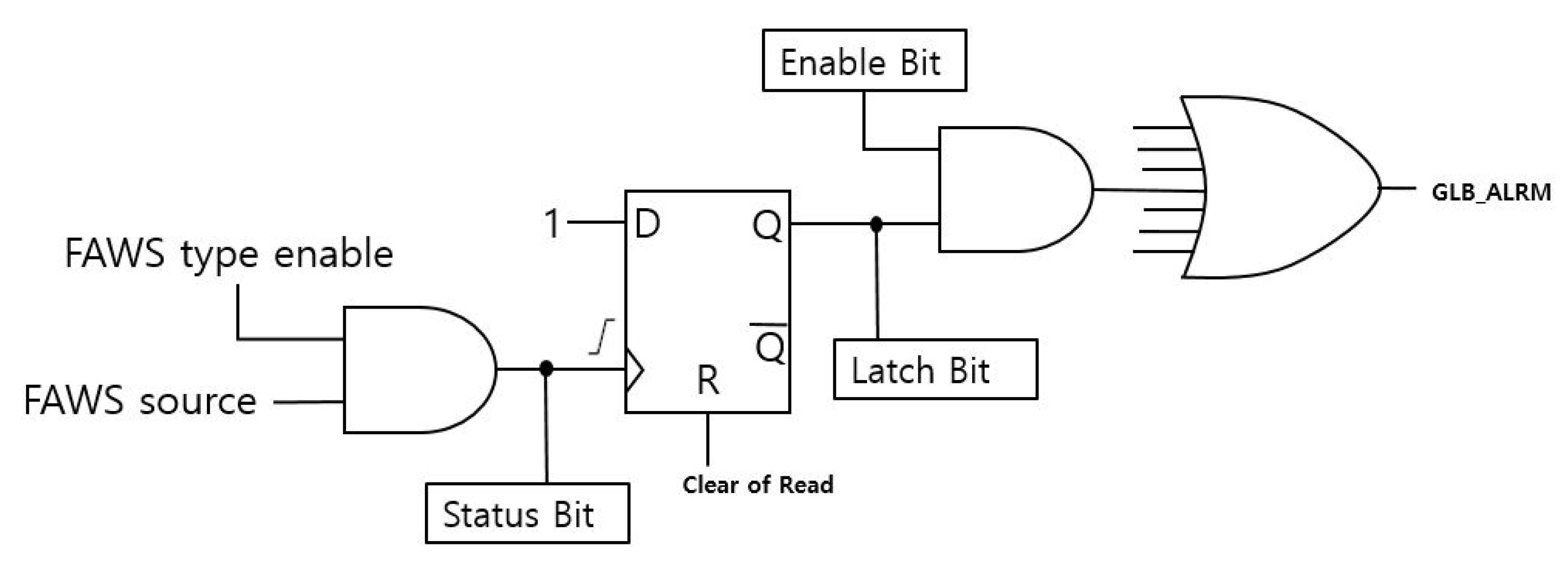
Based on the DDM information, the status of the CFP transceiver should be updated in the fault, alarm, warning, and status (FAWS) register. The Figure 3 illustrates the mechanism of the signal source contributing to the global alarm (GLB_ALRM) and the relationship among the status, latch, and enable registers. The CFP uses GLB_ALRM to alert the host about any conditions outside the normal operating conditions. In this system, the status registers drive the latch registers on a bit-by-bit basis. The logic OR of all enabled bits in the latched registers drives GLB_ALRM. When GLB_ALRM alerts the host to a latched condition, the host may query the latched registers for the condition. The latched bits are cleared from the read line of the corresponding register. Thus, a read of all latched registers can be used to clear all latched register bits and to de-assert GLB_ALRM [11].
3. CFP Firmware Design Scheme
3.1. Overall Structure Design
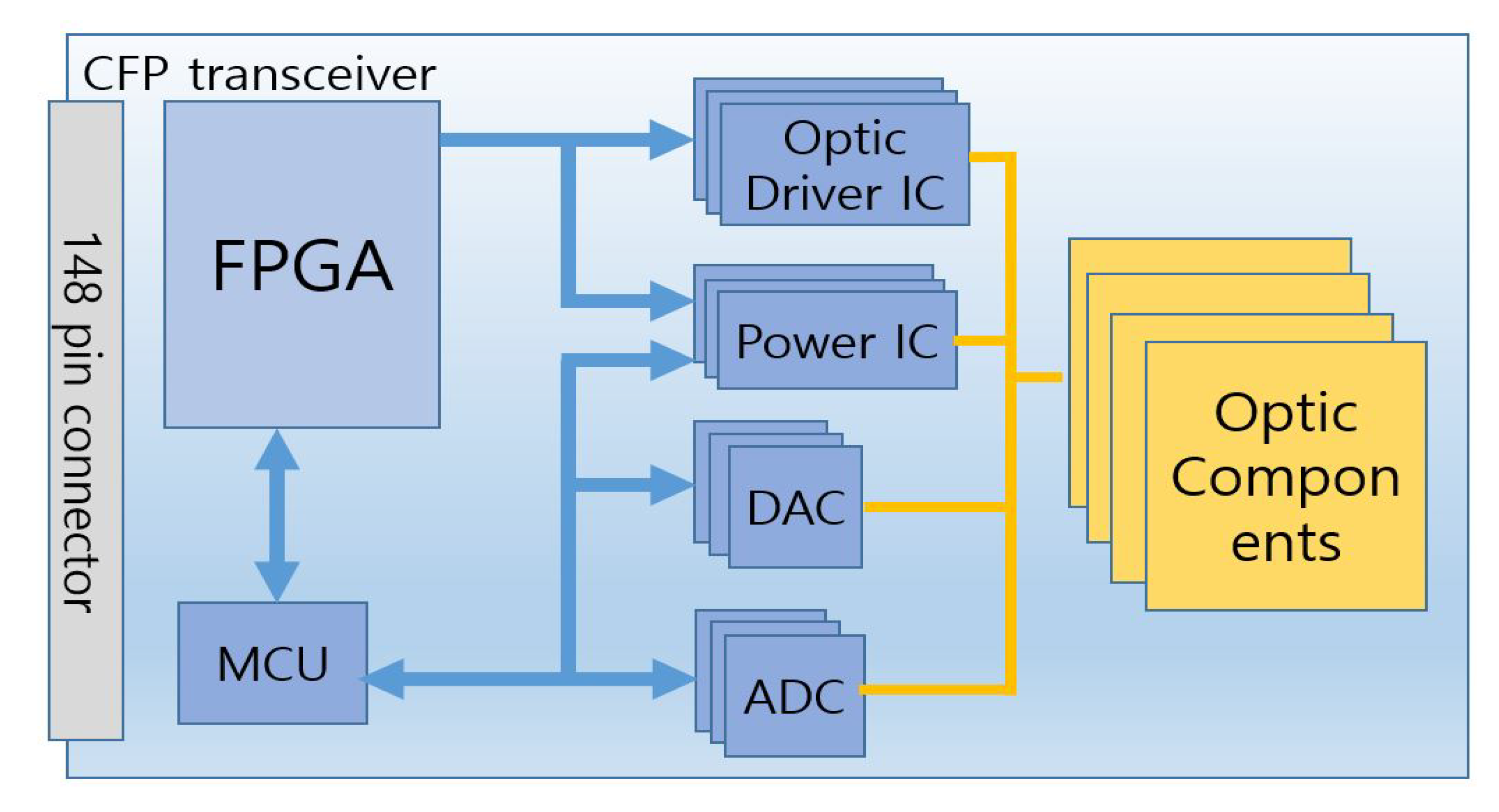
The CFP firmware is ported to the CFP hardware board for operation. Therefore, this section describes the hardware structure of the CFP used in the firmware design. Figure 4 is a block diagram of the entire hardware architecture.
In the proposed firmware design technique, an FPGA is used for the MDIO interface of the CFP and a standard memory configuration is employed. Using the FPGA, the design space is minimized by implementing multiple sub-blocks on a single chip. We also used a low-cost, reliable MCU for CFP transceiver operation and management functions. The CFP firmware must be able to control 4–16 channels. Therefore, to implement the control and monitor signals for 16 channels, it is necessary to use an MCU with large numbers of analog-to-digital converters (ADCs), digital-to-analog converters (DACs), and input/output (IO) ports for control signals. The design architecture proposed in this paper consists of external ADCs and DACs, and the MCU controls them through a communication interface to ensure channel scalability and firmware stability. In addition, ADC and DAC ICs can be selected to meet CFP transceiver performance requirements. Moreover, the IO ports for the control signals are implemented using an FPGA to relieve the burden on the MCU and achieve high speed processing.
The optic driver IC is an IC needed for the photoelectric and electronic conversion of high-speed data in the optical transceivers. The optic driver IC includes a laser driver IC that produces an optical transmission signal, a limiting amplifier IC that amplifies the signal from the optical receiver, and a clock and data recovery IC to recover the transmitted and received signals. The ICs produced by most manufacturers are controlled by a communication interface and memory map, and several optic driver ICs are required depending on the number of optical channels needed. The state signals monitored by the optical driver IC are designed to be processed at high speed through the FPGA without going through the central processing unit, because they need to be updated to the CFP standard memory quickly.
3.2. FPGA Design
The detailed functionality of CFP firmware FPGA designed in this paper consists of an MDIO interface that communicates with the host, CFP standard memory configuration and access function, CFP hardware pin control function, and CFP power control function.
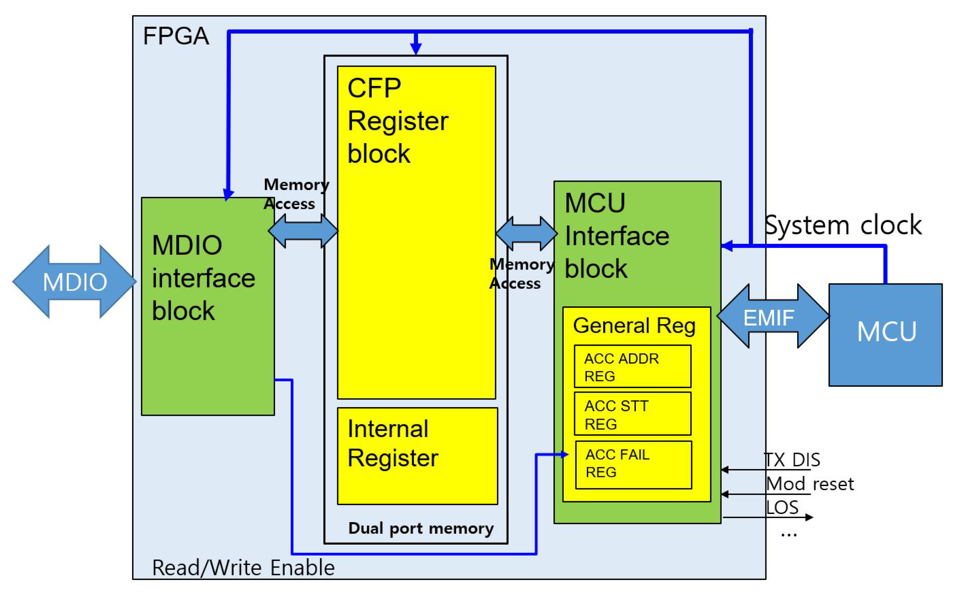
Figure 5 shows an internal functional block diagram of the FPGA. All clock sources for FPGA operation come from the MCU. The clock speed is set to 48 MHz. The driving clock is used for the MDIO interface in the FPGA that communicates with the host, the communication between the FPGA and MCU, and information transfer between the FPGA internal blocks. The MDIO interface of the FPGA is implemented to operate as an MDIO slave. It is designed to enable data access (write/read) functions according to physical addresses set by the host.
The FPGA has two main registers. The first register is the CFP register, which represents the CFP standard memory. It is implemented according to the CFP-MSA standard memory map described in Section 2, and the external host accesses the CFP register using the MDIO interface. The second register is an MCU interface register that communicates with the MCU to configure the additional memory map needed to control the CFP transceiver. The MCU monitors the access address and control request of the CFP register to the external host via the MDIO to reflect the internal CFP operation.
Table 1 describes parts of the FPGA internal register memory map. Registers 0 × 10010–0 × 10017 are CFP hardware pin-related control registers. Register 10018 is used to control the related ICs for the power supply. Register 0 × 1001B is used to limit the read/write of the specific register areas according to the password controls described in Section 2.2. When the host requests permission by entering a password value in the password entry address, the MCU controls the 0 × 1001B address of the FPGA to allow access to the register in a specific area when matched against the entered value and the previously stored password. In addition, there are CFP internal IC control-related registers, but only some of them are described due to space limitations.
The MCU interface block connects the FPGA and MCU, and MCU requests are processed through this interface block. An additional general register is implemented so that the MCU can monitor the MDIO access information and MDIO interface status.
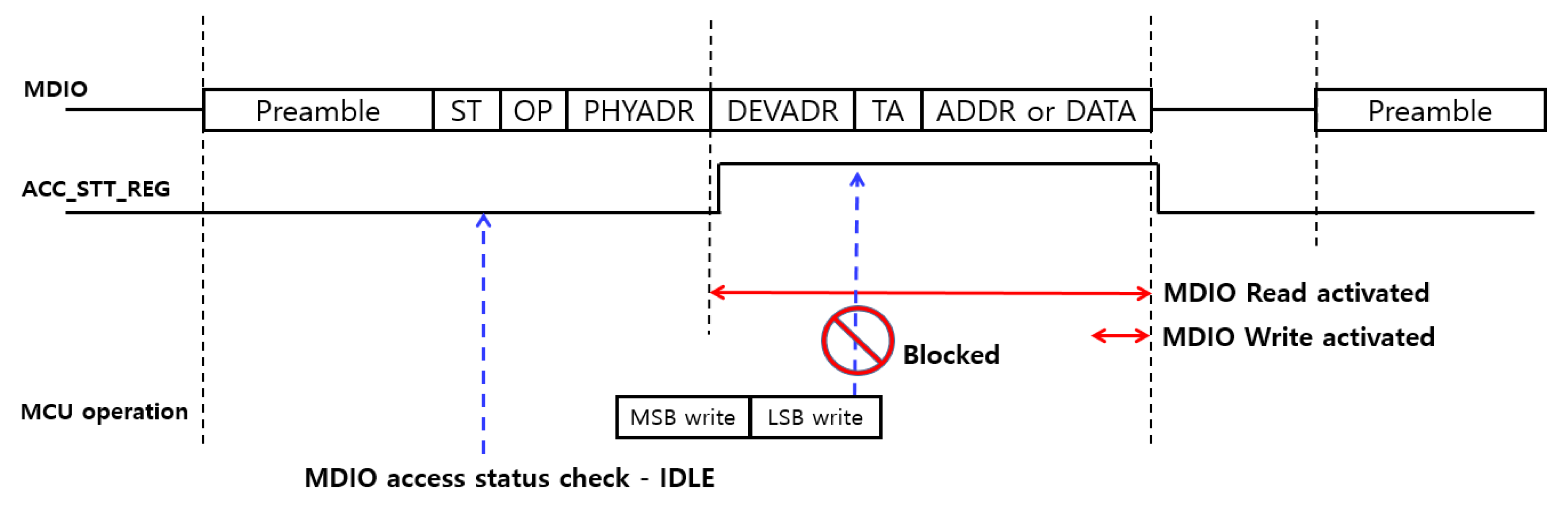
For memory read/write management, shadow memory is implemented in the FPGA using dual port memory for the CFP register area. Dual port memory is a structure that has read/write access from one of two ports. Because of this structure, if it is accessed from both sides simultaneously, invalid values may be used in memory and read. To solve this problem, priority is given to the host interface side. In other words, the MCU must not access the CFP register during the host access interval. The MCU as an internal controller should not be accessed while the host is accessing. The MCU monitors the access status register at 0 × 10060–0 × 10062 to verify that the address of the CFP register it wants to access is BUSY with the host. If the status is idle, the MCU performs the operation. However, the problem still exists. If the MCU performs the operation after verifying that the status of the access status register is IDLE, a collision occurs if the host approaches. If access is attempted by the host while the MCU is in write access, the FPGA forcibly blocks the write access of the MCU and sends the information to the MCU using register 0 × 10062. Therefore, the MCU is able to confirm whether the current operation has been completed. Figure 6 shows the timing diagram of the collision and the blocking action.
The ACC_STT_REG(access status register) signal can be found through FPGA register 0 × 10061. The MCU verifies that the status of the ACC_STT_REG signal is IDLE and then performs a write operation. When the memory write operation of the MCU is performed, the ACC_STT_REG signal is enabled after the access is recognized by the MDIO frame. Since the ACC_STT_REG signal is enabled, the write operation is blocked in the FPGA. The WR_FAIL bit at 0 × 10062 is activated. However, read operation of the MCU is allowed.
3.3. MCU Design
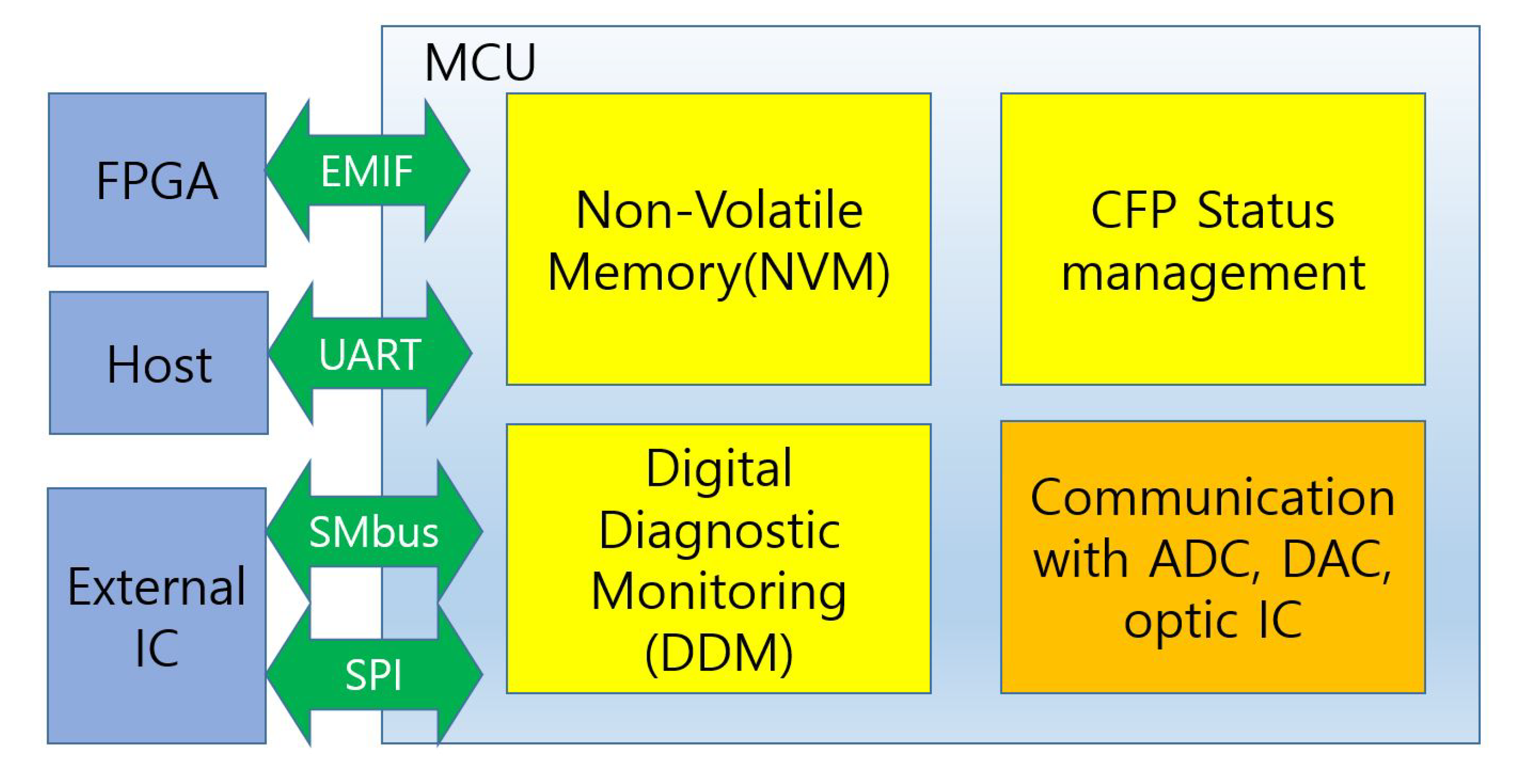
For the MCU of the CFP, 8051 Silicon Labs chips were selected. These chips are widely available in the industrial sector and provide a reliable library. They incorporate serial peripheral interface (SPI), external memory interface (EMIF), universal asynchronous receiver/transmitter (UART) and system management bus (SMbus) components for communication with external chips and support up to 256 kB of flash memory. There are various models depending on the functions to be used. To design the CFP firmware, the MCU model can be determined by considering the cost and the necessary components. It is also possible to use a different type of MCU that providing the necessary components in this paper. Figure 7 shows the internal functional block diagram and external interface of the proposed MCU.
3.3.1. NVM Function
The CFP has NVM (or nonvolatile register(NVR)) that consists of areas such as “CFP NVR”, “VENDOR NVR”, and “USER NVR”. A part of the flash memory of the MCU is allocated for the NVR memory, and the value is stored. When the CFP is powered on and initialized, the MCU implements the flash memory area value to be uploaded to the CFP register of the FPGA. The additional “VENDOR PRIVATE NVR” area is a space that can be used arbitrarily by the CFP manufacturer according to the design. In the proposed firmware design technique, the “VENDOR PRIVATE” space is used to store settings for CFP optical component performance optimization, correction values for DDM accuracy, and nonvolatile values required for other program operations.
3.3.2. DDM Function
The DDM function monitors the state of the CFP optical component read from the external ADC chip and the hardware status read by the MCU internal sensor. The values read through the external ADC are the transmit/receive optical power, transmit bias current, and transmit optical component temperature for each channel. The internal MCU sensor values are temperature and voltage. The MCU updates the monitored values from the ADC in the corresponding memory and converts the values into unit values defined in the standard document. In particular, to increase the accuracy of the transmitted and received optical power of the DDM without deviating from the standard error range, the MCU is designed to calculate the DDM value using a higher-order polynomial. The Equation (1) is DDM equation representing the received optic power.
Here is the received optical power DDM value for channel i and is the nth-order coefficient value, and calculations are performed up to the mth order. The maximum value of m is 4. A is the value monitored from the ADC, C is the value of coefficient of each term and Offset represents the offset of each channel. All coefficient values and offsets can be assigned to the CFP VENDOR PRIVATE memory, and the coefficients and offsets of each order can be set to values in floating point format (IEEE 754). In addition, the DDM value is corrected using a look-up table (LUT) to reduce the DDM error caused by the ambient temperature. The LUT value is stored in the MCU’s flash memory. Values stored in flash memory are copied to the CFP VENDOR PRIVATE memory during the optical transceiver initialization. The optical component for CFP transceiver requires a DDM calibration procedure according to temperature, as the properties of optical component vary slightly depending on the environmental temperature. The proposed method is to store the temperature-dependent calibration values in the LUT and reflect them in the final DDM value. TempCal(i) is the temperature calibration value of channel i according to the temperature. TempCal is obtained from LUT. For receiver, the final received optical power DDM value is obtained by adding the calibration value to RXPWR. The transmitter optical power DDM vaule also used the same DDM method.
Detecting the property change of the optical component by aging in the firmware itself is difficult. Therefore, DDM-related parameters are determined by sufficient age testing and precise measurements.
3.3.3. CFP Status Management Function
The CFP status management function operates the module according to the CFP state transition described in Section 2. The state transition function operates according to the control command requested from the host and the control set at the host hardware pin.
3.3.4. IC Communication Interface Function
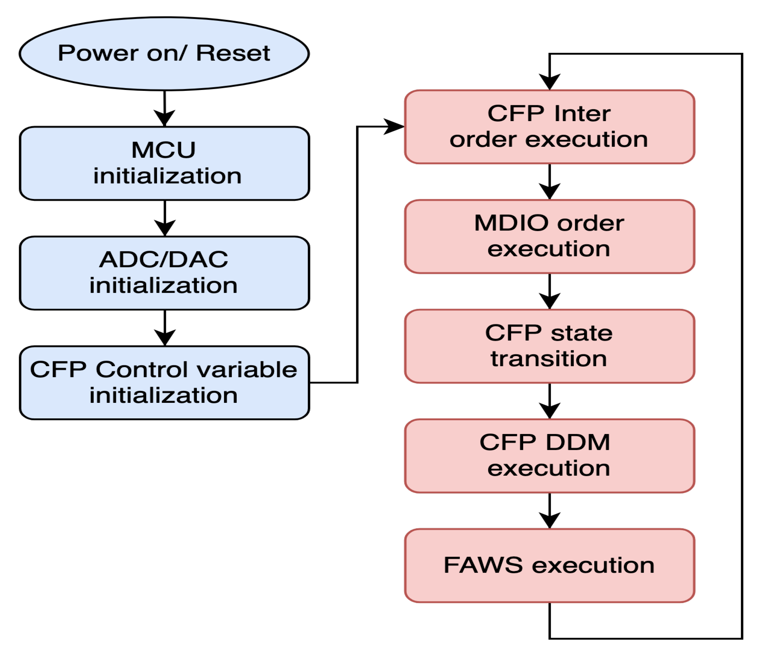
The IC communication interface function drives communication between the MCU and external chip. The MCU controls the ADCs, DACs, FPGA and optical component ICs. Table 2 describes the communication interface between the peripheral ICs and MCU. Between the FPGA and MCU, an 8051 EMIF is used for high-speed data processing. EMIF is a bus protocol for communication with external memory devices on circuit boards in integrated circuits. In this paper, the MCU considers the FPGA to be the external memory because CFP standard memory is implemented in the FPGA, as shown Figure 5. Using the address bus, data bus, RD (read), WR (write), and address latch enable (ALE), the 8051 MCU accesses the memory of the FPGA. The ADCs and DACs communicate with MCU through the SPI embedded in the chip. Moreover, optical driver ICs communicate with the MCU via the SMbus interface. UART communication between the host and MCU is implemented using the vendor IO pin of the CFP 148 pin connector, so that debugging and CFP value settings can be done easily. Figure 8 shows the MCU program flow chart. When power is supplied by default or an external reset signal is input, the MCU starts program execution. First, the MCU initializes the MCU system clock setting and MCU peripheral devices such as the EMIF, SMbus, SPI, UART, and timer. At this time, the system clock starts the FPGA.
The ADC/DAC initialization process initializes the external ADC/DAC chip. When initializing the CFP control variables, all the global variables required for the firmware are initialized and the firmware enters the polling loop. Within the polling loop, the CFP handles external requests coming into the UART. In the MDIO instruction process, the MCU accesses the internal status register of the FPGA and checks whether there is an MDIO request from the current host. If there is a request, the MCU reads the corresponding address and value and processes it accordingly. In the CFP state process, the state transition is managed as in the MSA standard. The CFP DDM process monitors the value from the ADC and updates the DDM value in the CFP standard register. The FAWS process is used to indicate faults, alarms, and warning conditions according to the CFP status.
4. Evaluation and Result
4.1. Testbed Setup
4.1.1. Optical Transceiver Testbed
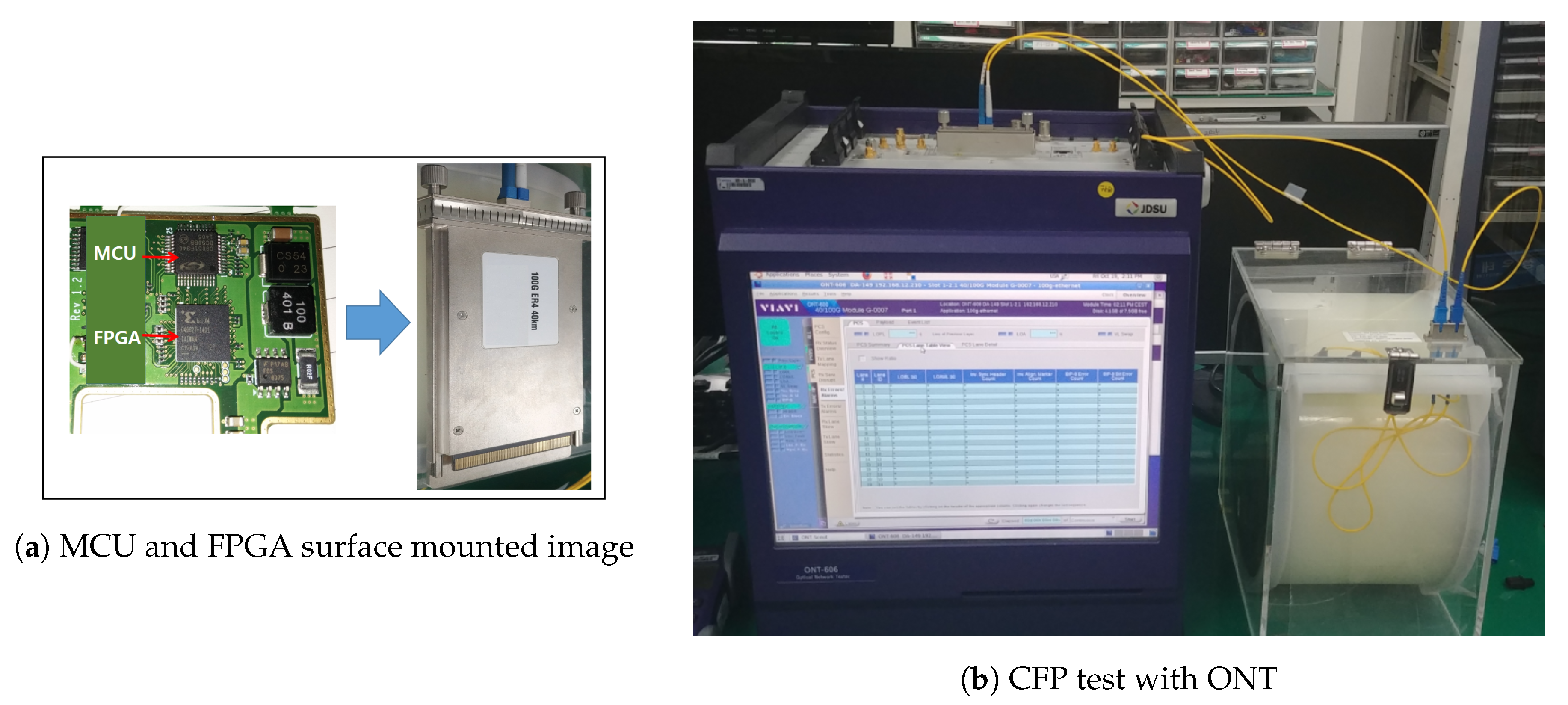
We used a Xilinx Spartan-6 series FPGA, and the MCU ported firmware was implemented using the C8051F58x series. The FPGA and MCU were surface-mounted on the PCB board as shown in Figure 9a. The PCB was assembled together with the optical components in the CFP-type case. Figure 9 shows the CFP testbed configuration. The ONT (Optical Network Tester)-606 optical network test device implemented a CFP-type optical transceiver to transmit actual data up to 100 Gbps. It could test from the Physical (PHY) layer to the Medium Access Control (MAC) layer [17]. The ONT equipment supports the insertion port of the CFP. It can perform functional tests to check whether the optical transceiver operates follows the standard and subsequentily verifies the performance of the optical transceiver. Finally, the CFP with implemented firmware was mounted on ONT-606 (VIAVI), and a self-loopback was performed using a 40 km optical cable. The hardware testbed components for firmware testing are summarized in Table 3.
Through testing, we evaluated whether the firmware could run the CFP hardware reliably and operate in compliance with the standard. Moreover, for the performance test of the proposed firmware technique, the throughput was calculated by transmitting the upper data through the CFP, and a reliability test was performed for safety confirmation. The DDM accuracy was also compared by measuring the DDM values of the implemented CFP and the existing commercial CFP products.
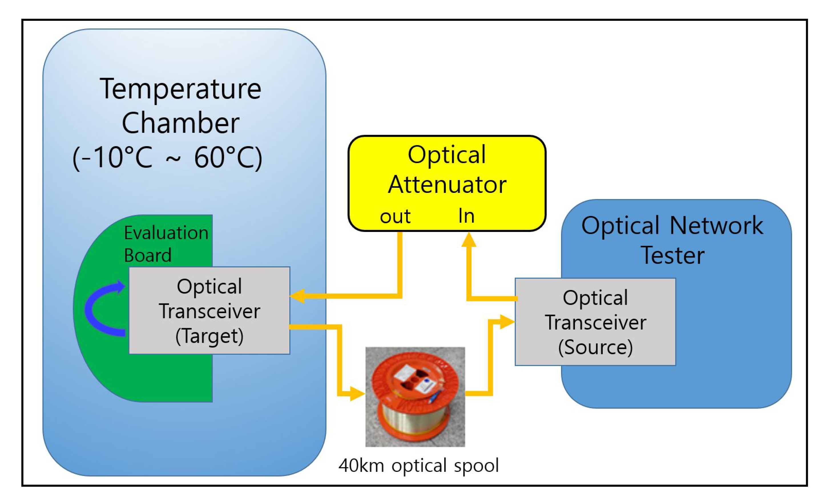
4.1.2. Temperature Testbed
Figure 10 shows a testbed configuration to test the proposed DDM temperature calibration method. A temperature chamber was used for temperature testing. The test temperature is −10° to 60° based on the chamber setting temperature. The target optical transceiver to the test is mounted on an evaluation board and placed in the chamber. The evaluation board supports the MDIO interface to read the memory information of the CFP optical transceiver and obtain the DDM value. Insert the source optical transceiver into the ONT to conduct the test outside the chamber. The source optical transceiver transmits an optical signal containing data to the target optical transceiver. The optical output of the optical transceiver inserted in the ONT equipment passes through the optical attenuator and into the input of the target optical transceiver. The optical attenuator was used to adjust the optical input power. The recommended optical transceiver operating temperature in the standard is 0° to 70°.The operating temperature criterion is the case temperature of the optical transceiver. The chamber temperature was set to −10° so that the temperature of the optical transceiver was 2°, and the chamber temperature was set to 60° to make the temperature of the optical transceiver 70°.
4.2. Results
4.2.1. Functional Test Result
The results for the CFP register memory map, transmitted/received optical power during CFP operation, alarm operation according to the received optical power, data throughput for transmission/reception, and DDM accuracy are presented in this section.
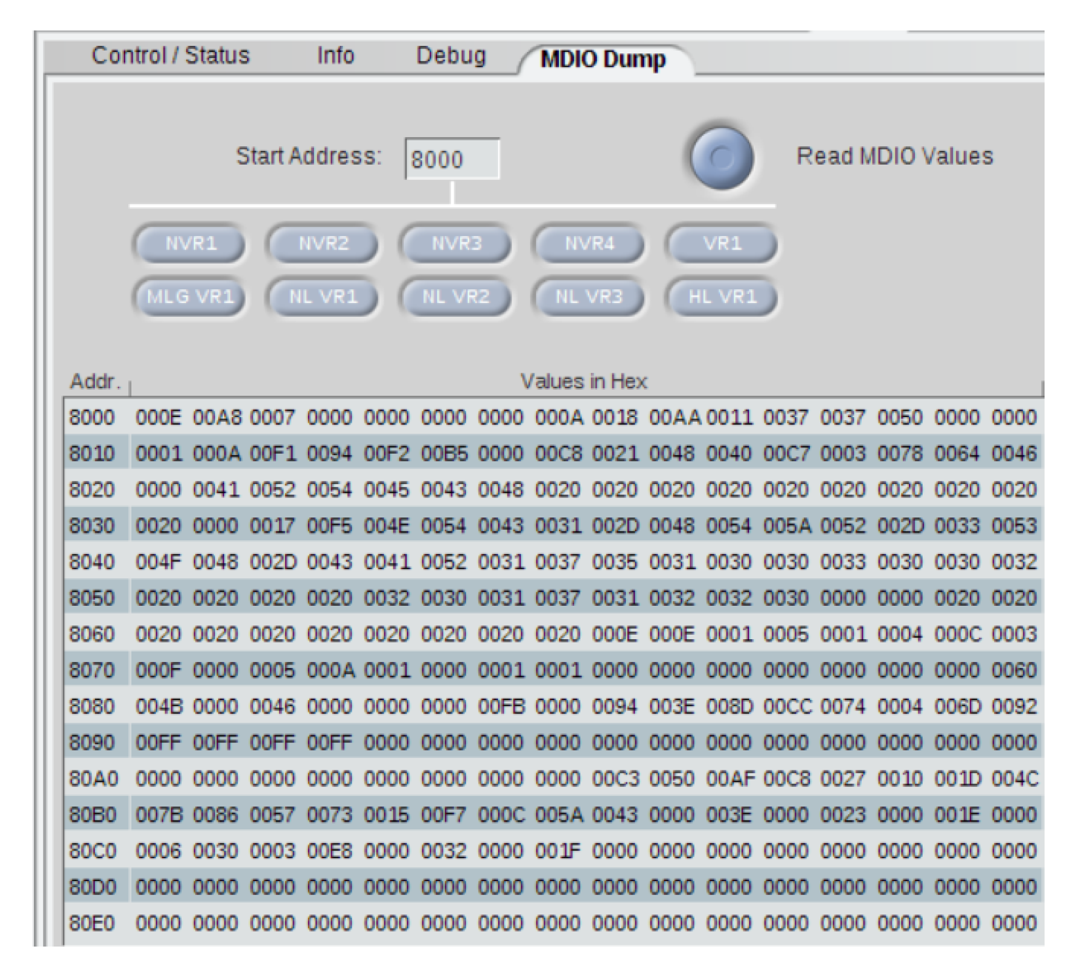
Figure 11 shows the values read from the FPGA-based CFP memory map. The addresses range from 0 × 8000 to 0 × 80FF. This result shows that the MDIO interface within the FPGA block worked normally in slave mode. Moreover, the MDIO writing function of ONT equipment confirmed that the desired value could be successfully written to the CFP standard memory.
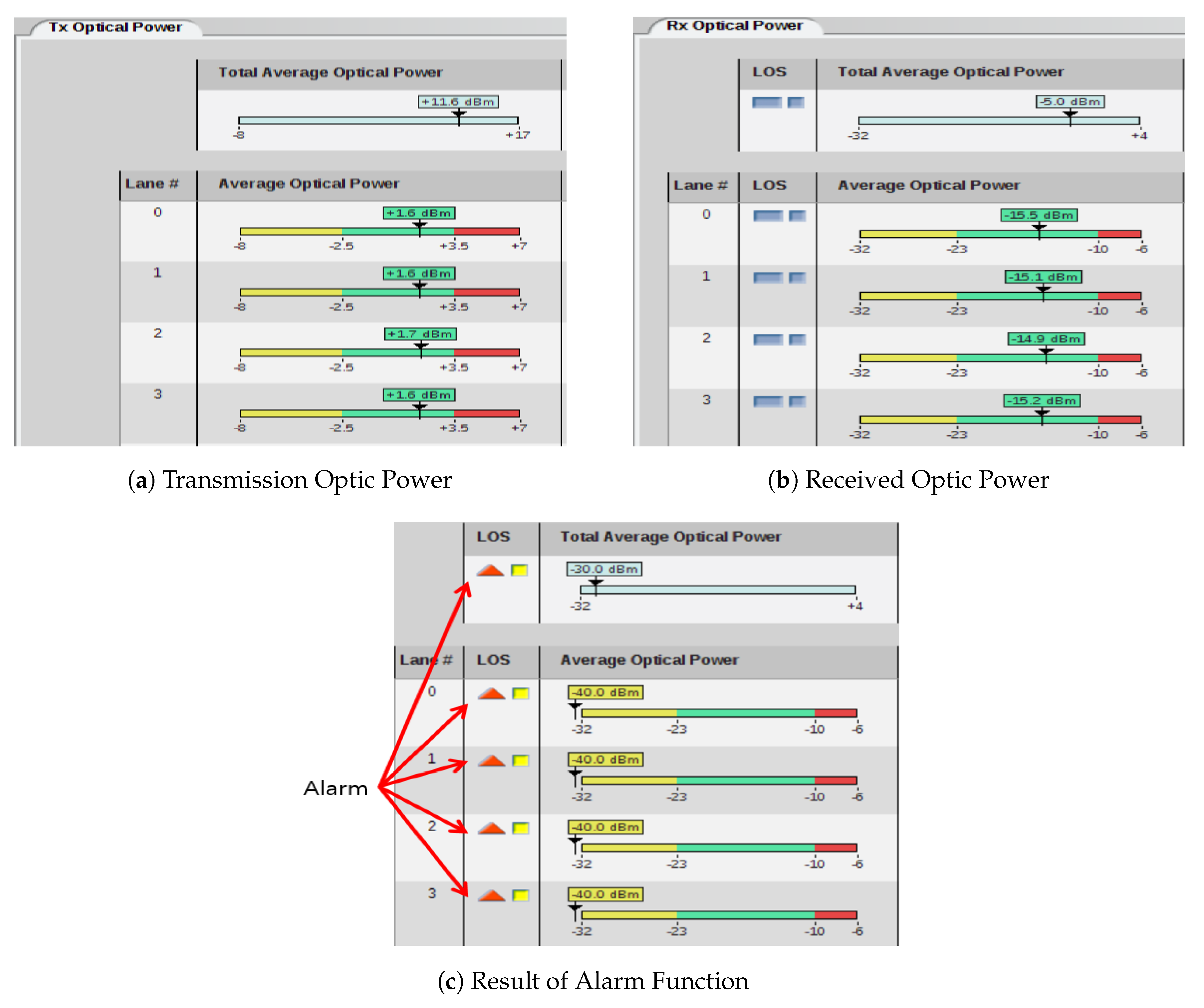
Figure 12a,b show the transmitted and received optical power values, respectively, which are within an acceptable error range (+/−2 dB). This is the result output by the DDM function proposed in Section 3. In addition, we confirmed that the temperature, CFP transceiver voltage, and DDM values of the optical components characteristics were monitored normally. Figure 12c shows the results of blocking the optical input of the receiver to check whether the alarm was displayed according to the requirements of the standard. The received optical power was found to be −40 dBm, and the loss of signal was displayed accordingly. We also confirmed that GLB_ALRM was operating normally following the implementation of the FAWS mechanism in Section 2.
4.2.2. Performance Test Result
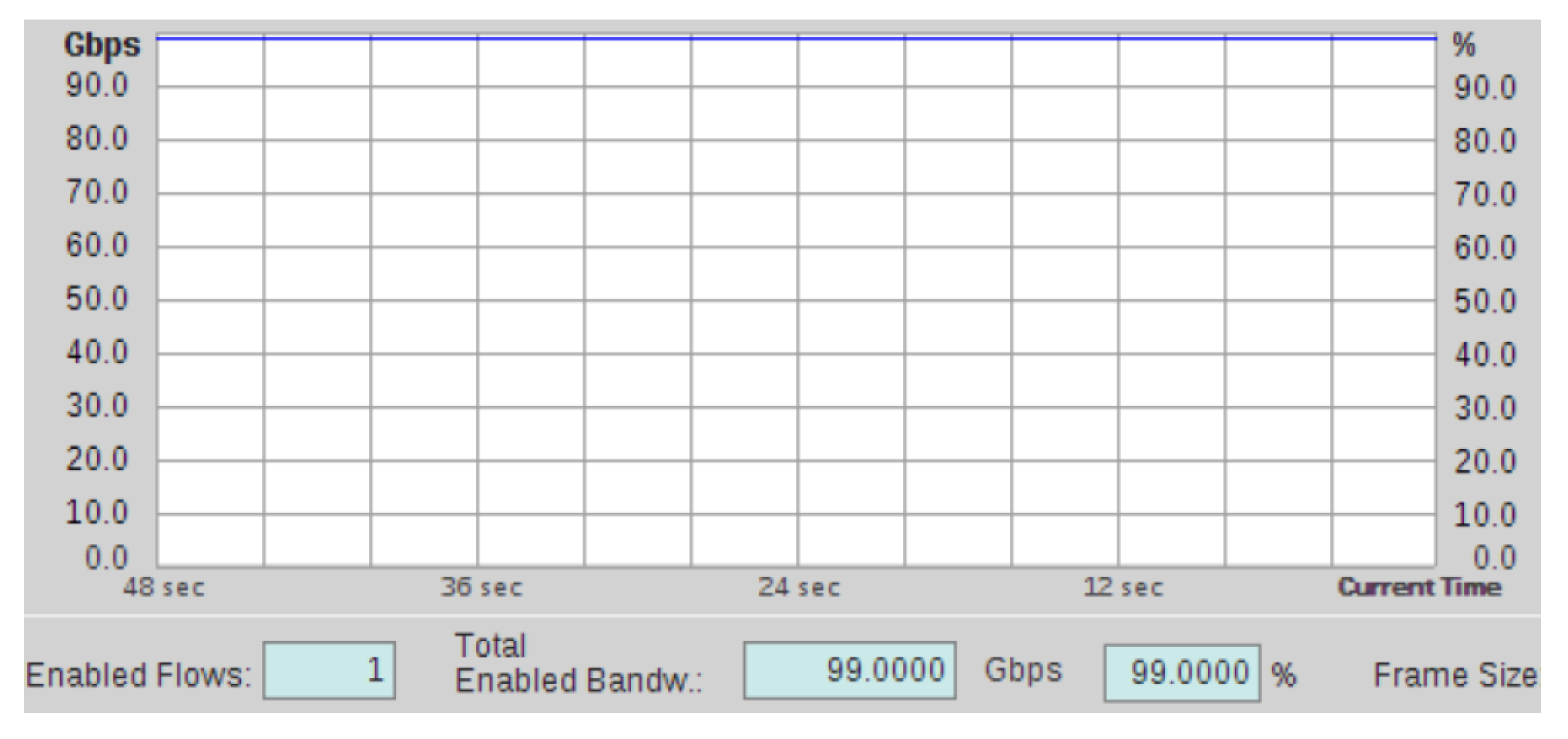
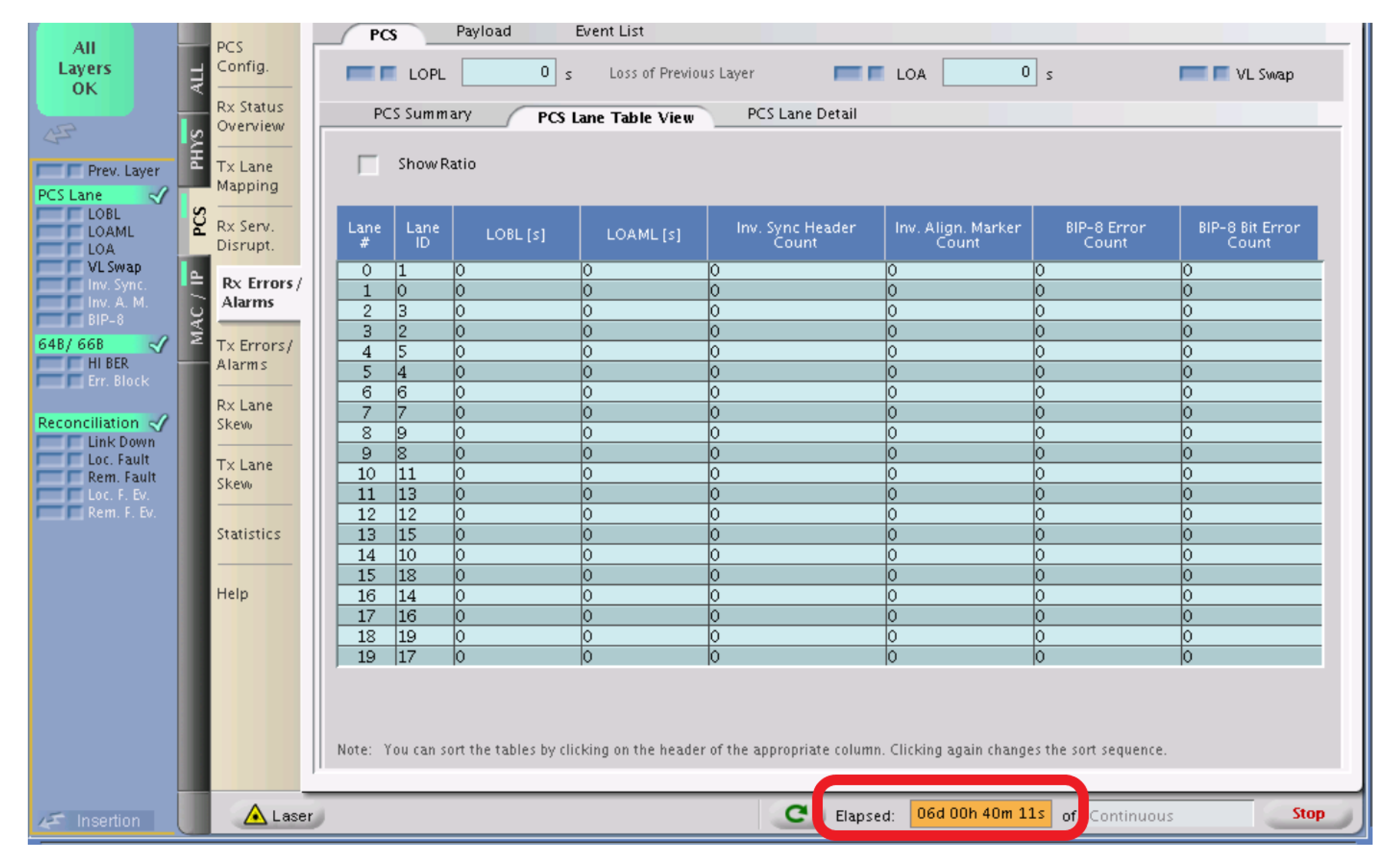
Figure 13 shows the results for the data throughput through the CFP test bed. The CFP transceiver was loaded to transmit and receive 99% of the available bandwidth. The test results confirmed that the data were transmitted and received without error at a utilization of more than 99%. Figure 14 shows the results of a long-term test for the safety and reliability of optical transceivers produced by the proposed firmware technique. It was verified that the operation was stable for more than 144 h without errors.
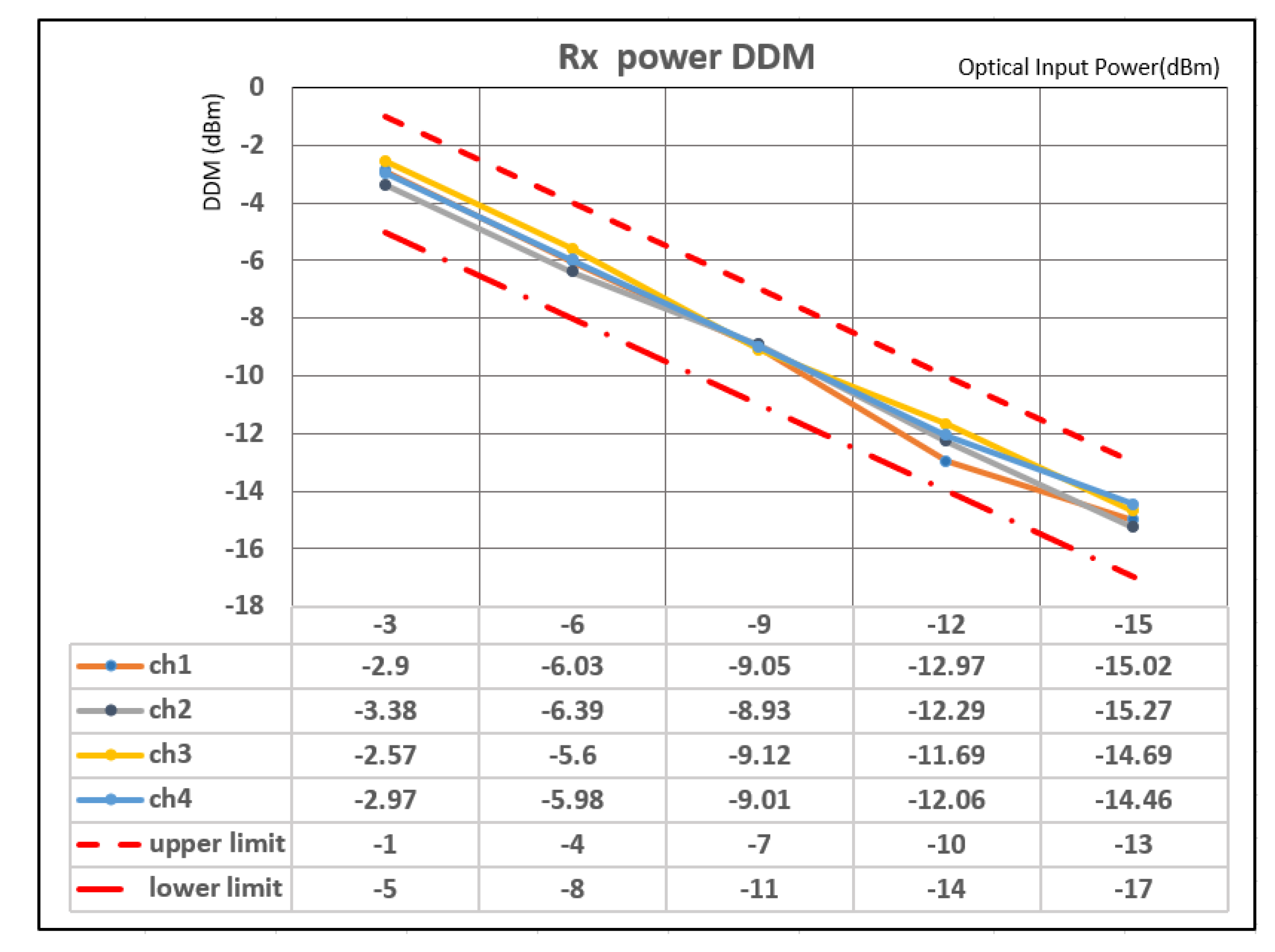
To verify the performance of the DDM function, we measured the received optical power DDM of the CFP transceiver for each channel. By adjusting the optical power input into the CFP transceiver using a variable attenuator, the received optical power DDM accuracy was measured over several sections. Figure 15 shows the received optical power DDM value of each channel measured for input optical powers ranging from −3 dBm to −15 dBm. All channels are within the margin of error, and channel 4 has the highest accuracy of 93.4%. By section, the accuracy is the highest when the optical power of −9 dBm is received. The accuracy trend varies depending on the characteristics of the optical component.
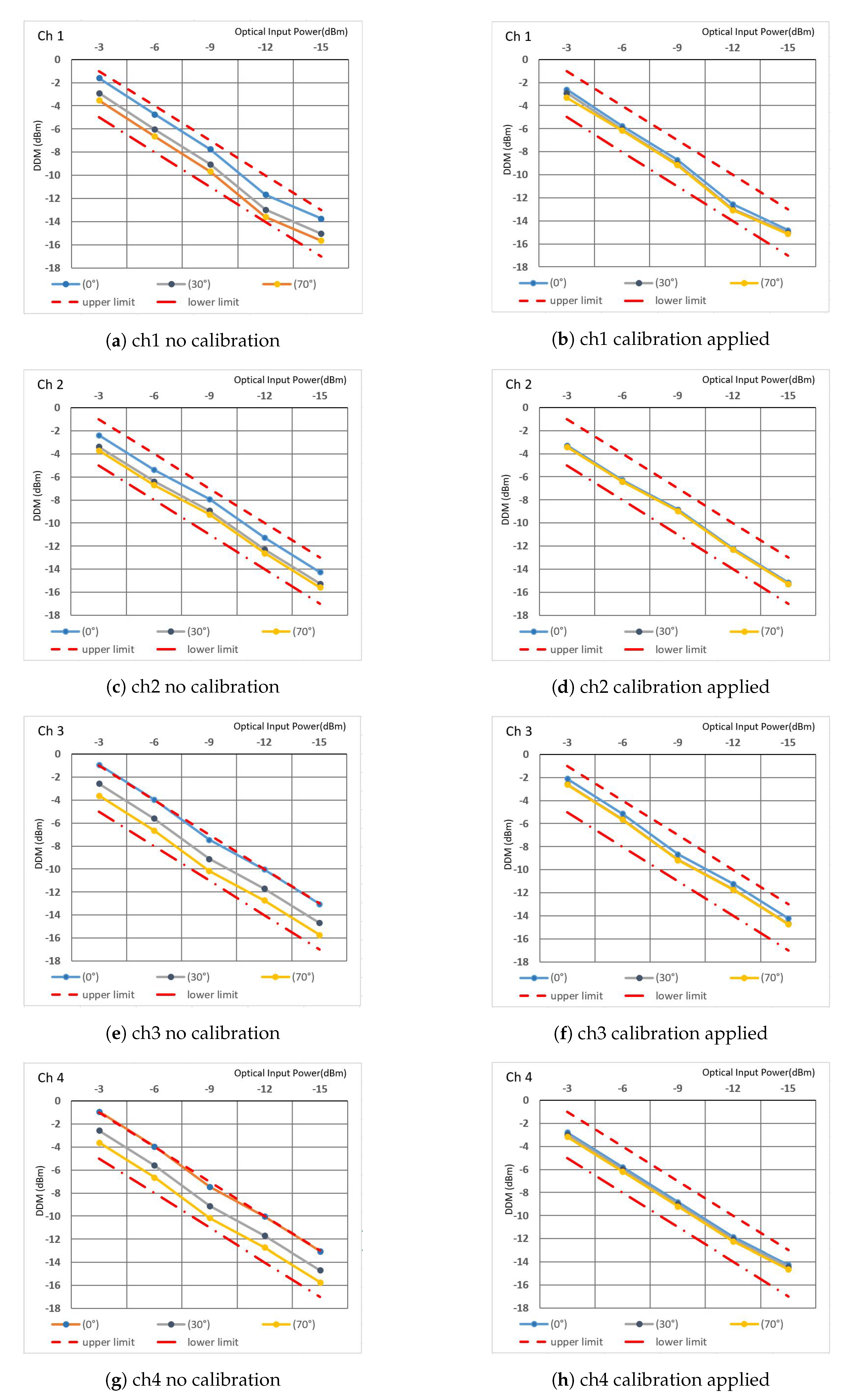
Figure 16 shows a measurement graph of the received optical power DDM before (a,c,e,g) and after (b,d,f,h) the temperature calibration at high temperature and low temperature. The measurement indicates that the DDM value is reading lower and lower as the temperature goes from low to high. Therefore, the accuracy of DDM becomes lower when it is in low temperature and high temperature environment. For channels 3 and 4, the low temperature DDM value before temperature calibration is close at the upper limit of the error range. However, the graphs of the results of applying the temperature calibration method proposed in this paper all have sufficient margins in the margin of error. This result is show that the application of the temperature calibration method proposed in this paper can maintain high DDM accuracy even in the change of optical component properties with temperature.
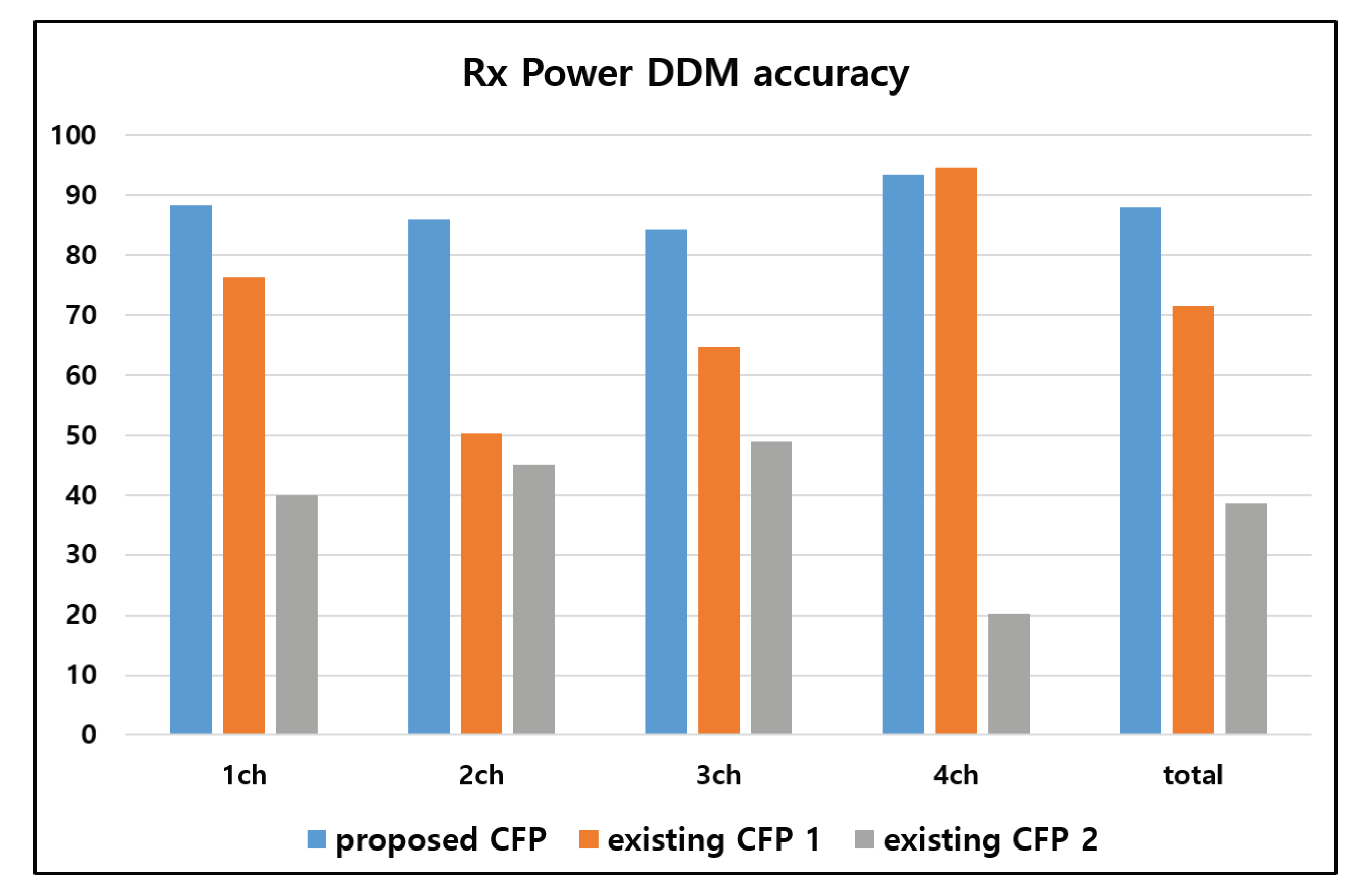
Figure 17 shows the received optical power DDM accuracy of the proposed firmware and a conventional commercial CFP transceiver. Unfortunately, the methods for calculating DDM in existing CFP are not disclosed, so technical differences cannot be compared, but they can be compared by measuring DDM accuracy. The results show that the DDM accuracy of an existing CFP product is higher than that of the proposed scheme in some channels, but the accuracy in all channels with the proposed method is higher than that of an existing CFP transceiver. Moreover, the results confirm that the deviation of the DDM accuracy among the channels in the proposed firmware is less than that resulting from the conventional method.
Finally, the advantages of the proposed firmware design are summarized in Table 4. The proposed technique allows up to 16 channels to be expanded using the FPGA and can flexibly expand external chips depending on the required functions. The external ADC/DAC chips are used, and communication interfaces are implemented, if high-end ADC/DAC chips are required, external chips can be changed without MCU replacement. Furthermore, the implementation of the CFP standard memory in the FPGA is hardware separated from the MCU. This method can ensure the optical transceiver stability by being managed by the FPGA to allow access to the CFP standard memory from outside, even if there is a temporary problem with MCU operation. Our proposed method also used vendor IOport (Vendor IOport) on CFP standard connectors to help update the FPGA and MCU, and to allocate serial interfaces to debug the optical transceiver.
5. Conclusions
In this paper, we proposed a 100 Gbps CFP firmware design based on the MSA standard and verified its utility by evaluating the actual implemented firmware in a testbed. In the proposed method, the communication interface is implemented using an external host and the internal operations of the CFP are performed using an FPGA and MCU, and it was ported to actual CFP hardware. The validity of the proposed firmware design technique was verified through the correct operation of the CFP transceiver according to the MSA operation management standard. Moreover, we proposed a method of calculating DDM considering temperature and high accuracy. the testbed results confirmed that the DDM accuracy is excellent, based on comparison of the performance of the proposed firmware with that of the CFP transceiver of an existing product. This paper also proposed memory design and memory access technic for stable memory access and operation of optical transceiver and confirmed safety through testing.
The proposed technique can also be used for CFP-type optical transceivers such as CFP2 or CFP4. The overall bandwidth of the optical transceiver depends on the number of optical components or channels being used. This approach was designed considering the expandability of channel so that it can be applied to the development of 200/400 Gbps CFP-type modules such as CFP8 in the future. Applying the techniques proposed for high-bandwidth CFP types requires only specific modifications according to optical components and optical driver ICs.
The proposed firmware method satisfies the requirements of the standard but does not consider optional conditions such as firmware remote update. The MSA standard document describes the mutual procedure between the host system and the optical transceiver for the remote firmware update of the optical transceiver. The host systems using optical transceivers should support to send commands according to standard procedures for remote downloads. Therefore, in future research, the remote firmware download procedure will be tested by implementing not only optical transceiver but also host-side functions following standards. In addition, various data driver ICs are being released as the data transfer rate is increasing to 200/400 Gbps. We therefore plan to design and implement the interface driver accordingly.
Author Contributions
Design and Implementation J.-W.K.; formal analysis S.-H.K.; hardware S.-M.S.; writing—review and editing D.-S.K. All authors have read and agreed to the published version of the manuscript.
Funding
This research was supported by Basic Science Research Program and Priority Research Centers through the National Research Foundation of Korea (NRF) funded by the Ministry of Education (2019R1I1A1A01063895, 2018R1A6A1A03024003).
Acknowledgments
The author would like to thank the Co. ARTECH for the the data provided.
Conflicts of Interest
The authors declare no conflict of interest.
References
- Agiwal, M.; Roy, A.; Saxena, N. Next Generation 5G Wireles Networks: A Comprehensive Survey. IEEE Commun. Surv. Tutor. 2016, 18, 1617–1655. [Google Scholar] [CrossRef]
- Lee, J.J.; Heo, J.Y.; Gang, S.G.; Lee, J.K.; Lee, J.C.; Lee, D.S. Market and Technology Trends in 100Gb/s Optical Transceiver. Electron. Telecommun. Trends 2015, 30, 65–76. [Google Scholar]
- Myeong, S.I.; Lee, J.C.; Gang, H.S.; Lee, J.H. Development of embedded optical transceiver technology for real-time Optical Time Domain Reflectometer(OTDR) function. J. Inst. Electr. Inf. Eng. 2015, 42, 103–106. [Google Scholar]
- Lee, J.H.; Seo, C.U.; Na, S.D.; Do, H.T. Small Cap Hot Issue-Optical Communication and Bright Stock. Available online: https://www.sks.co.kr/main/lucene/search/index.cmd (accessed on 29 January 2020).
- Adballan, W.; Krichen, D.; Boudriga, N. An optical backhaul solution for LiFi-based access networks. Opt. Commun. 2020, 454, 124473. [Google Scholar]
- Yang, S.J.; Yeon, J.W.; Lee, H.H. High-Performance Low-Complexity Iterative BCH Decoder Architecture for 100Gb/s Optical Communications. IEIE J. 2013, 50, 140–148. [Google Scholar] [CrossRef] [Green Version]
- Aruga, H.; Mochizuki, K.; Itamoto, H.; Takemura, R.; Yamagishi, K.; Nakaji, M.; Sugitatsu, A. Four-channel 25Gbps optical receiver for 100Gbps Ethernet with built-in demultiplexer optics. In Proceedings of the 36th European Conference on Optical Communication, Torino, Italy, 19–23 September 2010. [Google Scholar]
- Cole, C. 100-Gb/s and beyond Ethernet optical interfaces. In Proceedings of the OptoElectronics and Communications Conference 2010 Technical Digest, Sapporo, Japan, 5–9 July 2010. [Google Scholar]
- Doi, Y.; Ohyama, T.; Yoshimatsu, T.; Soma, S.; Oguma, M. 400GbE demonstration utilizing 100Gbe optical sub-assemblies and cyclic arrayed waveguide gratings. In Proceedings of the Optical Fiber Communication(OFC) 2014, San Francisco, CA, USA, 9–13 March 2014; pp. 1–3. [Google Scholar]
- IEEE 802.3 400 Gb/s Ethernet Study Group. 400G Optical Transceivers; LUXTERA: Carlsbad, CA, USA, 2013; pp. 1–26. [Google Scholar]
- CFP MSA Group. CFP MSA Management Interface Specification Version 2.6 r06a. CFP Multi-Source Agreement (CFP MSA). 2017. Available online: http://www.cfp-msa.org/Documents/CFP_MSA_MIS_V2p6r06a.pdf (accessed on 24 March 2017).
- CFP MSA Group. CFP MSA Hardware Specification Version 1.4. CFP Multi-Source Agreement (CFP MSA). 2010. Available online: http://www.cfp-msa.org/Documents/CFP_MSA_HW-Spec-rev1-40.pdf (accessed on 7 June 2010).
- Chujo, N.; Takemoto, T.; Yuji, F.; Yamashita, H. High-frequency circuit design for 25Gb/s × 4 optical transceiver. In Proceedings of the 18th Asia and South Pacific Design Automation Conference (ASP-DAC), Yokohama, Japan, 22–25 January 2013. [Google Scholar]
- Laperle, C.; O’Sullivan, M. Advances in High-Speed DACs, ADCs, and DSP for Optical Coherent Transceivers. J. Light. Technol. 2014, 32, 629–643. [Google Scholar] [CrossRef]
- Lossio, R. PSoC 3 and PSoC 5LP—Creating a CFP Management Interface. CYPRESS. 2018, pp. 1–18. Available online: https://www.cypress.com/documentation/application-notes/an83902-psoc-3-and-psoc-5lp-creating-cfp-management-interface (accessed on 20 June 2018).
- IEEE Standard for Ethernet Working Group. IEEE 802.3ae:10 Gbit/s (1,250 MB/s) Ethernet over Fiber. 10GBASE-SR/-LR/-ER/-SW/-LW/-EW/-LX4. 2003. Available online: http://www.ieee802.org/3/ae/ (accessed on 29 January 2020).
- VIAVI Solutions. ONT-600 Optical Network Testers High-Speed Testing for High-Speed Optical Networks. 2019. Available online: https://www.viavisolutions.com/en-us/product-family/optical-network-tester-ont (accessed on 29 January 2020).
Figure 1.
C Form-Factor Pluggable (CFP) Management Interface Architecture [11].
Figure 1.
C Form-Factor Pluggable (CFP) Management Interface Architecture [11].

Figure 2.
State Transition Diagram of Optical Transceiver [11].
Figure 2.
State Transition Diagram of Optical Transceiver [11].

Figure 3.
Fault, Alarm, Warning, and Status (FAWS) Signal Model for a Single Bit [11].
Figure 3.
Fault, Alarm, Warning, and Status (FAWS) Signal Model for a Single Bit [11].

Figure 4.
CFP Optical Transceiver Block Diagram.

Figure 5.
Field Programmable Gate Array (FPGA) Block Diagram.

Figure 6.
Blocking Operation of Micro Controller Unit (MCU) Accessing.

Figure 7.
MCU Function Block Diagram.

Figure 8.
MCU Program Flow Chart.

Figure 9.
CFP Testbed Setup.

Figure 10.
Temperature Testbed Block Diagram.

Figure 11.
Access of CFP Memory Map.

Figure 12.
Results of Digital Diagnostic Monitoring (DDM) and Alarm.

Figure 13.
Throughput of the CFP Optical Transceiver.

Figure 14.
Reliability Test of the CFP Optical Transceiver.

Figure 15.
Graph of Rx power DDM.

Figure 16.
Graph of Rx Power DDM about Temperature Calibration.

Figure 17.
Graph of Rx Power DDM Accuracy Comparison.


Table 1.
FPGA Internal Register.
| Addr | Name | RW | Content |
|---|---|---|---|
| 10010 | PRTADR_REG | RW | PRTADR[4:0] Pin Strap value |
| 10012 | PRG_CNT_REG | RW | PRG_CNT_1∼3 Pin value |
| 10016 | CTRL_IN_REG | RW | TX_DIS pin, MOD_LOPWR pin, |
| MOD_RSTn pin value | |||
| 10017 | TX_DIS | RW | Tx Disable for each channel |
| 10018 | POWER_REG | RW | Internal CFP power switch |
| 1001B | PROT_REG | RW | [2]: Vendor private protect |
| [1]: User NVR protect | |||
| [0]: Vendor NVR protect | |||
| 10060 | ACC_ADDR_REG | R | [15:0] Address |
| 10061 | ACC_STT_REG | R | [1]: Read access status |
| [0]: Write access status | |||
| 10062 | ACC_STT_REG | R | [1]: Read fail |
| [0]: Write fail |
Table 2.
MCU interface.
| IC | Interface |
|---|---|
| FPGA | EMIF |
| ADC | SPI |
| DAC | SPI |
| Optic Driver IC | SMbus |
| Host | UART |
Table 3.
Testbed Setting.
| Item | Setting |
|---|---|
| FPGA | Xilinx Spartan-6 Series |
| MCU | Silab C8051F58x Series |
| DAC/ADC | MAXIM 12bit ADC/DAC |
| Optic Driver IC | Semtech 10G Driver IC |
| Board & Case | ARTECH CFP module |
| Test distance | 40Km optical spool |
| Host | VIAVI ONT (Optical Network Tester) 606 |
Table 4.
Advantages of Proposed Design.
| Advantage | Explanation |
|---|---|
| Scalability | - Flexible expansion of up to 16 channels |
| - Flexible external chip can be added | |
| Stability | - CFP memory block and operating functions |
| separated by hardware module | |
| Utility | - Easy firmware update and CFP control through vendor IO |
© 2020 by the authors. Licensee MDPI, Basel, Switzerland. This article is an open access article distributed under the terms and conditions of the Creative Commons Attribution (CC BY) license (http://creativecommons.org/licenses/by/4.0/).
Share and Cite
MDPI and ACS Style
Kim, J.-W.; Kim, D.-S.; Kim, S.-H.; Shin, S.-M. The Firmware Design and Implementation Scheme for C Form-Factor Pluggable Optical Transceiver . Appl. Sci. 2020, 10, 2143. https://doi.org/10.3390/app10062143
AMA Style
Kim J-W, Kim D-S, Kim S-H, Shin S-M. The Firmware Design and Implementation Scheme for C Form-Factor Pluggable Optical Transceiver . Applied Sciences. 2020; 10(6):2143. https://doi.org/10.3390/app10062143
Chicago/Turabian StyleKim, Jae-Woo, Dong-Seong Kim, Seung-Hwan Kim, and Sang-Moon Shin. 2020. "The Firmware Design and Implementation Scheme for C Form-Factor Pluggable Optical Transceiver " Applied Sciences 10, no. 6: 2143. https://doi.org/10.3390/app10062143
Note that from the first issue of 2016, this journal uses article numbers instead of page numbers. See further details here.