Small-Size Square Ring 1-Bit Reconfigurable Transmitarray Unit Cell for C-Band Applications


Department of Microelectronics and Radio Engineering, Saint Petersburg Electrotechnical University “LETI”, 5 Prof. Popov Str., Saint Petersburg 197376, Russia
*
Author to whom correspondence should be addressed.
Appl. Sci. 2020, 10(9), 3319; https://doi.org/10.3390/app10093319
Submission received: 22 April 2020
/
Revised: 3 May 2020
/
Accepted: 6 May 2020
/
Published: 10 May 2020
(This article belongs to the Section Electrical, Electronics and Communications Engineering)
Abstract
:The paper presents a reconfigurable linear polarized transmitarray unit cell design with 1-bit phase quantization for C-band applications. The unit-cell structure consists of two square ring patches of reduced size, which are connected using a coupling element. Incorporating p-i-n diodes inside the coupling element allows controlling the current flow direction in the antennas and providing a 180° phase difference. An analysis of the unit-cell insertion loss contributed by small-size antennas and coupling between them is discussed. The p-i-n diode parasitic parameters are taken into consideration of the unit cell performance simulation. It was shown that the insertion loss caused by the p-i-n diodes parasitic parameters can be reduced. The original biasing circuitry providing p-i-n diodes control voltage is proposed. Simulation results of the reconfigurable unit cell are validated by measurements in a waveguide. As a result of measurements, the insertion loss is −2.3 dB at 5.9 GHz, the reflection coefficient module is less than −20 dB, the phase difference error does not exceed ± 1° in the passband, while 3-dB bandwidth corresponds to 180 MHz (3.4%).
1. Introduction
Nowadays, increasing the number of users of wireless networks and speedy progress in the Internet of Things (IoT), vehicle-to-vehicle communication for autonomous and anti-collision driving leads to growing requirements to channel capacity and throughput. Millimeter-wave communication is a promising candidate in terms of bandwidth enhancement. On the other hand, such systems require high gain antennas to overcome the path losses in the millimeter-wave frequency range.
Metasurfaces [1,2], reflectarrays [3] or transmitarrays [4] can be an attractive solution. They consist of a feed antenna and periodically placed unit cells that provide the required phase distribution along the radiating aperture. Changing the phase distribution by incorporating the tuneable components inside the unit cells of the transmitarray allows obtaining the beam-steering capability. The phase states of the unit cells can be changed continuously or discretely. The continuous phase shift range is defined by the slope of the phase of the transmission coefficient. The sharp slope can be obtained by using complicated multilayer structures. The tuneable materials as ferroelectrics [5] or liquid crystals [6] usually can provide a continuous phase shift in the limited narrow frequency range due to the technological limitation with the number of layers of the structures. Additionally, the liquid crystals suffer from the complexity of realization, strong temperature dependence and low switching speed. The ferroelectrics require a high level of an applied voltage. The varactor diodes are an attractive solution for tuneable transmitarrays [7]. The wide continuous phase shift range can be obtained by using varactor diodes. The drawback is a low power capability due to the nonlinearity of characteristics and narrow bandwidth performance. The p-i-n diodes can provide the discrete phase states of the unit cell. The design of the unit cell and the number of p-i-n diodes define the number of phase states. Decreasing the number of phase states or, in other words, low-bit phase quantization leads to gain loss of the array [8]. At the same time, a 1-bit phase quantization with two phase states 0° and 180° minimizes the number of p-i-n diodes per unit cell and, in such a way, provides a low insertion loss level and avoids an array complexity. Another advantage of p-i-n diodes is the ability to operate over a wide frequency range up to a millimeter-wave [9,10]. The critical aspect of the reconfigurable unit cell design is to take into account the parasitic parameters of the p-i-n diodes and to minimize its impact on the unit cell performance.
Traditionally, a unit cell of the transmitarray consists of receiving and transmitting antennas connected through a phase shifter. Alternatively, the antennas can be coupled to each other asymmetrically, depending on the required phase shift. The interlayer connections can be implemented by aperture coupling or the plated vias [11,12]. The last one provides a more simplified way for phase switching. In a 1-bit reconfigurable unit-cell selecting the feed point by low-loss RF switches changes the current flow direction in a receiving and transmitting antennas, and thus, the required 180° phase shift is provided [13,14,15].
In this paper, the reconfigurable unit cell design for the C-band application is presented. The p-i-n diodes are used to provide electronically switching of the phase states with 180° phase difference. The unit-cell insertion loss contributed by antennas layout and coupling between them is described. Additionally, special attention is paid to decrease the influence of the p-i-n diodes parasitic parameters on the unit cell performance. The proposed unit-cell was fabricated and measured inside the waveguide-based setup. The measured results are in good agreement with full-wave electromagnetic (EM) simulations. The unit cell can be used for transmitarray design with a beam-steering capability and can be scaled from C-band to a higher frequency range.
2. Unit-Cell Design
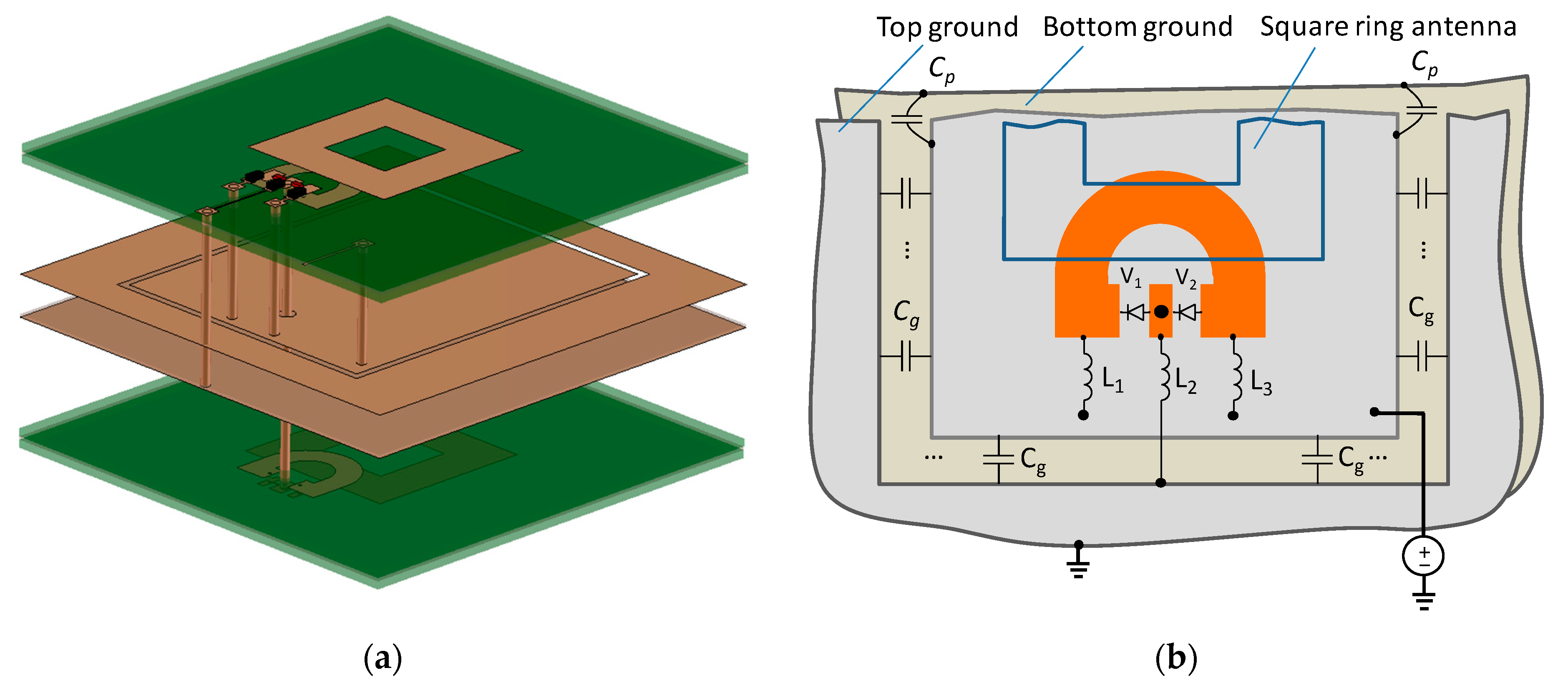
The unit cell design is represented in Figure 1a. The transmitarray unit cell consists of receiving and transmitting square ring antennas allocated at opposite sides of the stacked seven-layer structure. To provide coupling between two patch antennas a coupling element containing U-shaped resonators connected by a metalized via hole is used. The two ground planes in the middle of the stack eliminate parasitic coupling between the patch antennas. Introducing two ground planes instead of a single one is conditioned by PCB process demands. The metallic patterns are formed on four dielectric layers of 0.508 mm thick Rogers RO4003 material (εr = 3.55, tan δ = 0.0027). Three layers of 0.204 mm bonding film Rogers RO4450B (εr = 3.3, tan δ = 0.004) are used to attach the layers of RO4003. The lateral size of the unit cell is 24 mm × 24 mm (≈ 0.46 λ0) and the thickness is < 0.045 λ0 (where λ0-free-space wavelength at 5.9 GHz).
Introducing the U-shaped resonators allows providing more flexible coupling control to obtain equal-ripple scattering parameters response of the unit-cell. Hence, the design brings an additional possibility to control the bandwidth (BW) by changing the coupling between two antennas while keeping the via hole size and substrate parameters to be constant. It should be noted that the overall maximum thickness of the structure is limited by PCB process facilities. To study the influence of BW on unit-cell insertion loss, the two cases with different couplings between the antennas were considered while maintaining the substrate thickness between antenna and ground plane equal to 1.2 mm, which corresponds to λg/20, where λg-transmission line wavelength at 5.9 GHz, and along with keeping the reflection coefficient module less than −10 dB. The unit-cell scattering parameters for different overlapping of the coupling element and patch antennas have been simulated using full-wave EM software (Ansys HFSS) with perfect electrical and magnetic boundary conditions. As a result of the EM simulation presented in Figure 1b, decreasing the overlapping area between the coupling element and the antennas leads to the BW broadening up to ~1.4 times from 220 MHz (3.5%) to 300 MHz (5%). The insertion loss is estimated as 0.8 dB and 1.04 dB, respectively. The higher insertion loss for extended BW is due to a higher reflection coefficient, which increases from −22 dB to −10 dB.
The unit-cell response corresponds to Chebyshev two-pole bandpass filter characteristics. Thus, the insertion loss could be predicted by using the following equation [16]:
where N is the filter order, Q is the unloaded Q-factor of the resonators, BW is the 3-dB passband, f0 is the central frequency, and gi is the normalized filter element value for a given filter prototype. According to Equation (1), the calculated insertion loss corresponds to 0.84 dB and 1.15 dB for the cases of increased and decreased couplings (see Figure 1b), respectively, which is in a good agreement with the EM modelling results. Typically, the insertion loss is decreased with the BW broadening [17]. Even though the BW was extended, the insertion loss became higher since the transmission and reflection coefficients ripples increased. The increased ripples from 0.027 dB to 0.45 dB were taken into account by g-parameters in Equation (1). The antennas unloaded Q-factor equal to 150 was used. The unloaded Q-factor has been estimated at half-power bandwidth of the reflection coefficient module for a single patch antenna [18].
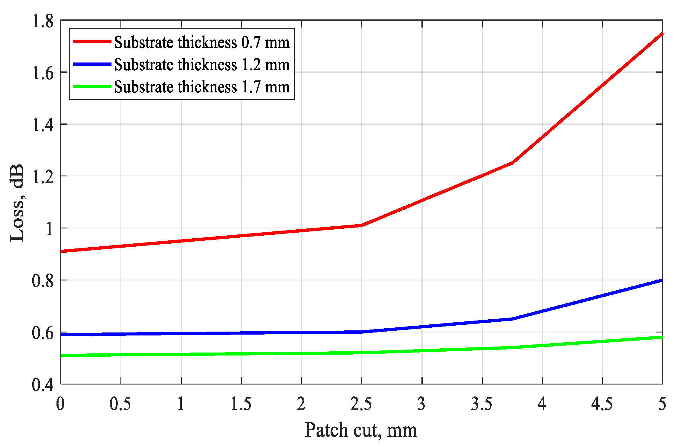
Choosing the antenna topology, as well as the substrate parameters, allows maintaining the low ripple level of the unit-cell response with extended bandwidth, and, as a result, to reduce the insertion loss. The proposed unit-cell antennas have reduced size with respect to the standard patch due to the additional cutout in the center of the patches, thus providing square ring design. To study the influence the antenna layout, as well as the substrate parameters on insertion loss the full-wave EM simulation of the proposed unit-cell design is provided, Figure 2. The insertion loss is presented as a function of the cutout lateral dimensions for different substrate thickness while maintaining the reflection coefficient modules lower than −20 dB. The lateral dimensions of the cutout area were chosen 5 × 5 mm2. As a result, the square ring antenna area was decreased up to 28% with respect to standard patch antenna, which is equal to 11.5 × 11.5 mm2 (0.44λg × 0.44λg) and 13 × 13 mm2 (0.5λg × 0.5λg), correspondingly. On the other hand, the reduced antenna area brings additional losses that estimated as 0.2 dB higher than for traditional design. Nevertheless, we expect reduced mutual coupling between unit-cells arranged to a transmitarray. In addition, a denser allocation of unit-cells in a transmitarray will allow us to reduce a gain loss for beam steering [19].
3. Switching States Approach
The proposed unit cell provides either two opposite phase-shift states, marked as 0° and 180°, depending on the connection of the U-shaped resonators placed at receiving and transmitting sides of the unit cell. The 180° phase shift is obtained by switching the feed point of the U-shaped resonator on one side of the transmitarray by using two p-i-n diodes, while at opposite sides of the unit cell U-shaped resonator is connected to the via hole by transmission line section (Figure 3a). The state is referred to as the 0° state when the resonators on both sides are connected in the same way so that the currents flowing in the antennas are codirectional. In the 180° state, the resonators are connected by opposite ends in such a way that currents flow in opposite directions. The two p-i-n diodes are connected in codirectional ways as shown in Figure 3b to provide p-i-n diodes opposite states operation. The forward biasing provides ON state for V2 and OFF state for V1 and vice versa. Depending on the sign of the bias voltage, the radiating current is in-phase or out-of-phase, which leads to a 1-bit differential phase shift.
Two AlGaAs flip-chip p-i-n diodes Macom MA4AGP907 are integrated into the unit-cell. A single very thin bias line is used to apply biasing voltage to the p-i-n diodes and does not interact with the antenna elements. To provide a decoupling DC and microwave currents the inductors (12 nH) are used. The DC control voltage is applied through inductances L1, L3 (two identical inductances are used for scheme symmetry), while L2 is grounded. Typically, an additional bypass shunt capacitance in the biasing network improves isolation. Moreover, the additional bypass capacitance allows avoiding a mutual coupling between neighbour unit-cells arranged to an array. To minimize the number of surface-mounted device (SMD) components, the bypass capacitor is implemented as a parallel plate capacitor between two metalized planes in the middle of the structure by introducing a gap in one ground plane while keeping another one without a gap. The bypass capacitance value with considering parallel plate capacitance (Cp) and gap capacitance (Cg) is estimated as 60 pF. Such an approach simplifies the unit cell DC biasing circuitry. Additionally, a biasing line is connected to the distributed parallel plate capacitor away from resonant structures, which avoids the interaction of the biasing line with the patch antenna elements.
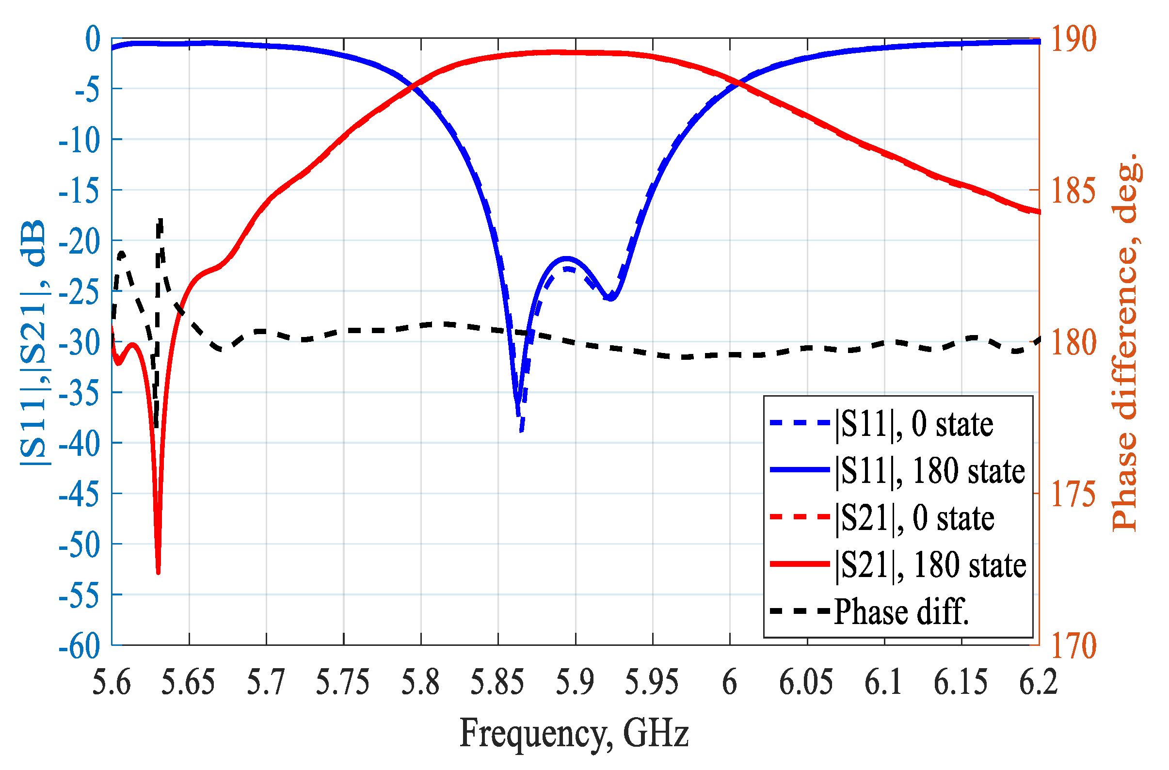
Certainly, the p-i-n diodes bring additional loss to the transmission coefficient of the unit cell by reducing the unloaded Q-factor of the resonator (which is a patch antenna). Typically, an increased loss is associated with ohmic loss in an open state, the off-state isolation, and parasitic parameters in both states. Thus, p-i-n diodes were modelled with a serial resistance 3.6 Ohm for on-state, off-state capacitance 27 pF and serial parasitic inductance 0.31 nH for both states. The mismatching due to the contribution of parasitic parameters of the p-i-n diodes leads to higher overall insertion loss equal to 1.6 dB. To improve the passband loss and decrease mismatching caused by p-i-n diode parasitic parameters the size of patch antenna at one side of the structure has been changed. The results of the simulation of the unit cell scattering parameters modules are represented in Figure 4. The insertion loss is equal to 1.3 dB at 5.9 GHz in both states while the reflection coefficient does not exceed −20 dB within the passband. The 3-dB transmission bandwidth is equal to 200 MHz (3.4%). The phase error does not exceed ± 1° in the passband.
The radiation characteristics of the proposed unit-cell are the point of interest. The unit-cell realized gain for different frequencies is shown in Figure 5. The gain is 5.5 dB at the central frequency, while the gain loss due to mismatching is about 2.5 dB in 200 MHz (3.4%) frequency bandwidth. It should be noted that the structure can be modified by placing an additional coupling element to the vertical arm of the square ring antennas to provide dual-polarization operation [12].
The unit cell has been fabricated using a standard PCB process and characterized inside the waveguide. The measurement setup includes two coax SMA to rectangular waveguide transitions with cross-section dimensions of 40 × 20 mm2 (5.6 ÷ 6.2 GHz). The measured frequency response obtained employing VNA R&S ZNB20 is presented in Figure 6. The forward bias current is equal to 15 mA. The measured S-parameters are identical for both states; the insertion loss is equal to 2.3 dB at 5.9 GHz in both states. The 3-dB transmission bandwidth is 180 MHz (3.4%). The phase error does not exceed ± 1° in the passband. A good agreement of the measured results with the simulated ones is obtained. The higher insertion loss is associated with higher metallic and dielectric losses and more narrowband response. Due to the soldering process of the diodes a change in the coupling between the antennas occurs, the reflection coefficient resonances are stuck together.
The comparative study of unit cell realizations with p-i-n-diodes is summarized in Table 1. The study shows that the proposed unit-cell has insertion loss and dimensions commensurable with other structures yet excellent phase error of ±1° within the given bandwidth. Using p-i-n-diodes inside the radiating element ensures the distortion of the radiation parameters of the unit-cell [9,13,14]. The other unit cells not inserting p-i-n-diodes into radiating elements have to combine two separate PCBs [11,15]. Whereas the structure presented in this paper can be implemented within a single PCB process and then populated with p-i-n-diodes, which makes this approach more robust and advantageous for mass-manufacturing.
4. Conclusions
The reconfigurable unit cell with two-phase states suitable for C-band transmitarray applications is presented. The structure of the unit cell consists of two square ring patches of reduced size, which are connected by the coupling element. The switching states of the p-i-n diodes allow changing the direction of current flow in the antennas providing 180° phase difference with negligible phase error. The proposed square ring patch antenna unit-cell has reduced lateral dimensions equal to 0.44λg × 0.44λg with respect to the standard 0.5λg × 0.5λg patch. The paper provides a detailed analysis of the unit-cell insertion loss contribution, which allows optimizing the structure design from the point of view of insertion loss, the bandwidth, and the antennas area. Additionally, the p-i-n diodes bring the loss associated with ohmic resistance and parasitic parameters. The possibility of compensating the loss caused by the p-i-n diodes due to mismatching is demonstrated. As a result of EM simulation, the scattering characteristics reveal a passband insertion loss of less than 1.6 dB, while ensuring the flat 180° phase difference with phase error ±1°. The simulation results have been validated by measurements. The measured transmission coefficient module reveals higher insertion loss (2.3 dB), which is associated with higher metallic and dielectric losses and more narrowband response. Nevertheless, the flat 180° phase difference with 1° phase error and perfect matching makes this structure an attractive candidate for reconfigurable transmitarray with beam-steering capability for sub-6 GHz 5G communication systems application.
Author Contributions
Software, validation, investigation, data analysis, visualization, V.K.; original draft preparation, writing—review and editing, I.M. and P.T.; conceptualization and supervision, P.T.; All authors have read and agreed to the published version of the manuscript.
Funding
This work has been supported by the Russian Science Foundation (project 17-79-20374).
Acknowledgments
The authors would like to thank D. Kozlov for fruitful discussions of the work.
Conflicts of Interest
The authors declare no conflict of interest.
References
- Di Renzo, M.; Debbah, M.; Phan-Huy, D.T.; Zappone, A.; Alouini, M.S.; Yuen, C.; Sciancalepore, V.; Alexandropoulos, G.C.; Hoydis, J.; Gacanin, H.; et al. Smart radio environments empowered by reconfigurable AI meta-surfaces: An idea whose time has come. EURASIP J. Wirel. Commun. Netw. 2019, 2019, 1–20. [Google Scholar] [CrossRef] [Green Version]
- Kozlov, D.S.; Odit, M.A.; Vendik, I.B.; Roh, Y.G.; Cheon, S.; Lee, C.W. Tunable terahertz metamaterial based on resonant dielectric inclusions with disturbed Mie resonance. Appl. Phys. A 2012, 106, 465–470. [Google Scholar] [CrossRef]
- Zhou, Z.; Ge, N.; Wang, Z.; Chen, S. Hardware-efficient hybrid precoding for millimeter wave systems with multi-feed reflectarrays. IEEE Access 2018, 6, 6795–6806. [Google Scholar] [CrossRef]
- Abdelrahman, A.H.; Elsherbeni, A.; Nayeri, P.; Yalng, F. Analysis and design of transmitarray antennas. Synth. Lect. Antennas 2017, 6, 1–175. [Google Scholar] [CrossRef]
- Sazegar, M.; Zheng, Y.; Kohler, C.; Maune, H.; Nikfalazar, M.; Binder, J.R.; Jakoby, R. Beam steering transmitarray using tunable frequency selective surface with integrated ferroelectric varactors. IEEE Trans. Antennas Propag. 2012, 60, 5690–5699. [Google Scholar] [CrossRef]
- Minatti, G.; Martini, E.; Caminita, F.; Pavone, S.C.; Albani, M.; Toso, G.; Maci, S. Electronically Reconfigurable Metasurface Antennas based on Liquid Crystal Technology. In Proceedings of the 13th European Conference on Antennas and Propagation (EuCAP), Kraków, Poland, 31 March–5 April 2019; pp. 1–3. [Google Scholar]
- Reis, J.R.; Caldeirinha, R.F.; Hammoudeh, A.; Copner, N. Electronically reconfigurable FSS-inspired transmitarray for 2-D beamsteering. IEEE Trans. Antennas Propag. 2017, 65, 4880–4885. [Google Scholar] [CrossRef]
- Mailloux, R. Array grating lobes due to periodic phase, amplitude, and time delay quantization. IEEE Trans. Antennas Propag. 1984, 32, 1364–1368. [Google Scholar] [CrossRef] [Green Version]
- Clemente, A.; Dussopt, L.; Sauleau, R.; Potier, P.; Pouliguen, P. 1-Bit Reconfigurable Unit Cell Based on PIN Diodes for Transmit-Array Applications in X-Band. IEEE Trans. Antennas Propag. 2012, 60, 2260–2269. [Google Scholar] [CrossRef]
- Di Palma, L.; Clemente, A.; Dussopt, L.; Sauleau, R.; Potier, P.; Pouliguen, P. Circularly-polarized reconfigurable transmitarray in Ka-band with beam scanning and polarization switching capabilities. IEEE Trans. Antennas Propag. 2016, 65, 529–540. [Google Scholar] [CrossRef]
- Nguyen, B.D.; Pichot, C.; Nguyen, D.B. Unit-cell loaded with PIN diodes for 1-bit linearly polarized reconfigurable transmitarrays. IEEE Antennas Wirel. Propag. Lett. 2018, 18, 98–102. [Google Scholar] [CrossRef]
- Munina, I.; Turalchuk, P.; Verevkin, A.; Kirillov, V.; Zelenchuk, D.; Shitvov, A. A Tiled C-Band Dual-Polarized 1-Bit Transmitarray. In Proceedings of the 49th European Microwave Conference (EuMC), Paris, France, 2–4 October 2019; pp. 1092–1095. [Google Scholar]
- Pan, W.; Huang, C.; Ma, X.; Jiang, B.; Luo, X. A dual linearly polarized transmitarray element with 1-bit phase resolution in X-band. IEEE Antennas Wirel. Propag. Lett. 2014, 14, 167–170. [Google Scholar] [CrossRef]
- Wang, Y.; Xu, S.; Yang, F.; Li, M. A Novel 1-bit Wide-angle Beam Scanning Reconfigurable Transmitarray Antenna Using an Equivalent Magnetic Dipole Element. IEEE Trans. Antennas Propag. 2020. [Google Scholar] [CrossRef]
- Wang, M.; Xu, S.; Yang, F.; Li, M. Design and Measurement of a 1-bit Reconfigurable Transmitarray with Subwavelength H-Shaped Coupling Slot Elements. IEEE Trans. Antennas Propag. 2019, 67, 3500–3504. [Google Scholar] [CrossRef]
- Simine, A.; Kholodnyak, D.; Turalchuk, P.; Piatnitsa, V.; Jantunen, H.; Vendik, I. Enhancement of inductance Q-factor for LTCC filter design. In Proceedings of the European Microwave Conference, Paris, France, 2 October 2005; p. 4. [Google Scholar]
- Piatnitsa, V.; Kholodnyak, D.; Tick, T.; Simin, A.; Turalchuk, P.; Zameshaeva, E.; Vendik, I. Design and investigation of miniaturized high-performance LTCC filters for wireless communications. In Proceedings of the European Microwave Conference, Munich, Germany, 9 October 2007; pp. 544–547. [Google Scholar]
- Khanna, A.P.S.; Garault, Y. Determination of loaded, unloaded, and external quality factors of a dielectric resonator coupled to a microstrip line. IEEE Trans. Microw. Theory Tech. 1983, 31, 261–264. [Google Scholar] [CrossRef]
- Mailloux, R.J. Phased Array Antenna Handbook; Artech House Inc.: New York, NY, USA, 1994. [Google Scholar]
Figure 1.
Non-reconfigurable unit cell structure (a), and EM simulation results of the unit cells scattering parameters modules for different coupling between patch antennas (b).
Figure 1.
Non-reconfigurable unit cell structure (a), and EM simulation results of the unit cells scattering parameters modules for different coupling between patch antennas (b).

Figure 2.
The dependence of the unit-cell insertion loss on cutout lateral size for different substrate thickness.
Figure 2.
The dependence of the unit-cell insertion loss on cutout lateral size for different substrate thickness.

Figure 3.
The proposed reconfigurable 1-bit unit cell structure (a), DC biasing network design of the unit-cell (b).
Figure 3.
The proposed reconfigurable 1-bit unit cell structure (a), DC biasing network design of the unit-cell (b).

Figure 4.
The simulated results of the unit cells scattering parameters modules for both p-i-n diodes states and phase difference.
Figure 4.
The simulated results of the unit cells scattering parameters modules for both p-i-n diodes states and phase difference.

Figure 5.
The unit-cell radiation pattern for 5.8 GHz, 5.9 GHz, and 6 GHz.

Figure 6.
Measured scattering parameters and differential phase shift of the proposed reconfigurable unit cell structure and insets fabricated prototype of the reconfigurable unit cell structure inside a rectangular waveguide.
Figure 6.
Measured scattering parameters and differential phase shift of the proposed reconfigurable unit cell structure and insets fabricated prototype of the reconfigurable unit cell structure inside a rectangular waveguide.


Table 1.
Comparison of reconfigurable unit cell realization using p-i-n-diodes.
| Ref. | Type | Size | f0 (Δf/f0) | Loss | Phase Error | Placement of p-i-n Diodes |
|---|---|---|---|---|---|---|
| [9] | O-slot rectangular patch | 0.5λ × 0.5λ | 10 GHz (~15%) | 1.9 dB | <13° | radiating element |
| [11] | circular patch with slot | 0.54λ × 0.54λ | 11.5 GHz, n/a | 1.4 dB | n/a | coupling elements |
| [13] | square ring patch | 0.5λ × 0.5λ | 10 GHz, ~4% | 1.75 dB | ±6° | radiating element |
| [14] | magnetic dipole | 0.5λ × 0.5λ | 13.5 GHz (~13%) | 2 dB | n/a | radiating element |
| [15] | H-shaped slots | λ/3 × λ/3 | 12.5 GHz (~10%) | 3 dB | n/a | phase delay line |
| [This work] | square ring patch | 0.46λ × 0.46λ | 5.9 GHz (3.4%) | 2.3 dB | ±1° | coupling elements |
© 2020 by the authors. Licensee MDPI, Basel, Switzerland. This article is an open access article distributed under the terms and conditions of the Creative Commons Attribution (CC BY) license (http://creativecommons.org/licenses/by/4.0/).
Share and Cite
MDPI and ACS Style
Kirillov, V.; Munina, I.; Turalchuk, P. Small-Size Square Ring 1-Bit Reconfigurable Transmitarray Unit Cell for C-Band Applications. Appl. Sci. 2020, 10, 3319. https://doi.org/10.3390/app10093319
AMA Style
Kirillov V, Munina I, Turalchuk P. Small-Size Square Ring 1-Bit Reconfigurable Transmitarray Unit Cell for C-Band Applications. Applied Sciences. 2020; 10(9):3319. https://doi.org/10.3390/app10093319
Chicago/Turabian StyleKirillov, Vitalii, Irina Munina, and Pavel Turalchuk. 2020. "Small-Size Square Ring 1-Bit Reconfigurable Transmitarray Unit Cell for C-Band Applications" Applied Sciences 10, no. 9: 3319. https://doi.org/10.3390/app10093319
Note that from the first issue of 2016, this journal uses article numbers instead of page numbers. See further details here.