
A Linear Microwave Plasma Source Using a Circular Waveguide Filled with a Relatively High-Permittivity Dielectric: Comparison with a Conventional Quasi-Coaxial Line Waveguide

Abstract
:1. Introduction
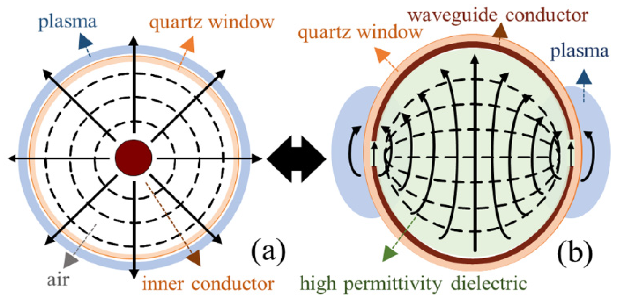
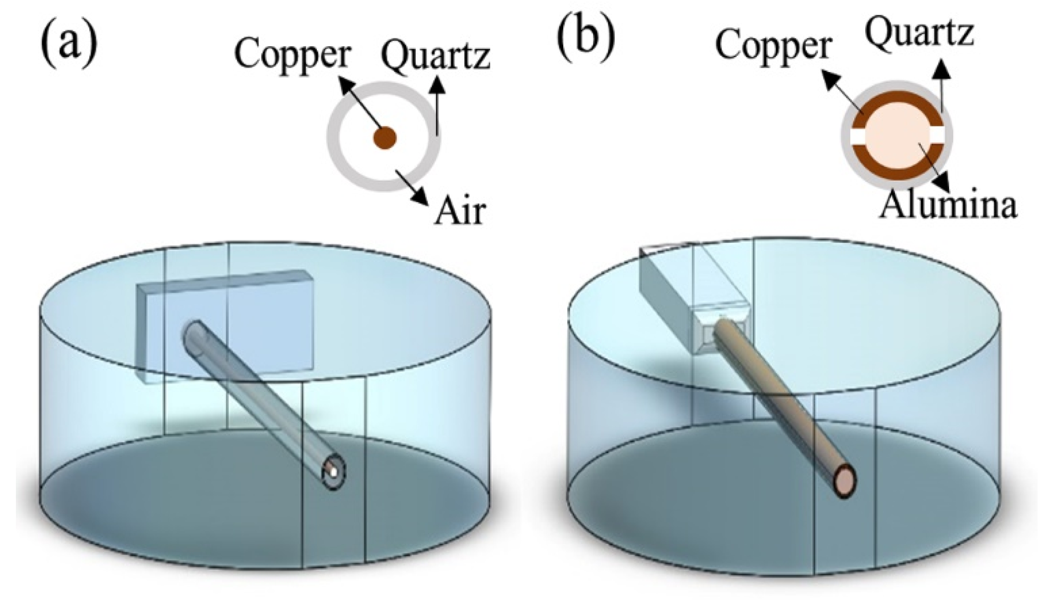
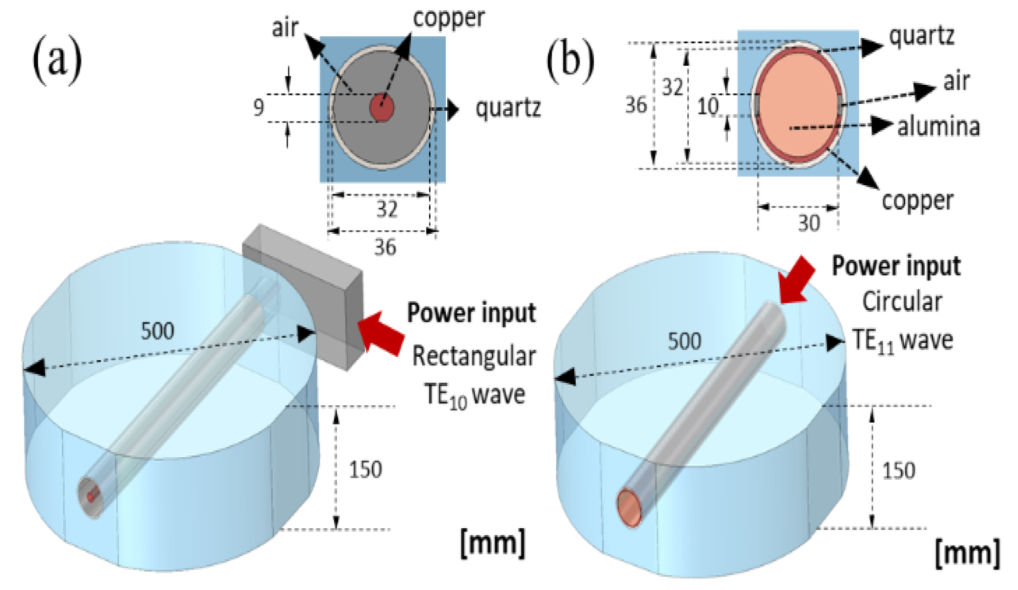
2. Plasma Source Overview
3. Experiment
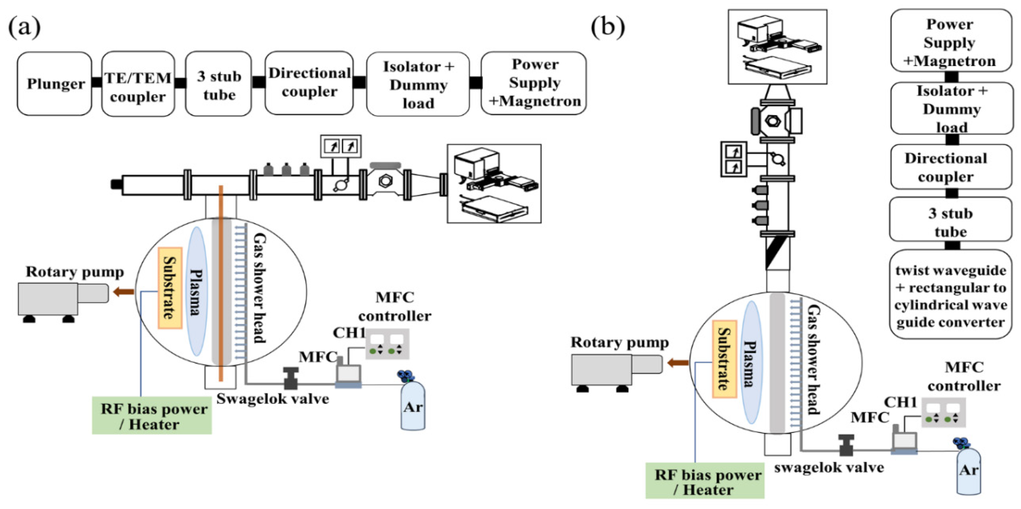
Experiment Setup
4. Simulation
4.1. Simulation Methods
4.2. The Computational Mesh & Geometry
4.3. Governing Equations
4.3.1. The Electromagnetic Field Model
4.3.2. Plasma Model
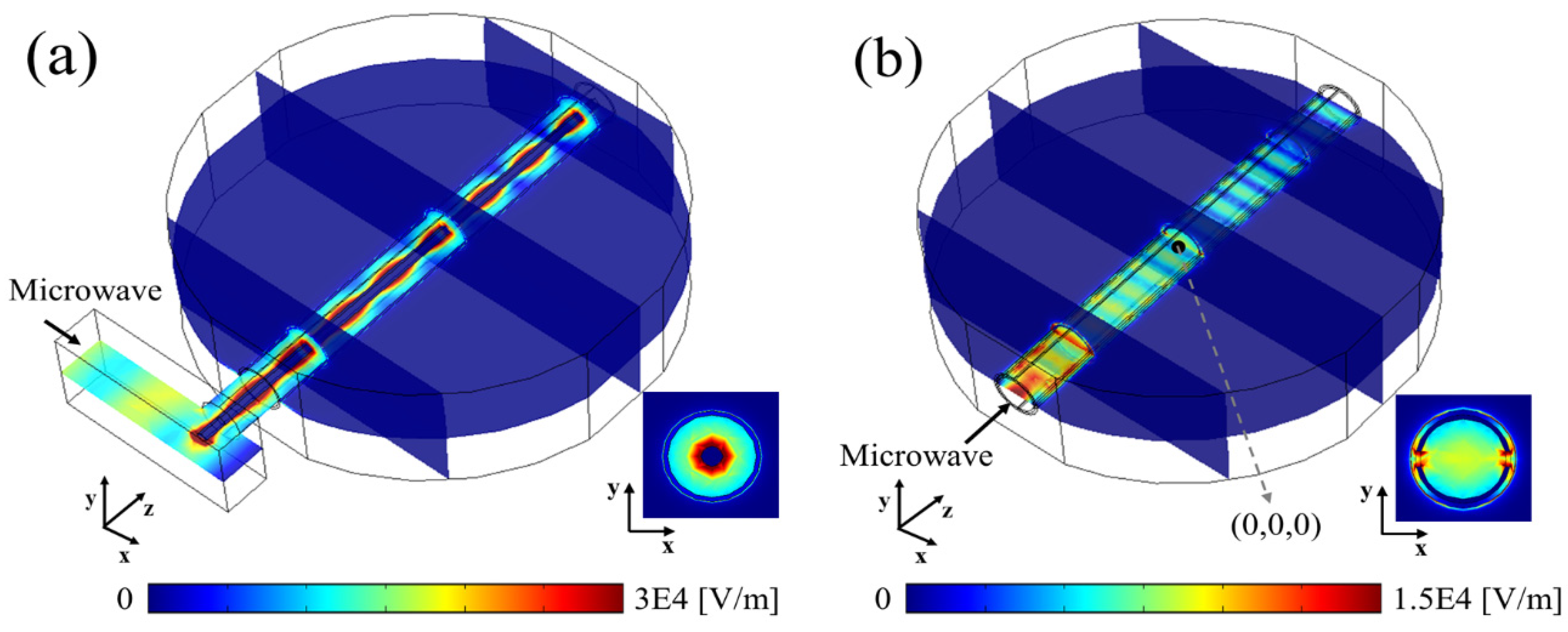
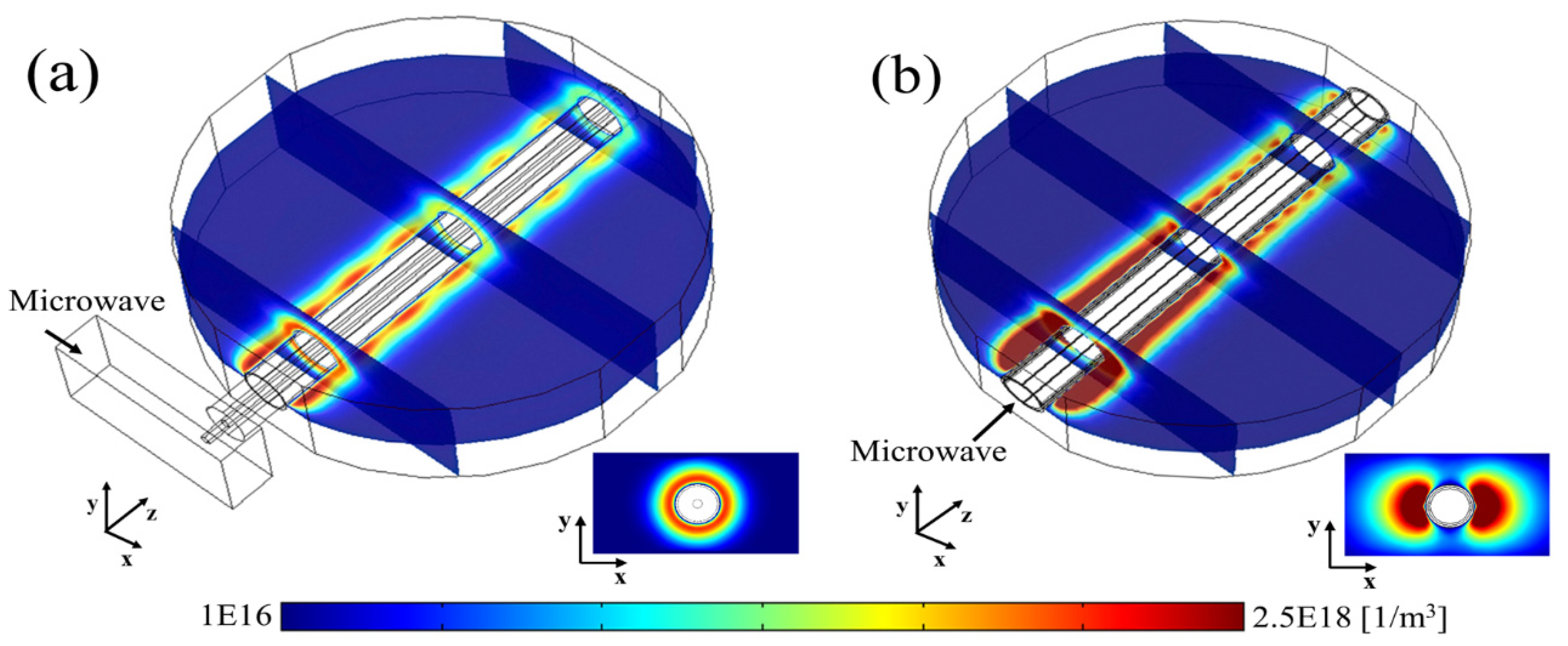
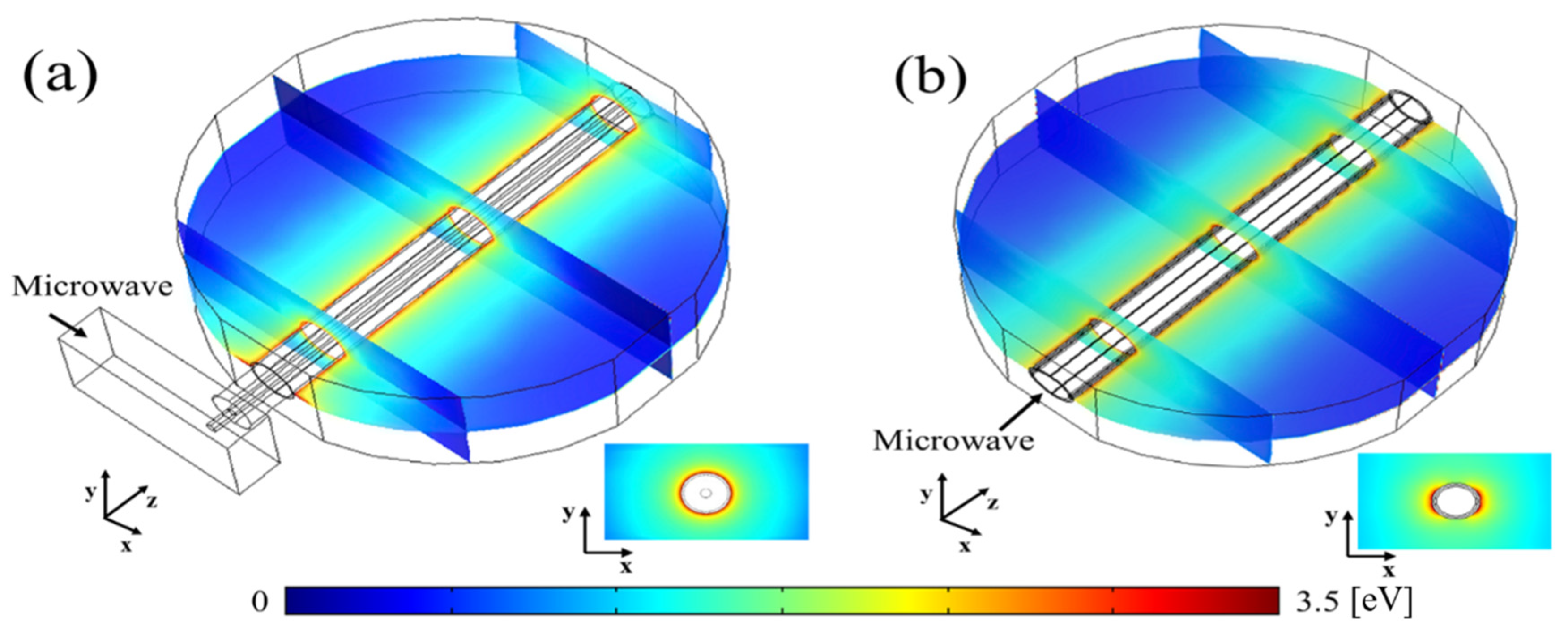
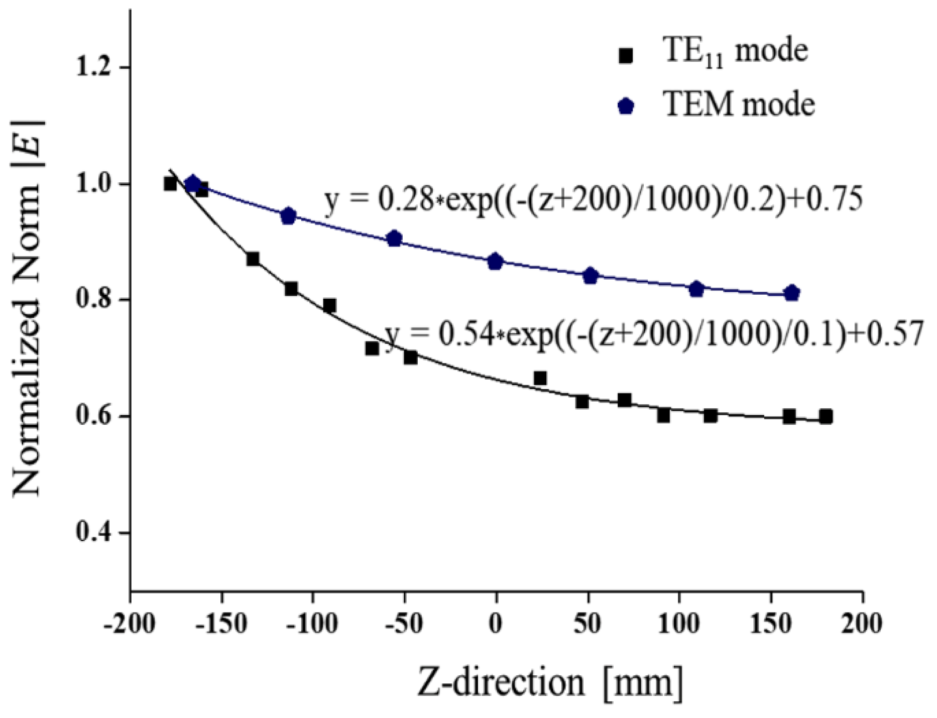
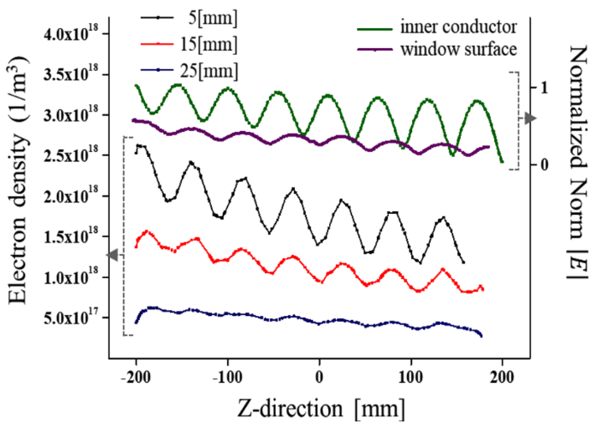
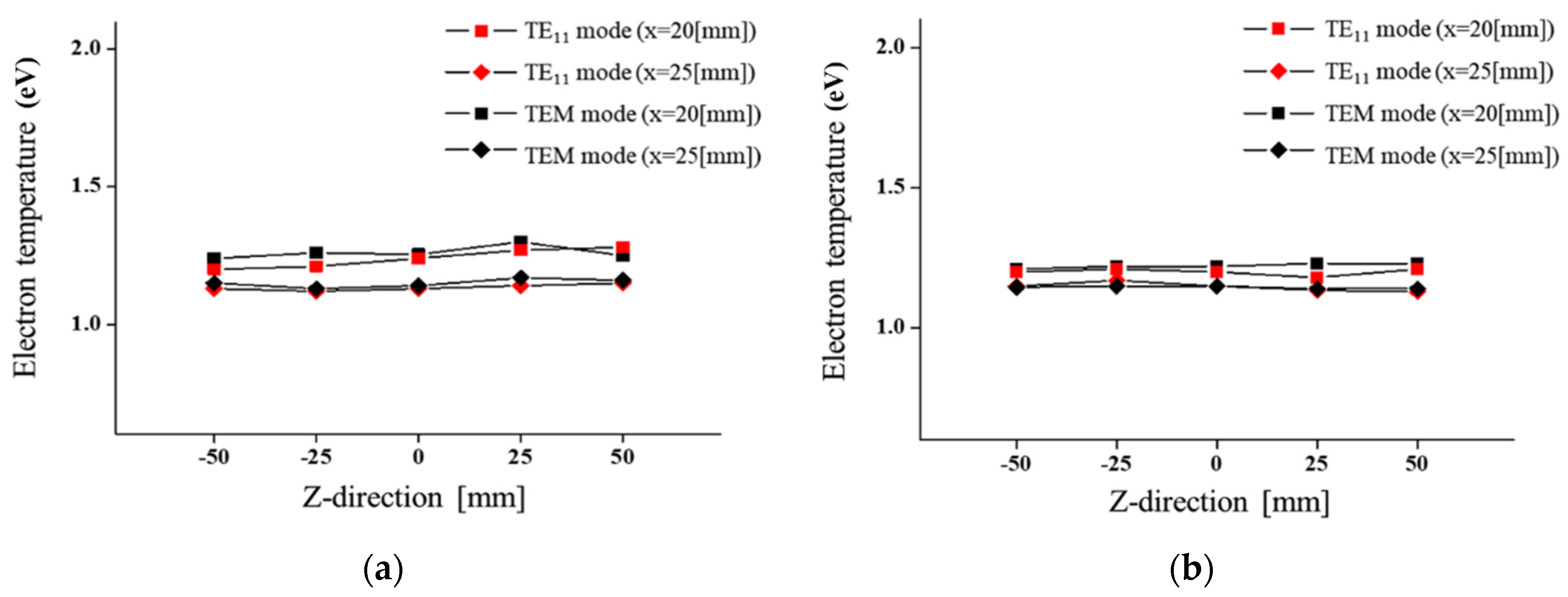
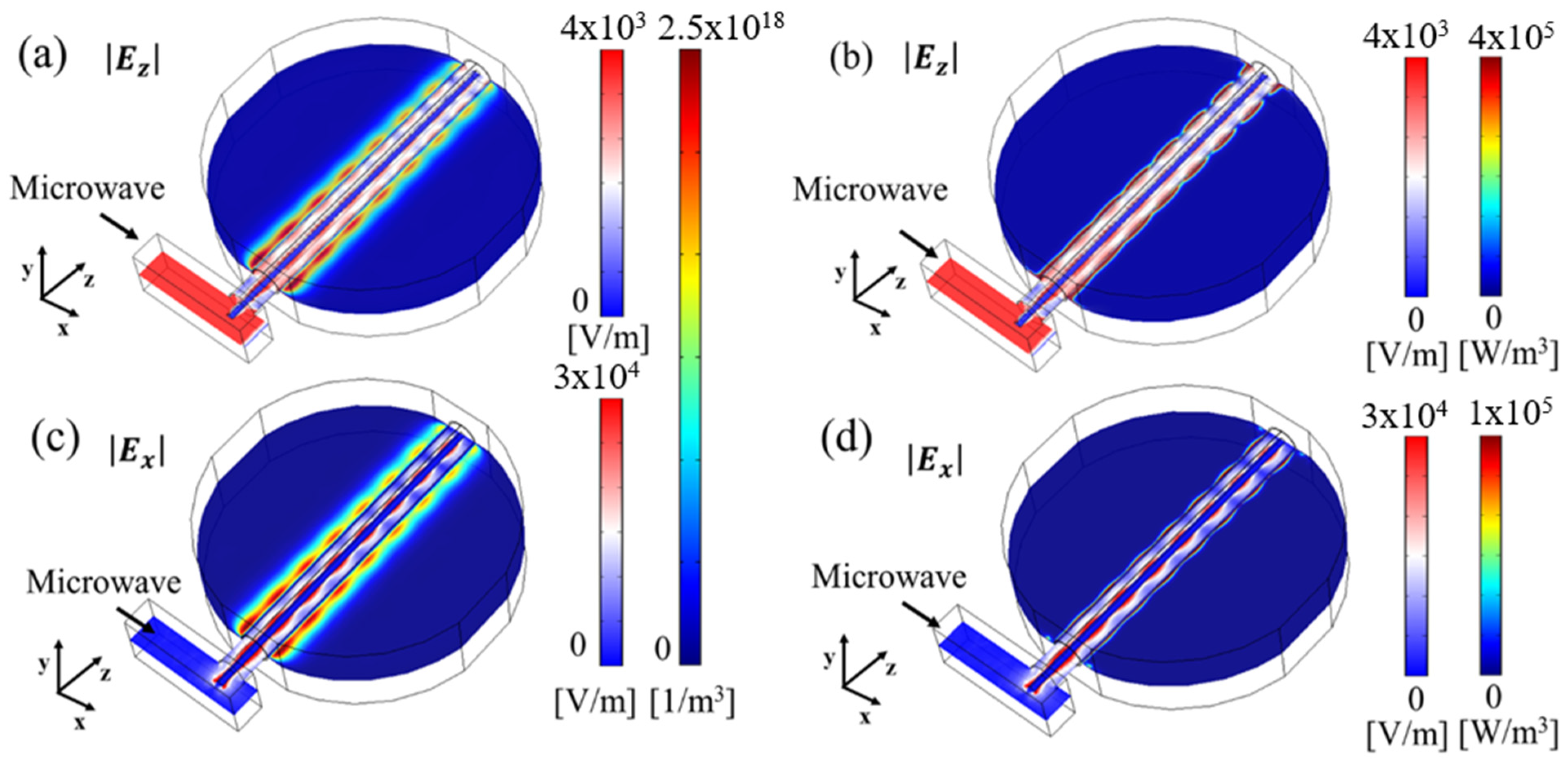
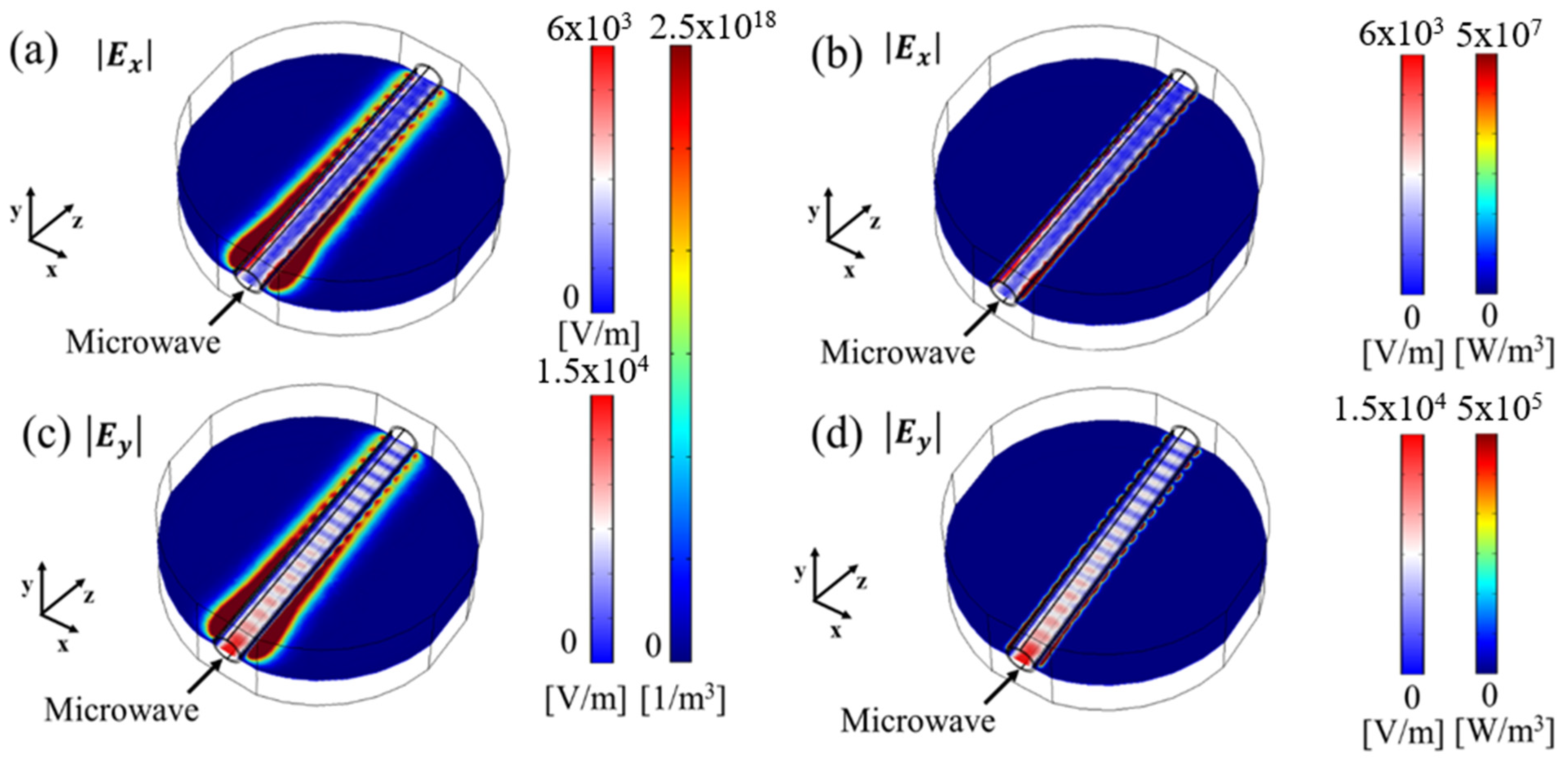
5. Results and Discussion
6. Conclusions
Author Contributions
Funding
Institutional Review Board Statement
Informed Consent Statement
Data Availability Statement
Acknowledgments
Conflicts of Interest
References
- Pozar, D.M. Microwave Engineering, 4th ed.; John Wiley & Sons: New Jersey, NJ, USA, 2011. [Google Scholar]
- Collin, R.E. Foundations for Microwave Engineering, 2nd ed.; McGraw Hill: New York, NY, USA, 1992. [Google Scholar]
- Ferreira, C.M.; Moisan, M. 1993 Microwave Discharges Fundamentals and Applications; Springer: New York, NY, USA, 1993. [Google Scholar]
- Lebedev, Y.A. Microwave discharges at low pressures and peculiarities of the processes in strongly non-uniform plasma. Plasma Sources Sci. Technol. 2015, 24, 053001. [Google Scholar] [CrossRef]
- Zakrzewski, Z.; Moisan, M. Plasma Sources using long linear microwave field applicators: Main features, classification and modeling. Plasma Sources Sci. Technol. 1995, 4, 379–397. [Google Scholar] [CrossRef]
- Kromka, A.; Babchenko, O.; Izak, T.; Hruska, K.; Rezek, B. Linear antenna microwave plasma CVD deposition of diamond films over large areas. Vacuum 2012, 86, 776–779. [Google Scholar] [CrossRef]
- Moisan, M.; Zakrzewski, Z. Plasma sources based on the propagation of electromagnetic surface waves. J. Phys. D Appl. Phys. 1991, 24, 1025. [Google Scholar] [CrossRef] [Green Version]
- Kiyokawa, K.; Sugiyama, K.; Tomimatsu, M.; Kurokawa, H.; Miura, H. Microwave-included non-equilibrium plasma by insertino of substrate at low and atmospheric pressures. Appl. Surf. Sci. 2001, 169, 599. [Google Scholar] [CrossRef]
- Jauberteau, I.; Jauberteau, J.L.; Goudeau, P.; Soulestin, B.; Marteau, M.; Cahoreau, M.; Aubreton, J. Investigation on a nitriding process of molybdenum thin films exposed to (Ar-N2-H2) expanding microwave plasma. Surf. Coat. Technol. 2009, 203, 1127. [Google Scholar] [CrossRef]
- Rauchle, E. Duo-plasmaline, a surface wave sustained linearly extended discharge. J. Phys. IV 1998, 8, Pr7-99–Pr7-108. [Google Scholar] [CrossRef]
- Petasch, W.; Rauchle, E.; Muegge, H.; Muegge, K. Duo-Plasmaline a linearly extended homogeneous low pressure plasma source. Surf. Coat. Technol. 1997, 93, 112. [Google Scholar] [CrossRef]
- Liehr, M.; Wieder, S.; Dieguez-Campo, M. Large area microwave coating technology. Thin Solid Films 2006, 502, 9. [Google Scholar] [CrossRef]
- Liehr, M.; Dieguez-Campo, M. Microwave PECVD for large area coating. Surf. Coat. Technol. 2005, 200, 21–25. [Google Scholar] [CrossRef]
- Han, M.K.; Cha, J.H.; Lee, H.J.; Chang, C.J.; Jeon, C.Y. The Effects of CF4 Partial Pressure on the Hydrophobic Thin Film Formation on Carbon Steel by Surface Treatment and Coating Method with Linear Microwave Ar/CH4/CF4 Plasma. J. Electr. Eng. Technol. 2017, 12, 2007–2013. [Google Scholar]
- Neykova, N.; Kozak, H.; Ledinsky, M.; Kromka, A. Novel plasma treatment in linear antenna microwave PECVD system. Vacuum 2012, 86, 603–607. [Google Scholar] [CrossRef]
- Sahu, B.B.; Joga, S.; Toyoda, H.; Han, J.G. Development and plasma characterization of an 850 MHz surface-wave plasma source. AIP Adv. 2017, 7, 105213. [Google Scholar] [CrossRef]
- Yamada, T.; Kim, J.H.; Ishihara, M.; Hasegawa, M. Low-temperature graphene synthesis using microwave plasma CVD. J. Phys. D Appl. Phys. 2013, 46, 063001. [Google Scholar] [CrossRef]
- Tarey, R.D.; Jarwal, R.K.; Ganguli, A.; Akhtar, M.K. High-density plasma production using a slotted helical antenna at high microwave power. Plasma Sources Sci. Technol. 1997, 6, 189. [Google Scholar] [CrossRef]
- Suetsugu, Y.; Kawai, Y. Temporal Behaviour of ECR Plasmas Produced by a Lisitano Coil. Jpn. J. Appl. Phys. 1984, 23, 237. [Google Scholar] [CrossRef]
- Kaswai, Y.; Sakamoto, K. Production of a large diameter hot-electron plasma by electron cyclotron resonance heating. Rev. Sci. Instrum. 1982, 53, 606. [Google Scholar] [CrossRef]
- Latrasse, L.; Radoiu, M.; Lo, J.; Guillot, P. 2.45-GHz microwave plasma sources using solid-state microwave generators. ECR-type plasma source. J. Microw. Power Electromagn. Energy 2016, 50, 308–321. [Google Scholar] [CrossRef]
- Ruzic, D.N. Electric Probes for Low Temperature Plasmas; American Vacuum Society: New York, NY, USA, 1994. [Google Scholar]
- Godyak, V.A.; Piejak, R.B.; Alexandrovich, B.M. Measurements of electron energy distribution in low-pressure RF discharges. Plasma Sources Sci. Technol. 1992, 1, 36. [Google Scholar] [CrossRef]
- Kim, J.Y.; Choe, W.H.; Dang, J.J.; Chung, K.J.; Hwang, Y.S. Characterization of electron kinetics regime with electron energy probability functions in inductively coupled hydrogen plasmas. Phys. Plasmas 2016, 23, 023511. [Google Scholar] [CrossRef]
- Ghanashev, I.; Nagatsu, M.; Xu, G.; Sugai, H. Mode Jumps and Hysteresis in Surface-Wave Sustained Microwave Discharges. Jpn. J. Appl. Phys. 1997, 36, 4704–4710. [Google Scholar] [CrossRef]
- Ferreira, C.M. A basic self-contained model of a plasma column sustained by a weakly damped surface wave. J. Phys. D Appl. Phys. 1988, 22, 705–708. [Google Scholar] [CrossRef]
- Granier, A.; Boisse-Laporte, C.; Leprince, P.; Marec, J.; Nghiem, P. Wave propagation and diagnostics in argon surface-wave discharges up to 100 Torr. J. Phys. D Appl. Phys. 1986, 20, 204–209. [Google Scholar] [CrossRef]
- Sugai, H. Observation of Collisionless electron-cycltron damping in a plasma. Phys. Rev. A 1981, 24, 1571. [Google Scholar] [CrossRef]
- Kousaka, H.; Ono, K. Fine structure of the electromagnetic fields formed by backward surface waves in an azimuthally symmetric surface wave-excited plasma source. Plasma Sour. Sci. Technol. 2003, 12, 273. [Google Scholar] [CrossRef]
- Gordiets, B.; Pinheiro, M.; Tatarova, E.; Dias, F.M.; Ferreira, C.M.; Ricard, A. A traveling wave sustained hydrogen discharge: Modeling and experiment. Plasma Sour. Sci. Technol. 2000, 9, 295. [Google Scholar] [CrossRef]
- Paunska, T.; Schluter, H.; Shivarova, A.; Tarnev, K. Surface-wave produced discharges in hydrogen: II. Modifications of the discharge structure for varying gas-discharge conditions. Plasma Sour. Sci. Technol. 2003, 12, 608. [Google Scholar] [CrossRef]
- Ferreira, C.M.; Tatarova, E.; Guerra, V.; Gordiets, B.F.; Henriques, J.; Dias, F.M.; Pinheiro, M. Modeling of Wave Driven Molecular(H2, N2, N2-Ar) Discharges as Atomic Sources. IEEE Trans. Plasma. Sci. 2003, 31, 4. [Google Scholar] [CrossRef]
- Rahimi, S.; Jimenez-Diaz, M.; Hubner, S.; Kemaneci, E.H.; Vander Mullen, J.J.A.M.; Dijk, J.V. A two-dimensional modelling study of a coaxial plasma waveguide. J. Phys. D Appl. Phys. 2014, 47, 125204. [Google Scholar] [CrossRef]
- Obrusnik, A.; Bonaventura, Z. Studying a low-pressure microwave coaxial discharge in hydrogen using a mixed 2D/3D fluid model. J. Phys. D Appl. Phys. 2015, 48, 065201. [Google Scholar] [CrossRef]
- COMSOL Plasma Module User’s Guide (COMSOL Multiphysics); COMSOL: Massachusetts, MA, USA, 2019.
- Ganguli, A.; Akhtar, M.K.; Tarey, R.D.; Jarwal, R.K. Absorption of left-polarized microwaves in electron cyclotron resonance plasmas. Phys. Lett. A 1998, 250, 137. [Google Scholar] [CrossRef]
- Lymberopoulos, D.P.; Economou, D.J. Fluid simulation of glow discharges:Effect of metastable atoms in argon. J. Appl. Phys. 1993, 73, 3668. [Google Scholar] [CrossRef] [Green Version]
- Yamabe, C.; Buckman, S.J.; Phelps, A.V. Measurement of free-free emission from low-energy-electron collisions with Ar. Phys. Rev. A 2008, 27, 1345. [Google Scholar] [CrossRef]
- Ali, M.A.; Stone, P.M. Electron impact ionization of metastable rare gases: He, Ne and Ar. Int. J. Mass Spectrom. 2008, 271, 51. [Google Scholar] [CrossRef]
- Cramer, W.H. Elastic and Inelastic scattering of Low-Velocity Ions: Ne+ in A, A+ in Ne and A+ in A. J. Chem. Phys. 1959, 30, 641. [Google Scholar] [CrossRef]
- Kim, J.S.; Hur, M.Y.; Kim, H.J.; Lee, H.J. Advanced PIC-MCC simulation for the investigation of step-ionization effect in intermediate-pressure capacitively coupled plasmas. J. Phys. D Appl. Phys. 2018, 51, 104004. [Google Scholar] [CrossRef]
- Ostmark, H.; Roman, N. Laser ignition of pyrotechnic mixtures: Igniation mechanisms. J. Appl. Phys. 1993, 73, 1993. [Google Scholar] [CrossRef]
- Mcvey, B.; Scharer, J. Measurement of Collisionless Electron-Cyclotron Damping along a Weak Magnetic Beach. Phys. Rev. Lett. 1973, 31, 14. [Google Scholar] [CrossRef]
- Kawai, Y.; Uchino, K.; Muta, H.; Kawai, S.; Rowf, T. Development of large diameter ECR plasma source. Vacuum 2010, 84, 1381. [Google Scholar] [CrossRef]
- Verma, A.; Singh, P.; Narayanan, R.; Sahu, D.; Kar, S.; Ganguli, A.; Tarey, R.D. Investigations on argon and hydrogen plasmas produced by compact ECR plasma source. Plasma Res. Express 2019, 1, 035012. [Google Scholar] [CrossRef]
- Musil, J. Development of a new microwave plasma torch and its application to diamond synthesis. Vacuum 1986, 36, 161. [Google Scholar] [CrossRef]
- Popov, O.A. Effects of magnetic field and microwave power on electron cyclotron resonance type plasma characteristics. J. Vac. Sci. Technol. 1991, 9, 711. [Google Scholar] [CrossRef]
- Ganguli, A.; Tarey, R.D.; Arora, N.; Narayanan, R. Development and Studies on a compact electron cyclotron resonance plasma source. Plasma Sour. Sci. Technol. 2016, 25, 025026. [Google Scholar] [CrossRef]
- Lucovsky, G.; Tsu, D.V. Plasma enhanced chemical vapor deposition:Differences between direct and remote plasma excitation. J. Vac. Sci. Technol. A 1987, 5, 2231. [Google Scholar] [CrossRef]
- Hagelaar, C.J.M.; Pitchford, L.C. Solving the Boltzmann equation to obtain electron transport coefficients and rate coefficients for fluid models. Plasma Sour. Sci. Technol. 2005, 14, 722–733. [Google Scholar] [CrossRef]
- Gogolides, E.; Sawin, H.H. Continuum modeling of radio-frequency glow discharges. I. Theory and results for electropositive and electronegative gases. J. Appl. Phys. 1992, 72, 3971. [Google Scholar] [CrossRef]
- Gogolides, E.; Sawin, H.H. Continuum modeling of radio-frequency glow discharges. II. Parametric stuides ans sensitivity analysis. J. Appl. Phys. 1992, 72, 3988. [Google Scholar] [CrossRef]
- Passchier, J.D.P.; Goedheer, W.J. A two-dimensinal fluid model for and argon rf discharge. J. Appl. Phys. 1993, 74, 3744. [Google Scholar] [CrossRef]
- Richards, A.D.; Thompson, B.E.; Sawin, H.H. Continuum modeling of argon radio frequency glow discharges. Appl. Phys. Lett. 1987, 50, 492. [Google Scholar] [CrossRef]
- Ferreira, C.M. Modelling of a low-pressure plasma column sustained by a surface wave. J. Phys. D Appl. Phys. 1983, 16, 1673. [Google Scholar] [CrossRef]
- Suzuki, H.; Nakano, S.; Itoh, H.; Sekine, M.; Hori, M.; Toyoda, H. Characteristics of an atmospheric-pressure line plasma excited by 2.45 GHz microwave travelling wave. Jpn. J. Appl. Phys. 2016, 55, 01AH09. [Google Scholar] [CrossRef]
- Ellis, H.W.; Mcdaniel, E.W.; Albritton, D.L.; Viehland, L.A.; Lin, S.L.; Mason, E.A. Transport properties of gaseous ions over a wide energy range. Part II. Atomic Datat Nucl. Data Tables 1978, 17, 177–210. [Google Scholar] [CrossRef]
- Bird, R.B.; Stewart, W.E.; Lightfoot, E.N. Transport Phenomena; John Wiley & Sons: Hoboken, NJ, USA, 2002. [Google Scholar]
- Brokaw, R.S. Predicting Transport Properties of Dilute Gases. Ind. Eng. Process Des. Dev. 1969, 8, 240–253. [Google Scholar] [CrossRef]
- Cha, J.H.; Seo, K.S.; Jeong, J.H.; Lee, H.J. Two-dimensional fluid simulation of pulsed-power inductively coupled Ar/H2 discharge. J. Phys. D Appl. Phys 2021, 54, 16205. [Google Scholar] [CrossRef]
- Ganguli, A.; Akhtar, K.; Tarey, R.D. Absorption of high-frequency guided waves in a plasma-loaded waveguide. Phys. Plasmas 2007, 14, 102107. [Google Scholar] [CrossRef]


| Reaction Formula | Type | ||
|---|---|---|---|
| e + Ar → e + Ar | Elastic scattering | - | [38] |
| e + Ar → e + Ar* | Excitation | 11.55 | [38] |
| e + Ar* → e + e + Ar+ | Step-ionization | 4.16 | [39] |
| e + Ar → e + e + Ar+ | Direct-ionization | 15.76 | [38] |
| Ar + Ar+ → Ar + Ar+ | Scattering | - | [40] |
| Ar + Ar+ → Ar + Ar+ | Charge exchange | - | [40] |
| e + Ar* → e + Ar | Quenching | - | [41] |
| Ar + Ar* → Ar + Ar | Quenching | - | [41] |
| Ar* + Ar* → e + Ar+ + Ar | Ionization | - | [41] |
Publisher’s Note: MDPI stays neutral with regard to jurisdictional claims in published maps and institutional affiliations. |
© 2021 by the authors. Licensee MDPI, Basel, Switzerland. This article is an open access article distributed under the terms and conditions of the Creative Commons Attribution (CC BY) license (https://creativecommons.org/licenses/by/4.0/).
Share and Cite
Cha, J.-H.; Kim, S.-W.; Lee, H.-J. A Linear Microwave Plasma Source Using a Circular Waveguide Filled with a Relatively High-Permittivity Dielectric: Comparison with a Conventional Quasi-Coaxial Line Waveguide. Appl. Sci. 2021, 11, 5358. https://doi.org/10.3390/app11125358
Cha J-H, Kim S-W, Lee H-J. A Linear Microwave Plasma Source Using a Circular Waveguide Filled with a Relatively High-Permittivity Dielectric: Comparison with a Conventional Quasi-Coaxial Line Waveguide. Applied Sciences. 2021; 11(12):5358. https://doi.org/10.3390/app11125358
Chicago/Turabian StyleCha, Ju-Hong, Sang-Woo Kim, and Ho-Jun Lee. 2021. "A Linear Microwave Plasma Source Using a Circular Waveguide Filled with a Relatively High-Permittivity Dielectric: Comparison with a Conventional Quasi-Coaxial Line Waveguide" Applied Sciences 11, no. 12: 5358. https://doi.org/10.3390/app11125358