
Single Mode, Air-Cladded Optical Waveguides Supported by a Nano-Fin Fabricated with Direct Laser Writing

Department of Applied Physics, The Hebrew University of Jerusalem, Jerusalem 90401, Israel
*
Author to whom correspondence should be addressed.
Appl. Sci. 2021, 11(14), 6327; https://doi.org/10.3390/app11146327
Submission received: 13 June 2021
/
Revised: 5 July 2021
/
Accepted: 6 July 2021
/
Published: 8 July 2021
(This article belongs to the Special Issue Novel Fabrication Methods and Materials of Photonic Devices)
Abstract
:Single-mode, air-cladded optical waveguides have wavelength scale diameters, making them very fragile and difficult to handle and yet highly desirable for sensing and inter-chip photonic interconnects. These contradictory qualities are resolved in this work by supporting the optical waveguide with a nano-fin structure attached to a substrate, narrow enough and sufficiently tall to minimally impact the wave-guiding metrics of the solid core while providing structural mechanical integrity. The design considerations for the nano-fin-supported waveguide and its realization using a commercial direct laser writing system based on two-photon activation of a photopolymer is reported herein. The 3D printed waveguides are characterized and experimentally assessed, demonstrating low birefringence and an estimated propagation loss for LP01x and LP01y of 2.9 dB/mm and 3.4 dB/mm, respectively, attributed to surface roughness and the relatively high refractive index contrast with air.
1. Introduction
Free-standing optical waveguides enable unique applications, such as sensing and inter-chip photonic interconnects (also known as photonic wire bonds). Optical sensors utilizing evanescent wave interactions with the surrounding environment are often based on dielectric or plasmonic optical waveguides [1,2,3]. Changes in the external medium’s refractive index (from composition change [4], or thermodynamic property change [5]) alter the guided mode’s propagation constant, with the accumulated phase delay being easily detected by interferometry. Surface functionalization can be applied on the core interface to the surrounding to adsorb targeted environmental elements for sensing within the evanescent wave region [6]. Chip-based evanescent waveguide sensors typically have their upper cladding exposed for interaction with the surrounding medium, with the chip platform allowing for the integration of the interferometric measurement arrangement [7,8]. However, the drawback of this solution is that the optical mode overlap with the environment is typically small, as the mode is displaced downwards towards the lower refractive index contrast with the bottom cladding. The smaller mode overlap with the external medium reduces the propagation constant changes and hence device sensitivity. Optical microfiber-based sensors [9,10] have the environment surrounding all sides for interaction with the propagating mode, benefitting from the low confinement factor within the core. But these fiber sensors are very fragile and not readily compatible with the interferometric measurement required for optical sensing. To address these shortcomings, a desired evanescent waveguide sensor would be photonic chip-based—for the ability to integrate interferometric circuitry, along with the robustness of the chip form factor—and conveniently coupled to an optical fiber, and yet have its entire waveguide cladding composed of the environment to be sensed. This can be achieved with complicated fabrication and etching processes to yield free-standing or nearly free-standing waveguides [11,12,13]. Microscale, free-standing polymer waveguides are realized using single-step digital light processing (DLP) technology [14]. Two-photon polymerization (TPP)-based direct laser writing (DLW) is a rapid prototyping technique for fabricating polymer devices, with an ability to fabricate arbitrary three-dimensional sub-micron structures, with 100 nm lateral and 300 nm axial resolutions [15]. DLW with TPP is a maskless, single-step fabrication technique which enables the realization of complicated structures that are difficult to fabricate with conventional fabrication techniques. Therefore, it is being adopted in diverse applied scientific fields, such as photonics [16,17], micromechanics [18], and microfluidics [19]. Moreover, it can be used to write on any small substrates, which enables the fabrication of structures directly on a fiber tip. Such complex 3D structures on a fiber tip have already been realized using TPP, for example, micro lenses [20] and nano-pyramids [21]. The fabrication of air-cladded 3D polymer waveguides by DLW has been reported as a photonic wire bonding platform to interconnect nanophotonic circuits on two different chips [22], and mode field matching down tapers [23], but these free-standing waveguides have limited length/range and unknown stability.
In this paper, we present the design, fabrication, and characterization of a single-mode air-cladded waveguide supported only by a narrow fin. Figure 1a–c shows the simulated mode field profiles of the proposed single-mode waveguide structures for core diameters of 1.6 µm, 1.9 µm, and 2.2 µm. Mode field confinement inside the core increases as the core diameter of the waveguide is increased. Such fabricated waveguides can be used to realize sensors and inter-chip optical interconnects. Sensitive sensors require weakly guided waveguides with low core confinement, which can be achieved with waveguides of smaller core diameters, and conversely, optical interconnects require a waveguide with large core confinement, which can be achieved by increasing the core diameter. By using a TPP DLW technique for the fabrication of waveguides [24], any core diameter can be prescribed per application specification, and even combined in the same structure with adiabatic transitions.
Figure 1d shows a cross-section image of our DLW fabricated waveguide after slicing through with a focused ion beam (FIB), having a core diameter of ~2 μm, width of supporting narrow fin of ~0.26 μm, and fin height of ~1.7 μm (with a supporting pedestal block for better substrate adhesion).
2. Optical Waveguide Cross-Section Design and Simulation
The design considerations and tradeoffs of the air-cladded optical waveguides supported by a nano-fin are described below and optimized for sensing and photonic inter-chip connects. Figure 2a shows a cross-section of the waveguide structure under consideration, with its geometrical definitions. Here h is the fin height from the substrate, w is the fin width, and d is core diameter of the waveguide. The waveguide material was the polymer IP-DIP, optimized for Nanoscribe (having a reported refractive index of 1.532 [25]); the substrate was fused silica glass (n = 1.454); and the surrounding cladding was air. We considered a case where the operating wavelength was 1.55 μm (in a vacuum). We varied the design parameters and calculated the supported mode’s effective refractive index and confinement factor using mode solver software (Lumerical Mode). Figure 2b shows the variation of the effective refractive index of the guided mode with the core diameter of the waveguide, with and without a fin of height 1.5 µm and width 0.3 µm, for the fundamental LP01 mode for both polarizations. The cutoff core diameters for single-mode support were 0.6 µm and 0.8 µm for LP01x and LP01y polarizations, respectively, with the mode leaking to the substrate via the evanescent field. The LP01x was slightly more robust (it had a lower cutoff core diameter than LP01y) as the x-directed polarization was less influenced by the nano-fin supporting the core from below (in the y-direction). The LP01y mode leaked out through the fin at smaller core diameters. The effective refractive indices of a circular waveguide core with and without the fin were nearly identical, especially for x-polarized light (i.e., not in the direction of the nano-fin), with deviation emerging close to the guiding cutoff due to the presence of the fin, demonstrating that the impact of the supporting nano-fin on the model characteristics of our waveguide at diameters larger than 1 mm was negligible. When the core diameter increased beyond 3.4 µm, the waveguide started supporting a second spatial mode, of type LP11. The second-order mode was guided only at a substantially large core diameter (corresponding to a V-number of 8), due to the presence of the nearby substrate and not the nano-fin. Further, we optimized the fin parameters to prevent the interaction between the evanescent field of the circular core waveguide and the glass substrate. Figure 3a shows the variation of effective refractive index with fin height for core diameters of 1.5 and 2 µm. The effective index increased with decreasing the fin height for both polarizations and there was negligible birefringence for a 2 µm core diameter. The minimum fin height was 0.3 µm for d = 1.5 µm to support a single mode. The mode field profile is strongly confined with larger core diameters, which isolates it from the substrate with a shorter fin height. Figure 3b shows the variation in fin width for a fixed fin height of 1.5 µm. The maximum fin width with a fixed fin height of 1.5 µm supporting a core mode was 0.8 µm for core diameters 1.5 µm, beyond which value the mode leaked to the glass substrate. At our designed geometry of 1.5 µm/0.3 µm fin height/width, the simulated value of loss was negligible.
2.1. Bending Loss
Waveguide bends are crucial for designing compact photonic integrated components and the path routing of optical interconnects between devices. We studied the waveguide 90° bend loss to assess its design limits. We used a 3D model of the bent waveguide with nano-fin support at various bend radii at two different core diameters, and assessed the transmission loss using Finite Difference Time Domain (FDTD) simulation (with Lumerical FDTD), preferring its higher loss estimates over those we obtained with Eigen Mode Expansion (EME) simulations (based on conformal mapping per bend radius). A composite picture of the mode evolution of the FDTD propagation through the 2 μm wide waveguides (top view) for three different bend radii of 5 µm, 10 µm, and 15 µm is shown in Figure 4a. Bend losses as a function of bend radius, for core diameters of 1.5 and 2 µm, with a fin height/width of 1.5/0.3 µm, are shown in Figure 4b, with insets showing the mode supported by the bent waveguide (evaluated using mode solving). As expected, bending losses increased substantially at small bend radii (below 10 µm); however, the low losses did not reduce to negligible values for large bend radii, suggesting a leakage path to the substrate [26]. To verify this, we evaluated the same bend losses without the presence of the nano-fin (but with the substrate) and observed lower losses with monotonic decay, demonstrating that the nano-fin provides a leakage path at waveguide bends. The observed losses were sufficiently small to be practically ignored, but if desired, they could be reduced further with a taller/narrower nano-fin support structure.
2.2. Waveguide Taper for Mode Matching
Waveguide tapers are required to achieve efficient coupling between the DLW waveguide and other attached waveguides with different mode field diameters. The coupling efficiency can be enhanced by adiabatically increasing the waveguide core diameter (i.e., the waveguide taper) and, subsequently, its fundamental mode size to match the target waveguide. The taper rate, or angle, should be sufficiently small, satisfying the adiabatic condition, so as to not excite higher-order modes. Due to the azimuthal symmetry of the waveguide (ignoring the negligible effects of nano-fin and the nearby substrate), the only higher-order mode that can become excited from a rapidly increasing LP01 mode is the LP02 mode. Our study investigated the taper performance, starting from a 2 µm core diameter (single-mode waveguide) linearly transitioning to a 4 µm core diameter (supporting modes LP01, LP11, and LP02 when the nano-fin and substrate are not present, which were the simulation parameters). The taper analysis can be extended to any final diameter, e.g., matching to a single-mode fiber; in our case, we expanded to a 4 µm dimeter, which was related to a lensed fiber we used experimentally. For a long transition taper, satisfying the adiabatic transition regime, the launched fundamental mode expanded with the taper and remained in the fundamental (see Figure 5a). For short tapers, and in the extreme case with no taper (or direct butt-coupling), LP01 mode coupled to LP02. The power carried in these two modes as a function of taper length is shown in Figure 5b, and was evaluated using EME. The excitation of the higher-order modes was negligible for taper lengths above 30 µm (1:15 taper rate).
2.3. Waveguide Design for an Evanescent Field Sensor/Probe
To achieve a highly sensitive evanescent field sensor, we wished to increase the evanescent field presence or overlap with the external medium. This can be achieved by reducing the core diameter and, subsequently, the core confinement factor of the designed single-mode waveguide. However, the supporting nano-fin also limits waveguiding via leakage to the substrate. Figure 2b showed the variation of the effective index of the waveguide as a function of the core diameter when supported by a 0.3 μm wide, 1.5 μm high nano-fin (along with the no-fin case for comparison). As the core diameter decreases, a larger fraction of the field is present in the surrounding refractive index of air and the effective index drops. This is better assessed using the core confinement factor as a metric, which is plotted in Figure 6. The confinement factor decreased with decreasing core diameter, reaching a minimum value of 18% and 53% for LP01x and LP01y polarizations, respectively, inclusive of the power carried by the nano-fin, hence the LP01x mode was significantly more sensitive than LP01y near the cutoff value. Without the fin, the confinement factor can reach 6% close to the cutoff at 0.5 μm diameter, with the cutoff emerging from the nearby substrate. Maximum sensitivity can be achieved with lower core diameters; however, fabricating a core waveguide smaller than 1 μm or a nano-fin narrower than 0.25 μm is challenging with current direct laser writing technology, hence setting a technological limit to the evanescent field overlap with the surroundings.
3. Waveguide Fabrication and Its Nano-Characterization
Based on the waveguide design study and the writing range of the commercial DLW tool (NanoscribeTM GmbH photonic professional GT 3D printer located in the Peter Brojde Laboratory of the Edmond J. Safra Campus, The Hebrew University of Jerusalem, Israel), we first designed a relatively simple waveguide consisting of a circular core of 2 μm diameter supported by a narrow fin of width 0.3 μm and height 1.5 μm. To fabricate the designed waveguide structure, the optimized 3D geometry was modeled using 3D drafting software (AutoCAD Inventor) and loaded into the NanoscribeTM system software (shown in Figure 7a). The designed waveguide ran parallel to the substrate, supported by the nano-fin, with its ends curved upwards to facilitate coupling to two lensed fibers. A rectangular pedestal layer of 1 μm thickness (5 μm width and running along the waveguide length) was printed below to provide larger adhesion area to the substrate. The pedestal added negligible printing time to the entire U-shaped waveguide (approximately 5 min). The curved sections bent at a radius of 100 μm, terminating at 45°, and at the same time tapered out from 2 μm to 4 μm. Based on our simulations, this curved waveguide taper should not exhibit any significant loss. Due to the 200 μm writing range limit of the system (when operating with single exposure field, i.e., without stitching), the straight waveguide section’s length was only 40 μm.
The designed 3D waveguide was fabricated on a glass substrate using IP-Dip photoresist, a 63× immersion microscope objective, and the Nanoscribe 3D printer. IP-Dip is a specially formulated photoresist for Nanoscribe technology. Its refractive index is matched to the microscope objective (used to focus the laser beam), thus providing ideal focusing of the laser beam with fine lateral resolution (200 nm) of fabricated structures. A silanization process was pre-applied to the glass substrate, to enhance polymer adhesion. After laser writing, the structure was developed in PGMEA (Propylene glycol monomethyl ether acetate) for 10 min, followed by cleaning with IPA (Isopropyl Alcohol) for 2 min, and drying with Novec 7100 [27] for 1 min.
We optimized the various writing parameters, such as laser power = 30 (Nanoscribe’s Describe software); scanning speed = 10,000 µm/s; and the distance of laser scanning hatching = 0.1 μm (lateral spacing between lines) and slicing = 0.05 μm (spacing between layers in the z-axis) to achieve the desired shape and size of waveguide with minimum surface roughness. The fabricated structure was characterized by using High-Resolution Scanning Electron Microscopy (HRSEM). Figure 7b shows the HRSEM image of the fabricated waveguide, which matches the designed structure (shown in Figure 7a). The cross-section of the fabricated waveguide was studied with the aid of FIB milling to directly observe the dimensional accuracy of the printing process (Figure 1d), and used to optimize the printing parameters of the waveguide and its supporting structure. The FIB analysis typically investigated several cross-sections to study longitudinal accuracy, which was reasonably good. The surface roughness of the waveguide was studied by atomic force microscopy (AFM). Figure 8a,b shows the AFM tip scanning the waveguide surface (a more intricate waveguide, described below), and its measured surface topography. The root mean square (RMS) roughness of the fabricated waveguide was ~6 nm and the spatial correlation length was 350 nm. Two parallel line profiles of the surface roughness at spacing of 400 nm further demonstrate the independent, i.e., uncorrelated, surface roughness features (Figure 8c). Surface roughness of the waveguide is likely a major source of propagation loss, which we discuss next.
4. Waveguide Characterization
The first waveguides we fabricated, having ends curving upwards at a bend radius of 100 μm while simultaneously tapering out for mode matching the waveguide ends to lensed fibers of 2.5 μm mode field diameter, terminated at a 45° angle. The mode field diameter of the fundamental mode at the taper end was 3.1 µm, overfilling the lensed fiber’s 2.5 µm MFD. This should theoretically add a 0.15 dB loss per facet but ease the alignment tolerance. Special fiber holders, aligned at 45° to couple in and out of the waveguides, were mounted on fine manual translation stages (resolution ~10 μm) to facilitate optical excitation with the lensed fibers. Multiple identical waveguides arranged along one dimension were fabricated, allowing rapid scanning of the waveguide samples by moving the substrate along one axis (shown in Figure 9a). After optimizing the coupling to each waveguide of the array, the optical transmission via the printed waveguides was assessed with a wavelength scan using an optical vector analyzer (Luna 5000 OVA). Five printed waveguides were assessed and exhibited ~5.5 dB insertion loss variations (9 dB to 14.5 dB for five identical waveguides). The reason for the variation is unknown, but it may originate from random waveguide defects causing scattering loss, angular misalignment and end-facet imperfections impacting coupling loss, or alignment sensitivity exceeding the capability of our translation stages. Figure 9b shows a transmission spectrum with minimum insertion losses of ~8 dB and ~9.4 dB for the two principal polarization states. Before coupling to the upwards bent waveguide, we measured the lensed-fiber-to-lensed-fiber direct coupling and found the loss was ~1.8 dB. Hence, the ~200 μm long DLW waveguide insertion loss was ~6 dB (inclusive of all possible loss factors). Periodically varying the transmission spectrum indicated that the light was weakly reflected from the waveguide end facets, as expected, with the waveguide then functioning as a Fabry–Perot cavity having a free spectral range (FSR) of nm +/−0.004 nm (for both polarization states). The periodicity associated with the accumulated phase from a round trip of the waveguide length, L, is given by:
where is the group index of the waveguide . Substituting L = 197 μm (the precise length of the waveguide), we obtained an estimated value of . We compared this value with the numerically simulated group index value for the printed waveguide cross-section, obtaining an value of 1.61, which is close to our experimentally measured value. Since the same FSR was measured for the two polarizations, we can say that no significant birefringence was observed, as expected for a 2 μm diameter waveguide core.
Propagation Loss Estimation
A rough estimate of the waveguide’s propagation loss can be obtained by analyzing the fringe visibility of the spectral scan of Figure 9b, with an assumption of Fresnel reflection loss at the two end facets of . The fringe visibility estimation is not precise, due to the slope trend across the spectrum, yet using −8.2 dB and −8.8 dB for the maximum/minimum transmission, we found that:
With the fringe visibility and Fresnel reflection we found the transmission efficiency of the waveguide, , had a value of ~0.8 or −1 dB (see Appendix A). Since the waveguide was only 0.2 mm long, we estimate a loss of 5 dB/mm. This loss calculation is quite imprecise, as the printed waveguide length was mostly allocated to the waveguide tapers, whereas the propagation loss would be highest in the region with the narrowest diameter, which was only 40 μm long in our implementation. Furthermore, the assumed end-facet reflection value can also deviate from the ideal value due to surface roughness. Finally, there could be a local printed waveguide defect which impacted the Fabry–Perot cavity loss, and hence the fringe visibility, and thus our loss estimate.
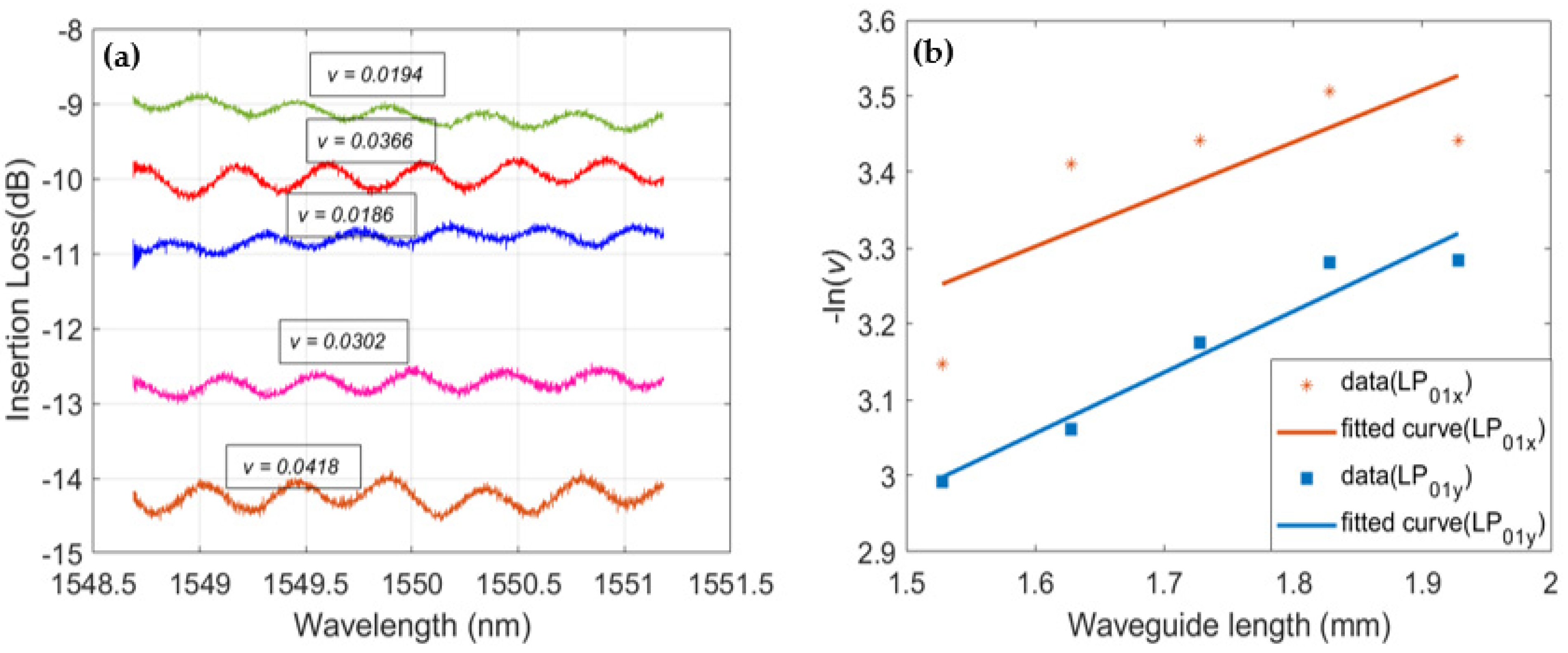
In attempt to obtain a better propagation loss estimation, we designed a second-generation waveguide with significant propagation length at a constant core diameter of 2 μm. Working around the writing footprint limit of Nanoscribe and capitalizing on the 3D nature of DLW, we designed a folded waveguide following a rectangular spiral geometry, with the inner waveguide end exiting the structure by being bent upwards and passing over the spiral waveguides (Figure 10). Five different waveguide lengths were printed, all with the same upward-bending ends for coupling, and with twelve 90° bends of 25 μm radius (making three spiral revolutions at a 10 μm waveguide pitch), with varying lengths of the straight segments. The overall waveguide lengths following this design were mm, and five identical copies of each waveguide length were printed. All 25 waveguides were identically analyzed by coupling with lensed fibers oriented at 45° and performing a spectral scan with the optical vector analyzer.
Unfortunately, the loss variation for each identical design persisted. We measured the same structure multiple times and found that the insertion loss values were consistently nearly equal for the same waveguide structure. Figure 11a shows the five spectral scans for the 1.728 mm long waveguide, with losses varying from 9 dB down to 14.5 dB. Such large loss variations for identical waveguides are likely due to either coupling in/out loss variations or random waveguide defects/roughness that are unique to each printed sample. We resorted to the fringe visibility analysis technique, as it is independent of the coupling losses (an internal waveguide cavity process), and attached a fringe visibility value, , to each trace (see inset values next to each trace). The fringe visibility values continued to show large variations, indicating that printed defects/roughness were present. (We assumed that end-facet reflection variations were contributing to a lesser degree, since we significantly lengthened the waveguides.) For our loss analysis, we adopted the largest fringe visibility value of the five printed waveguides of identical length, as it represents the waveguide sample that had the fewest printing defects, and hence we obtained a ‘best value’ for each of the five waveguide lengths. The longer waveguides also allowed us to assess the waveguide’s group index more accurately: with an FSR of 0.4 nm +/−0.006 nm for the 1.928 mm long waveguide, we obtained an estimated value for of 1.55.
We can now estimate the waveguide propagation loss more accurately, by fitting a trend line relating the reduction in fringe visibility (due to increased cavity losses attributed to propagation losses) to the waveguide length (Figure 11b). The relationship between propagation loss, a, waveguide length, L, end-facet reflection, R, and fringe visibility, , is given by (detailed derivation in the Appendix A):
Equation (3) indicates that if we plot the measured term for the different waveguide lengths, then the slope of the regression line will measure the propagation loss and the intercept of the curve at zero length will provide the end reflection. Using this technique, we found propagation loss values of 2.9 dB/mm and 3.4 dB/mm for the LP01x and LP01y polarizations, respectively (the OVA presents the principal modes without distinguishing them. We ascribe the higher loss polarization of the LP01y mode to the impact of the nano-fin). The end-facet reflection values were 0.055 and 0.08 for the LP01x and LP01y polarizations, respectively. These estimated values of Fresnel reflections were slightly high, but within the right range.
We attribute the high propagation losses to the roughness of side wall of the waveguide, as shown in Figure 8c. Propagation losses due to surface roughness scale with core–cladding index contrast and mode intensity at the core–cladding interface [28]. For air-cladded nano-fabricated waveguides, these two contributing factors are high, which is the likely cause of our relatively high propagation loss values. However, since the overall length of these waveguides are envisaged to be short, the main loss contributor will originate from external coupling, which can be better optimized.
5. Conclusions
We built and characterized air-cladded single-mode polymer optical waveguides, fabricated by means of direct laser writing, and supported by a narrow fin which has a minimal impact on optical performance. Coupling in and out of the waveguides was aided by bending both ends upwards at 45° from the substrate to facilitate lensed fiber alignment. Waveguides of two-micron diameter, with lengths from hundreds of microns to a couple of millimeters, were printed, all proving to be robust and functional due to the stability afforded by the nano-fin support to the substrate. This waveguide design opens new possibilities for interconnection and sensing devices for various applications. Free-standing waveguides are exposed to the surrounding area, which enhances the interaction of the evanescent field of the guided mode with the external sensing medium, offering new prospects for the design of highly sensitive sensors. TPP-based devices can also be fabricated directly on a fiber tip and can help realize single-fiber-based sensors for various applications.
Author Contributions
P.K.G. designed and fabricated waveguides and performed the experiments; D.M.M. discussed and gave suggestions on the design and experiments; P.K.G. wrote the paper, and D.M.M. revised and edited the paper. Both authors have read and agreed to the published version of the manuscript.
Funding
This work is funded in part by the Pazy Foundation and by the Israel Ministry of Science.
Acknowledgments
We thank Yehudit Garcia (Peter Brojde Center for Innovative Engineering at the Hebrew University of Jerusalem) for her guidance on the Nanoscribe system during the waveguide fabrication process, and Aleksey Kukin (Photonic Devices Lab, The Hebrew University of Jerusalem) for his help in designing the experimental setup for characterizing the fabricated waveguides in our laboratory.
Conflicts of Interest
The authors declare no conflict of interest.
Appendix A
To assess the propagation loss of printed waveguide samples of different lengths, having supposedly common loss factors, such as coupling and end-facet reflections, we slightly modified the fringe contrast analysis technique of [29,30] by introducing the fringe visibility metric, and separated the different contributions of the Fabry–Perot etalon due to the waveguide end-facet reflections. The normalized output intensity of the etalon is provided by:
Here, is the transmitted intensity and is the input intensity (or powers), R is the Fresnel intensity reflection at the two end facets (under the relevant assumption that they are equal), is the transmission efficiency via the waveguide of length L and loss a (per unit length), and φ is the cavity phase delay. The Fabry–Perot transmission curve has distinct maximum or minimum values, at wavelengths where the cavity phase delay is interfered constructively or destructively (depending on the term being zero or one), hence:
The oscillatory transmission curve exhibiting the interference effect is normally characterized with the dimensionless visibility metric, , defined as:
Since and (certainly for waveguide materials with ), then . We can now separate the propagation and reflection contributions:
Applying a natural logarithm and simplifying, we have:
Equation (A5) is a linear curve relating the waveguide length to the observed visibility, with two unknowns that can be estimated using regression analysis: the slope, or loss, , and the offset, or Fresnel reflection, .
References
- Joe, H.-E.; Yun, H.; Jo, S.H.; Jun, M.B.; Min, B.K. A Review on Optical Fiber Sensors for Environmental Monitoring. Int. J. Precis. Eng. Manuf. Green Technol. 2018, 5, 173–191. [Google Scholar] [CrossRef]
- Horváth, R.; Pedersen, H.C.; Skivesen, N.; Selmeczi, D.; Larsen, N.B. Optical waveguide sensor for on-line monitoring of bacteria. Opt. Lett. 2003, 28, 1233–1235. [Google Scholar] [CrossRef] [Green Version]
- Kaur, P.; Shenoy, M. Highly Sensitive Refractive Index Sensor based on Silicon Nitride Strip Waveguide Directional Coupler. IEEE Sens. Lett. 2018, 2, 3500504. [Google Scholar] [CrossRef]
- Qian, Y.; Zhao, Y.; Wu, Q.L.; Yang, Y. Review of salinity measurement technology based on optical fiber sensor. Sens. Actuators B Chem. 2018, 260, 86–105. [Google Scholar] [CrossRef]
- Willer, U. Fiber-optic evanescent-field laser sensor for in-situ gas diagnostics. Spectrochim. Acta Part A Mol. Biomol. Spectrosc. 2002, 58, 2427–2432. [Google Scholar] [CrossRef]
- Schmitt, K.; Schirmer, B.; Hoffmann, C.; Brandenburg, A.; Meyrueis, P. Interferometric biosensor based on planar optical waveguide sensor chips for label-free detection of surface bound bioreactions. Biosens. Bioelectron. 2007, 22, 2591–2597. [Google Scholar] [CrossRef]
- Knoerzer, M.; Szydzik, C.; Ren, G.; Huertas, C.S.; Palmer, S.; Tang, P.; Nguyen, T.G.; Bui, L.; Boes, A.; Mitchell, A. Optical frequency comb based system for photonic refractive index sensor interrogation. Opt. Express 2019, 27, 21532. [Google Scholar] [CrossRef]
- Soler, M.; Huertas, C.S.; Lechuga, L.M. Label-free plasmonic biosensors for point-of-care diagnostics: A review. Expert Rev. Mol. Diagn. 2019, 19, 71–81. [Google Scholar] [CrossRef]
- Xu, F.; Brambilla, G. Demonstration of a refractometric sensor based on optical microfiber coil resonator. Appl. Phys. Lett. 2008, 92, 101126. [Google Scholar] [CrossRef] [Green Version]
- Sumetsky, M.; Dulashko, Y.; Fini, J.M.; Hale, A.; DiGiovanni, D.J. The Microfiber Loop Resonator: Theory, Experiment, and Application. J. Lightwave Technol. 2006, 24, 242–250. [Google Scholar] [CrossRef]
- Vlk, M.; Datta, A.; Alberti, S.; Yallew, H.D.; Mittal, V.; Murugan, G.S.; Jágerská, J. Extraordinary evanescent field confinement waveguide sensor for mid-infrared trace gas spectroscopy. Light Sci Appl. 2021, 10, 26. [Google Scholar] [CrossRef] [PubMed]
- Vollmer, F.; Yang, L. Label-free detection with high-Q microcavities: A review of biosensing mechanisms for integrated devices. Nanophotonics 2012, 1, 267–291. [Google Scholar] [CrossRef] [PubMed] [Green Version]
- Zou, Y.; Chakravarty, S.; Chung, C.J.; Xu, X.; Chen, R.T. Mid-infrared silicon photonic waveguides and devices. Photonics Res. 2018, 6, 254–276. [Google Scholar] [CrossRef]
- Swargiary, K.; Jarutatsanangkoon, P.; Suwanich, P.; Jolivot, R.; Mohammed, W.S. Single-step 3D-printed integrated optical system and its implementation for a sensing application using digital light processing technology. Appl. Opt. 2020, 59, 122–128. [Google Scholar] [CrossRef]
- Gross, A.J.; Bertoldi, K. Additive Manufacturing of Nanostructures That Are Delicate, Complex, and Smaller than Ever. Small 2019, 15, 1–6. [Google Scholar] [CrossRef] [PubMed]
- Serbin, J.; Ovsianikov, A.; Chichkov, B. Fabrication of woodpile structures by two-photon polymerization and investigation of their optical properties. Opt. Express 2004, 12, 5221–5228. [Google Scholar] [CrossRef] [Green Version]
- Frenzel, T.; Kadic, M.; Wegner, M. Three dimensional mechanical metamaterials with a twist. Science 2017, 358, 1072–1074. [Google Scholar] [CrossRef] [Green Version]
- Bückmann, T.; Stenger, N.; Kadic, M.; Kaschke, J.; Frölich, A.; Kennerknecht, T.; Wegener, M. Tailored 3D Mechanical Metamaterials Made by Dip-in Direct-Laser-Writing Optical Lithography. Adv. Mater. 2012, 24, 2710–2714. [Google Scholar] [CrossRef]
- Gale, B.K.; Jafek, A.R.; Lambert, C.J.; Goenner, B.L.; Moghimifam, H.; Nze, U.C.; Kamarapu, S.K. A Review of Current Methods in Microfluidic Device Fabrication and Future Commercialization Prospects. Inventions 2018, 3, 60. [Google Scholar] [CrossRef] [Green Version]
- Schmid, M.; Thiele, S.; Herkommer, A.; Giessen, H. Three-dimensional direct laser written achromatic axicons and multi-component microlenses. Opt. Lett. 2018, 43, 5837. [Google Scholar] [CrossRef]
- West, H.; Garcia, Y.; Rechtman, L.; Blau, M.; Marom, D.M. Subwavelength Nano-Pyramids 3D Printed Directly on Optical Fiber Tip Serving as Anti-Reflection Coating. In Proceedings of the 2018 International Conference on Optical MEMS and Nanophotonics (OMN), Lausanne, Switzerland, 29 July–2 August 2018; pp. 1–5. [Google Scholar]
- Lindenmann, N.; Balthasar, G.; Hillerkuss, D.; Schmogrow, R.; Jordan, M.; Leuthold, J.; Koos, C. Photonic wire bonding: A novel concept for chip-scale interconnects. Opt. Express 2012, 20, 17667. [Google Scholar] [CrossRef] [Green Version]
- Vanmol, K.; Saurav, K.; Panapakkam, V.; Thienpont, H.; Vermeulen, N.; Watté, J.; Van Erps, J. Mode-field matching down-Tapers on single-mode optical fibers for edge coupling towards generic photonic integrated circuit platforms. J. Lightwave Technol. 2020, 38, 4834–4842. [Google Scholar] [CrossRef]
- Gao, H.; Chen, G.F.; Xing, P.; Choi, J.W.; Low, H.Y.; Tan, D.T. High-Resolution 3D Printed Photonic Waveguide Devices. Adv. Opt. Mater. 2020, 8, 2000613. [Google Scholar] [CrossRef]
- Schmid, M.; Ludescher, D.; Giessen, H. Optical properties of photoresists for femtosecond 3D printing: Refractive index, extinction, luminescence-dose dependence, aging, heat treatment and comparison between 1-photon and 2-photon exposure. Opt. Mater. Express 2019, 9, 4564. [Google Scholar] [CrossRef]
- Brimont, A.; Hu, X.; Cueff, S.; Romeo, P.R.; Saint Girons, G.; Griol, A.; Orobtchouk, R. Low-Loss and compact silicon rib waveguide bends. IEEE Photonics Technol. Lett. 2016, 28, 299–302. [Google Scholar] [CrossRef] [Green Version]
- 3M Company. 3M™ Novec™ 7100 Engineered Fluid; 3M Company: St. Paul, MN, USA, 2020; Available online: http://multimedia.2m.com.mediawebserver (accessed on 3 July 2021).
- Shi, Y.; Ma, L.; Zhuang, Y.; He, Z. Investigation on roughness-induced scattering loss of small-core polymer waveguides for single-mode optical interconnect applications. Opt. Express 2020, 28, 38733. [Google Scholar] [CrossRef] [PubMed]
- Regener, R.; Sohler, W. Loss in low-finesse Ti:LiNbO3 optical waveguide resonators. Appl. Phys. B 1985, 36, 143–147. [Google Scholar] [CrossRef]
- Taebi, S.; Khorasaninejad, M.; Saini, S.S. Modified Fabry-Perot interferometric method for waveguide loss measurement. Appl. Opt. 2008, 47, 6625–6630. [Google Scholar] [CrossRef]
Figure 1.
Simulated mode field profiles of nano-fin supported, single mode waveguides (vertically polarized) for core diameters of (a) 1.6 μm, (b) 1.9 μm, and (c) 2.2 μm. The ability to fabricate such structures is demonstrated in the cross-section image of our fabricated waveguide (after FIB sectioning, shown in (d)), viewed at a 52° tilt from vertical.

Figure 2.
(a) Cross-section of the single mode waveguide supported by a nano-fin to the substrate, demonstrating the waveguide definitions of its diameter, d, fin height, h, and nano-fin width, w. (b) Variation of the guided modes’ effective indices at different core diameters for a free-standing waveguide, with and without the fin support.
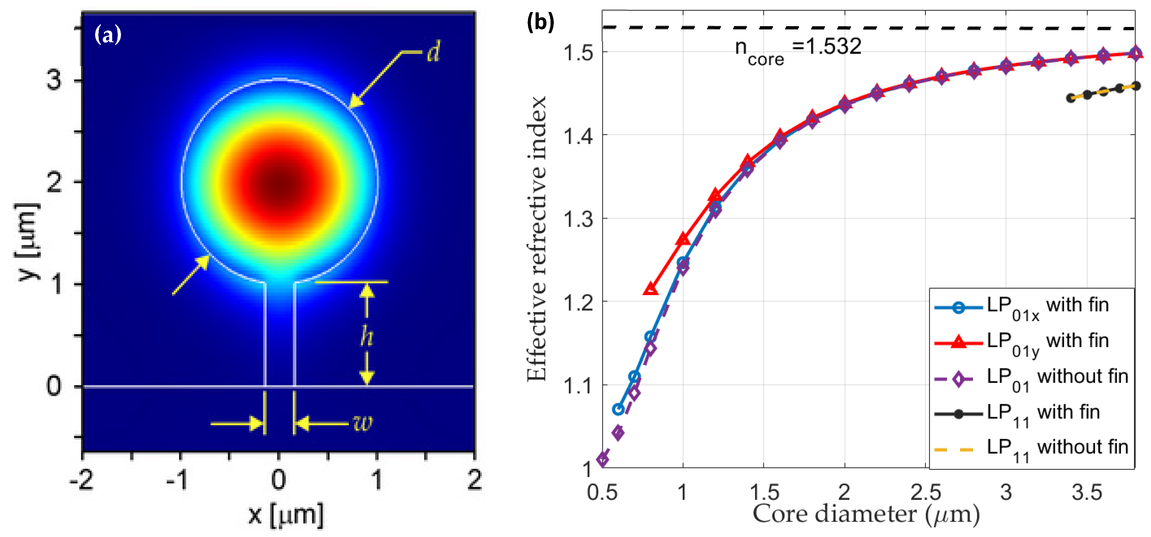
Figure 3.
(a) Effective refractive index variation with fin height, h, for fin width of 0.3 μm. (b) Effective refractive index variation with fin width, w, for fin height of 1.5 μm and core diameters of 1.5 and 2 μm, for LP01x and LP01y modes.
Figure 3.
(a) Effective refractive index variation with fin height, h, for fin width of 0.3 μm. (b) Effective refractive index variation with fin width, w, for fin height of 1.5 μm and core diameters of 1.5 and 2 μm, for LP01x and LP01y modes.
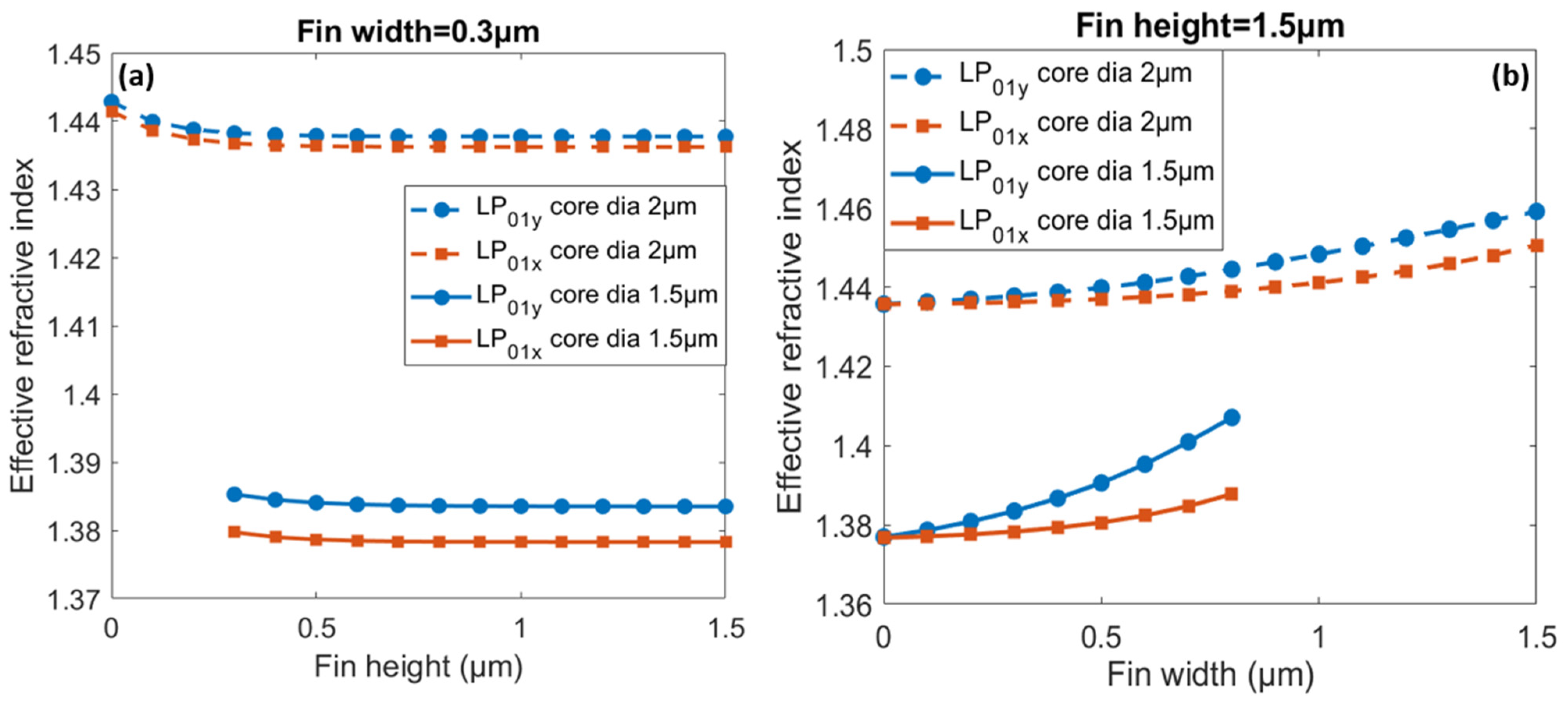
Figure 4.
(a) Top view of the electric field modulus propagation through three 90° bent waveguides of 2 μm diameter, with bend radii of 5, 10, and 15 µm (composite view, separated by hatched pattern). (b) Bend loss as a function of bend radius for waveguide diameters of 1.5 and 2 μm, with and without nano-fin support. Insets show intensity profiles in bent waveguides of radius 5, 15, and 25 μm.

Figure 5.
(a) Electric field propagation through the tapered waveguide, evolving from a 2 µm to a 4 μm diameter within ~80 μm. (b) Output mode coupling efficiency to the fundamental LP01 and higher-order LP02 modes, as a function of taper length.
Figure 5.
(a) Electric field propagation through the tapered waveguide, evolving from a 2 µm to a 4 μm diameter within ~80 μm. (b) Output mode coupling efficiency to the fundamental LP01 and higher-order LP02 modes, as a function of taper length.
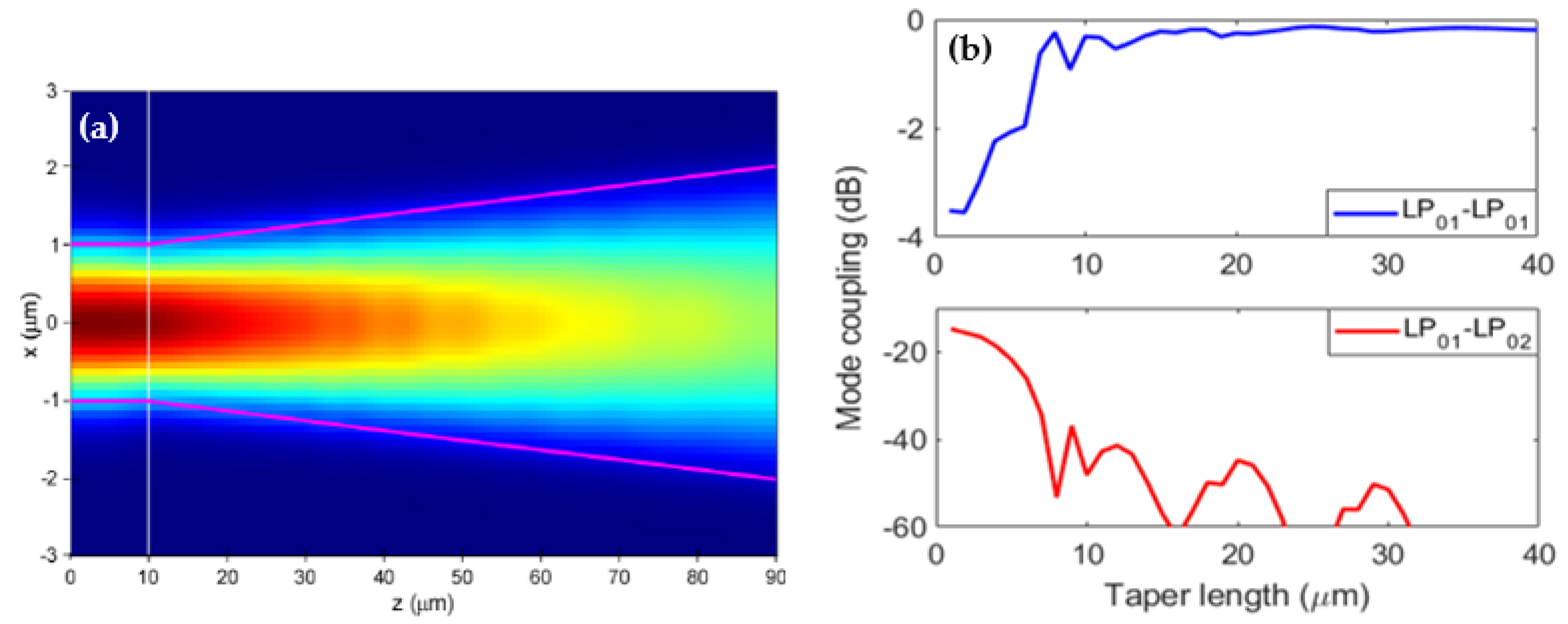
Figure 6.
Variation of the confinement factor inside the core with and without a fin of 1.5 μm height.
Figure 6.
Variation of the confinement factor inside the core with and without a fin of 1.5 μm height.
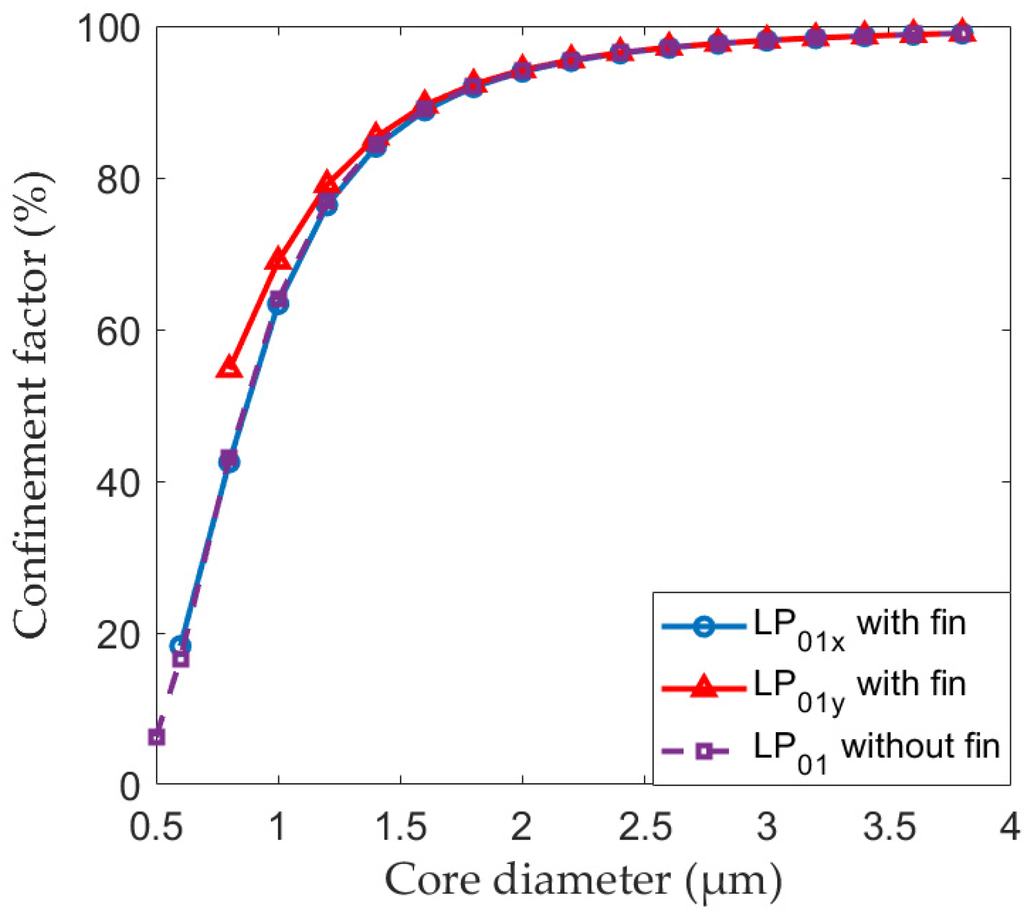
Figure 7.
(a) Isometric view of 3D waveguide design in software. (b) HRSEM image of fabricated waveguide supported by the nano-fin.
Figure 7.
(a) Isometric view of 3D waveguide design in software. (b) HRSEM image of fabricated waveguide supported by the nano-fin.

Figure 8.
(a) Fabricated spiral waveguide, in the process of scanning with AFM tip, (b) AFM image of the waveguide’s curved surface topography, and (c) two line profiles along waveguide direction revealing its surface roughness.
Figure 8.
(a) Fabricated spiral waveguide, in the process of scanning with AFM tip, (b) AFM image of the waveguide’s curved surface topography, and (c) two line profiles along waveguide direction revealing its surface roughness.
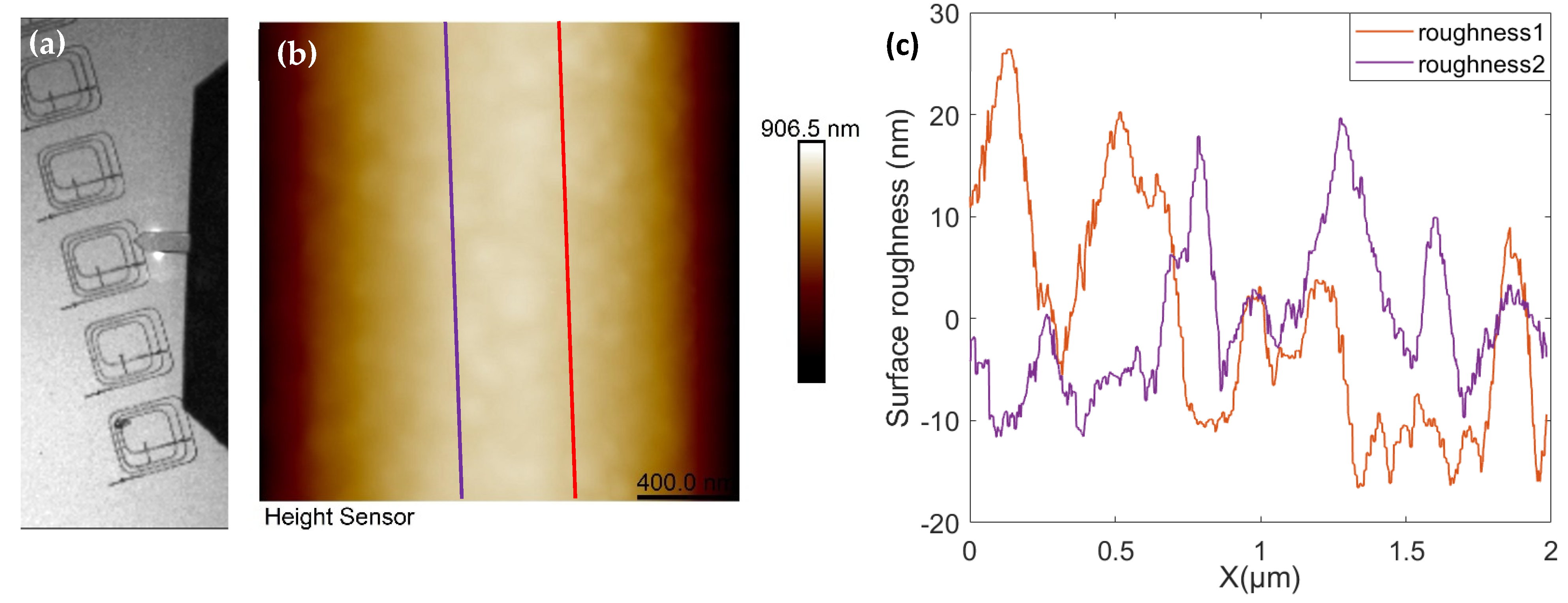
Figure 9.
(a) Experimental setup to couple to the waveguides using lensed fibers, with magnified view of the lensed fiber coupling on the left. (b) Transmission spectrum of printed waveguide for the two principle polarization states.
Figure 9.
(a) Experimental setup to couple to the waveguides using lensed fibers, with magnified view of the lensed fiber coupling on the left. (b) Transmission spectrum of printed waveguide for the two principle polarization states.
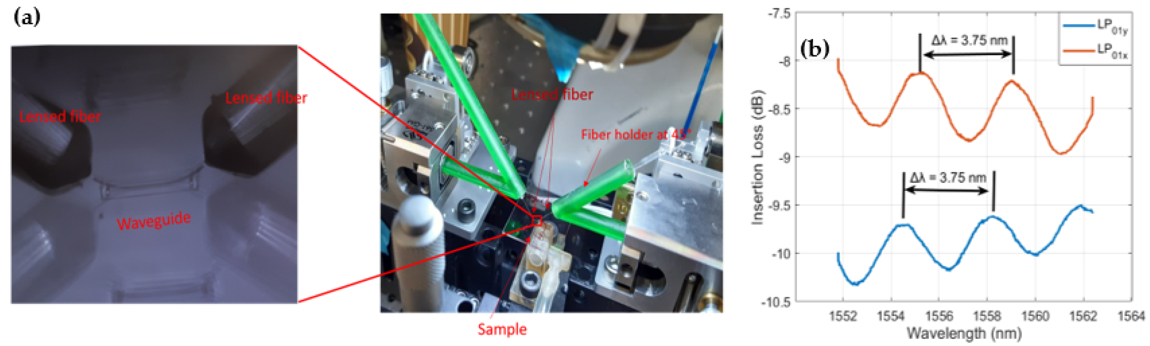
Figure 10.
(a) HRSEM image of the fabricated spiral waveguide, consisting of four fabricated waveguide structures in parallel. (b) HRSEM image of the spiral-shaped waveguide, supported with a narrow fin.
Figure 10.
(a) HRSEM image of the fabricated spiral waveguide, consisting of four fabricated waveguide structures in parallel. (b) HRSEM image of the spiral-shaped waveguide, supported with a narrow fin.

Figure 11.
(a) Measured insertion loss variation of five identical waveguide samples of equal total length (1728 μm). (b) Loss regression analysis for estimation of waveguide propagation loss.
Figure 11.
(a) Measured insertion loss variation of five identical waveguide samples of equal total length (1728 μm). (b) Loss regression analysis for estimation of waveguide propagation loss.
Publisher’s Note: MDPI stays neutral with regard to jurisdictional claims in published maps and institutional affiliations. |
© 2021 by the authors. Licensee MDPI, Basel, Switzerland. This article is an open access article distributed under the terms and conditions of the Creative Commons Attribution (CC BY) license (https://creativecommons.org/licenses/by/4.0/).
Share and Cite
MDPI and ACS Style
Gill, P.K.; Marom, D.M. Single Mode, Air-Cladded Optical Waveguides Supported by a Nano-Fin Fabricated with Direct Laser Writing. Appl. Sci. 2021, 11, 6327. https://doi.org/10.3390/app11146327
AMA Style
Gill PK, Marom DM. Single Mode, Air-Cladded Optical Waveguides Supported by a Nano-Fin Fabricated with Direct Laser Writing. Applied Sciences. 2021; 11(14):6327. https://doi.org/10.3390/app11146327
Chicago/Turabian StyleGill, Parvinder K., and Dan M. Marom. 2021. "Single Mode, Air-Cladded Optical Waveguides Supported by a Nano-Fin Fabricated with Direct Laser Writing" Applied Sciences 11, no. 14: 6327. https://doi.org/10.3390/app11146327
Note that from the first issue of 2016, this journal uses article numbers instead of page numbers. See further details here.