
Formal Chaos Existing Conditions on a Transmission Line Circuit with a Piecewise Linear Resistor


1
Graduate School of Electrical and Information Engineering, Shonan Institute of Technology, 1-1-25 Tsujido Nishikaigan, Fujisawa 251-8511, Japan
2
Private Consultant, Fujisawa 251-8511, Japan
*
Author to whom correspondence should be addressed.
Appl. Sci. 2021, 11(20), 9672; https://doi.org/10.3390/app11209672
Submission received: 1 September 2021
/
Revised: 11 October 2021
/
Accepted: 12 October 2021
/
Published: 17 October 2021
Abstract
:By using one-dimensional (1-D) map methods, some lossless transmission line circuits with a short at one side terminal have been actively studied. Bifurcation results or chaotic states in the circuits have been reported. On the other hand, many weak or strong definitions such that a 1-D map is mathematically chaotic are still being studied. In such definitions, the definition of formal chaos is well known as being the most traditional and most definite. However, formal chaos existences have not been rigorously proven in such circuits. In this paper, a general lossless transmission circuit is considered first with a dc bias voltage source in series with a load resistor at one side terminal and with a three-segment piecewise linear resistor at another side terminal. Secondly, the method for deriving a 1-D map describing the behavior of the circuit is summarized. Thirdly, to provide a basis of chaotic application for the 1-D map, the mathematical definition of formal chaos and the sufficient conditions of the existence of formal chaos are discussed. Furthermore, by using Maple, formal chaos existences and bifurcation behavior of 1-D maps are presented. By using the Lyapunov exponent, the observability of formal chaos in such bifurcation processes is outlined. Finally, the principal results and the future works are summarized.
1. Introduction
Transmission line circuits, switched capacitor circuits, neuron model circuits, and constrained circuits are notable as the nonlinear circuits of which behavior may be described by one-dimensional (1-D) maps [1,2,3,4,5,6,7,8,9,10,11]. Furthermore, in [12], by using real imperfect integrated devices induced by unavoidable manufacturing imperfections that plausibly have so called hidden dynamics with parasitic effects and nonidealities, the possibility of designing imperfect electronic circuits generating megahertz chaotic oscillations, without the use of additional capacitors or inductors, has been explored and discussed.
By using one-dimensional (1-D) map methods, some lossless transmission line circuits with a short at one side terminal [5,6,7,8,9,10,11] (or, with a dc bias voltage source in series with a load resistor at one side terminal [7]) have been actively studied. On the other hand, many weak or strong definitions such that a 1-D map is mathematically chaotic are still being studied [13,14,15,16,17,18]. In this paper, we use the following definition that is well known as most traditional and most definite since Moser [19].
Definition 1.
A 1-D discrete dynamical system or 1-D map φ on M is said to be chaotic if there exists an invariant subseton which some iterates of φ is topologically conjugate to the shift dynamicswith m symbols.
The shift dynamics with m symbols has the following properties [13,15,16,17]: (1) There are countably many periodic points with different periods in . (2) The set of all periodic points in dense in . (3) is topologically transitive. Namely, there exists a point where its orbit is dense in . (4) is topologically expansive. (5) is homeomorphic to a Cantor set. (6) The topological entropy of is .
For a 1-D discrete dynamical system , it is well known that “φ has a homoclinic point” implies Definition 1, and they are often equivalent [15,20,21]. Definition 1 is not based on the theoretical measure but is based on the topological viewpoint, and it is called formal chaos or topological chaos, which may be not observable generally [13]. Thus, we call the chaos in Definition 1 formal chaos.
Binary sequences based on observable chaotic behavior produced by 1-D maps coming from the nonlinear circuits are reported and well known to have good statistical properties useful for applications relative to several digital communication systems [4,13]. However, the sufficient conditions for the existence of observable chaos are so strong that most 1-D maps coming from general nonlinear circuits cannot be rigorously proved to possess observable chaos. Indeed, for general 1-D maps such that the absolute slops of them are either greater or less than unity, it is very difficult to rigourously prove the existence of observable chaos, except for 1-D maps such as the logistic map family or 1-D piecewise linear maps such that all their absolute slopes of are greater than unity.
Once the existence of formal chaos is guaranteed, the degree of the observability of the chaos can be checked by the existence of maximal positive Lyapunov exponent [14] through computer simulations from the viewpoint of engineering. Hence, we pay attention to the sufficient condition that formal chaos in Definition 1 exists in a 1-D map.
In [5,6], a lossless transmission line circuit with a short at one side terminal and with a three-segment piecewise linear (3SPWL) resistor (so called Nagumo’s 3SPWL resistor) at another side terminal is considered. The characteristic of the (3SPWL) resistor is not only in point symmetry at the origin but also in all four quadrants of a coordinate system. The method for deriving a 1-D map describing the dynamics of the circuit is discussed at the base of the incident and reflected waves. Some analytical results are obtained by using the 1-D map. In [8,9,10], for a lossless transmission line circuit with a short at one side terminal and with a three-segment piecewise linear resistor function at another side terminal, the conditions are provided for the existence of the explicit function form of the incident and reflected wave transformed from the three-segment piecewise linear resistor function, the existence of the 1-D map, and the existence of the invariant interval of the 1-D map. Furthermore, in [8,9,10,11], by using a 1-D map, analytical bifurcation results or chaotic states (except for formal chaos) are reported in terms of numerical simulation.
However, formal chaos and observable chaos existence [13,18,20] have not been rigorously proven in such lossless transmission line circuits in [5,6,7,8,9,10,11]. In [22], by using interval arithmetic, the formal chaos existence was proven in a lossless transmission line circuit, but the proof is very tedious.
In this paper, from the above background, in Section 2, we consider a lossless transmission circuit with a dc bias voltage source in series with a load resistor at one side terminal and with a three-segment piecewise linear resistor at another side terminal. In Section 3, we summarize the method for deriving a 1-D map describing the behavior of the circuit. In Section 4, in order to provide a basis of chaotic application for the 1-D map (or the transmission circuit), we discuss the mathematical definition of formal chaos and the sufficient conditions of the existence of formal chaos for generating 1-D maps. In Section 5, using Maple [23], we present an example of formal chaos existence and several examples of bifurcation behavior of 1-D maps. Using the degree of observability of chaotic states in terms of Lyapunov exponent, we discuss the observability of formal chaos in such bifurcation processes. In the Conclusion section, we summarize the principal results and the future works. In particular, we mention the possibility of designing imperfect transmission lines with parasitic effects and nonidealities inside real integrated devices generating high frequency ranges and chaotic oscillations without the use of additional capacitors or inductors.
2. Lossless Transmission Circuit Equations with Terminal Conditions
Incorporating the works in [5,6,7,8,9,10], we consider a lossless transmission circuit with a dc bias voltage source in series with a load resistor at one side terminal and with a three-segment piecewise linear resistor at another side terminal such as (N) Nagumo’s 3SPWL resistor in Figure 1 and Figure 2 or (T) the present authors’ Modeled Tunnel Diode (TD) 3SPWL resistor in Figure 3 and Figure 4 in Figure 5. The circuit in Figure 5 can be represented by the circuit in Figure 6 with 3SPWL resistor (N) or (T) together with the side terminal conditions as follows. At one side terminal A of the circuit, we have the following: (i) a dc bias voltage source in series with 3SPWL resistor (N) or (T): ; and (ii) 3SPWL resistor (N) or (T): . At another side terminal B of the circuit, we have the following: (1) short: , ; (2) open: , ; (3) a load resistor: , ; (4) a dc bias voltage source: , ; or (5) a dc bias voltage source in series with a load resistor: , . We focus on considering a lossless transmission line circuit with 3SPWL resistor (N) or (T), together with the above side terminal conditions in Figure 6.
2.1. Three-Segment Piecewise Linear Resistor
The three-segment Piecewise Linear (3SPWL) resistor , in Figure 5 is realized by the op amp based circuit (N) Nagumo’s 3SPWL resistor in Figure 1 and Figure 2 or (T) the present authors’ Modeled Tunnel Diode (TD) 3SPWL resistor in Figure 3 and Figure 4. In Figure 1 or Figure 3, (or ) denotes positive (or negative) saturation of the op amp, and (or ) denotes positive (or negative) power supply. in Figure 3 denotes the forward voltage drop of the ideal switching diode. In Figure 2 or Figure 4, the v-i characteristic of is always of the N type such that , , and are positive, negative, and positive slopes, respectively.
(N) Nagumo’s 3SPWL Resistor :
The slopes , and break points and in Figure 2 are given as follows:
on the condition that , , , and . is freely set up by . (i.e., ) is also freely set up by because, for any op amps, (or ) is generally in proportion to (or ).
(T) TD 3SPWL Resistor :
The slopes , and break points and in Figure 4 are given as follows:
on the conditions that , , , , and . is freely set up by . (i.e., ) is also freely set up by because, for any op amps, is generally in proportion to .
2.2. Transmission Line Circuit Equation
The relation of the voltage v and the current i in the line in Figure 6 becomes the following:
where is the characteristic impedance of the line; is the propagation velocity of waves in the line; , , , , , L are the series of inductance per unit length of the line; C is the parallel capacitance per unit length of the line; l is line length; is the voltage in the line; is the current in the line; is the coordinate in the line; v is the non-dimensional voltage in the line; i is the non-dimensional current in the line; x is the non-dimensional coordinate in the line; and is non-dimensional time. Accordingly, by eliminating i (or v), we have the following.
The following Equations (3) and (4) provide the boundary conditions of Figure 6. Equations (3) and (4) also provide the boundary conditions of Figure 5 as follows. At one side terminal, we have the following: (i) a dc bias voltage source in series with 3SPWL resistor (N) or (T): and (ii) 3SPWL resistor (N) or (T): . At another side terminal, we have the following: (1) short: , ; (2) open: , ; (3) a load resistor: , ; (4) a dc bias voltage source: , ; or (5) a dc bias voltage source in series with a load resistor: , .
(N) Nagumo’s 3SPWL Resistor :
Here, , , , , .
(T) TD 3SPWL Resistor :
Here, , , ,, . In addition in (N) or (T), , , , , , and are the dc bias voltage sources; is the load resistor; and is the non-dimensional current of 3SPWL resistor, .
3. 1-D Map Describing the Behavior of the Transmission Line Circuit
3.1. Derivation of 1-D Map
Here, we discuss how to derive the 1-D map or the difference equation of which the dynamics completely describes the dynamics of Equations (2)–(6).
The 1-D wave equation of Equation (2) has the d’Alembert’s solution, which is described as the following.
Equation (7) can be solved with regard to the scattering variables, that is, and . Then, we have the following description.
Equation (8) denotes that the -coordinate system is identical with the rotation of -coordinate system. Substituting Equation (7) into Equations (3) and (4), we rewrite the boundary conditions as follows:
where the time is shifted back in (10) and .
The following Equations (9) and (10) provide the boundary conditions of Figure 6. Equations (9) and (10) also provide the boundary conditions of Figure 5 as follows.
At one side terminal, we have the following: (i) a dc bias voltage source in series with 3SPWL resistor (N) or (T): and (ii) 3SPWL resistor (N) or (T): . At another side terminal, we have the following: (1) short: , ; (2) open: , ; (3) a load resistor: , ; (4) a dc bias voltage source: , ; or (5) a dc bias voltage source in series with a load resistor: , .
Since is a three segment piecewise linear function, we can identify Equation (11) with for , :
where and .
Here, from Equations (9) and (10), we briefly show how to derive an explicit piecewise linear 1-D map of and . First of all, substitute Equation (11) into at the right hand side of Equation (10). We obtain Equations (12) and (13). Now since Equations (9) and (12) are simultaneous linear equations, we solve Equations (9) and (12) as Equation (14). We also solve Equations (12) and (13) as Equation (15).
In the following, using the similar procedure from Equations (9)–(15), we provide Theorem 1 and Corollary 1 such that and are explicitly determined by 1-D maps of with the iterative time 1. We also provide Corollary 2 such that is explicitly determined by the1-D map of .
Theorem 1.
If and Nagumo’s 3SPWL Resistor is or TD 3SPWL Resistor is , then , : is defined by the following:
which also holds when the following is the case:
or we have the following:
where is the slope of , , and is the set of real numbers.
Proof in Appendix A.
Corollary 1.
If and Nagumo’s 3SPWL Resistor is or TD 3SPWL Resistor is , then , : is defined by the following:
in the case where : , , holds, where : slope of , .
The other case is where : , , holds, where is the − slope of , , and is the set of real numbers.
Proof in Appendix A.
Corollary 2.
If and Nagumo’s 3SPWL Resistor is or TD 3SPWL Resistor is , then is explicitly determined by 1-D map of such that the following is the case.
Remark that , for any τ.
Proof in Appendix A.
3.2. Global Behavior of 1-D Map
Here, we provide Theorem 2 to guarantee that for any initial point, every orbit by the iteration of the 1-D map of ultimately penetrates an invariant interval set.
Theorem 2.
If , and Nagumo’s 3SPWL Resistor : , , and or TD 3SPWL Resistor : , , and , then the following is the case.
- The 1-D map has a unique unstable fixed point in the interval , where,.
- There exists an invariant interval such that and , where ,,,.
- For any , there exists jth iterate of such that , where denotes the jth iterate of , i.e., is the j-fold composition of with itself. is the set of non negative integers.
Proof in Appendix A.
4. Formal Chaos Existing Conditions of 1-D Maps
As mentioned before, binary sequences based on observable chaotic behavior produced by 1-D maps are well known to have good statistical properties useful for applications relative to several digital communication systems [4,13]. However, the sufficient conditions for the existence of observable chaos are so strong that most 1-D maps cannot be rigorously proved to possess observable chaos. Furthermore, once the existence of formal chaos is guaranteed, the degree of the observability of the chaos can be checked by the existence of maximal positive Lyapunov exponent [14] through computer simulations from the viewpoint of engineering. Hence, we focus on the sufficient condition that formal chaos in Definition 1 exists in a 1-D map.
4.1. Formal Chaos Existing Conditions of a General 1-D Map
In this subsection, in order to verify formal chaos existence for 1-D map easily, we provide Theorem 3 to guarantee the formal chaos existence in Definition 1 in the case of . Although a similar 1-D map to the map in Theorem 3 appears in Devaney or Aoki’s mathematical proof process for “ has a homoclinic point” implying Definition 1 in [15,21], the existence of the similar 1-D map has not been considered as an easy-to-use sufficient condition implying Definition 1.
Therefore, the authors propose to adopt the existence of the similar 1-D map as the sufficient condition implying Definition 1 and to summarize this condition as Theorem 3. This theorem can be regarded as 1-D map version of Moser’s theorems [14,19] for two dimensional maps.
Theorem 3.
Let I be a closed interval of real numbers. Let f be a continuous piecewise differentiable mapping from I to itself and be a derivative of f.
- There exist and disjoint closed subintervals in I such that and .
- holds for any x in . If f satisfies and , then the invariant set exists, and the 1-D map f on Λ is topologically conjugate to the shift dynamics with 2 symbols. The one-dimensional map f on Λ is mathematically chaotic.
Proof in Appendix A.
4.2. Formal Chaos Existing Conditions of a 1-D Map Family
As mentioned precisely in the later subsections, for a lossless transmission circuit with a dc bias voltage source in series with a load resistor at one side terminal and with a three-segment piecewise linear resistor at another side terminal, the existence of a three-segment piecewise linear 1-D map describing the dynamics of the circuit, the existence of the invariant interval of the 1-D map, and the coordinate transformation from the invariant interval to the normalized interval are provided.
Therefore, in this subsection, we pay our attention to the normalized 1-D map on the normalized interval I after applying the coordinate transformation to the three-segment piecewise linear 1-D map. We discuss the formal chaos verification of the normalized three-segment piecewise linear 1-D map H on I such that the absolute slopes of the map are either greater or less than unity. In general such map H satisfies Theorem 3 under very narrow range-limited circuit parameters. Instead of H, focusing on of which the circuit parameters are expected to have the broader range implying that satisfies Theorem 3, we provide Theorem 5 to guarantee that the dynamics of on I is topologically conjugate with respect to the shift dynamics with two symbols. Since one tends to consider it as routine work for providing the sufficient inequality conditions of Theorem 5, once again we note that, in order to obtain the inequality conditions, one needs an elaborate symbolical manipulation technique.
We consider the normalized 1-D map as follows (see in Figure 7):
where , , and is the set of real numbers.
Theorem 4.
If , and , then the following is the case:
such that , , , , , , where is the slope of , .
Proof in Appendix A.
Theorem 5.
If , , and , then the following is the case:
- There exist disjoint closed intervals and such that , , and holds for , where is the slope of .
- Invariant set exists, and on Λ is topologically conjugate to the shift dynamics with two symbols. on Λ is mathematically chaotic.
Proof in Appendix A.
4.3. Formal Chaos Existing Conditions of 1-D Maps of Lossless Transmission Circuits
Now, we discuss the method for verifying formal chaos in the dynamics of the 1-D map of , rigorously. In the following, we assume that the conditions of Theorem 2 are satisfied. Then, has a unique unstable fixed point and an invariant interval such that , and for any , there exists jth iterate of such that . Thus, eventually all we have to consider are the dynamics of on the invariant interval of . To this end, we consider the following coordinate transformation and maps. Using Equations (26) and (27), we provide Theorem 4. By further using Theorem 3, we provide Theorem 5 in order to guarantee that the dynamics of on an invariant subset is topologically conjugate to the shift dynamics with two symbols.
When the conditions of Theorem 2 are satisfied, the coordinate transformation , (or ) is defined as follows:
where , .
5. Formal Chaos Existence and Bifurcation Behavior of 1-D Maps by Using Maple
In this section, we pay our attention to the 1-D maps derived from the transmission line circuits with TD 3SPWL Resistor at another side terminal because the characteristics of TD 3SPWL Resistor is more general than the characteristics of Nagumo’s 3SPWL resistor . Then, we present an example of formal chaos existence and several examples of bifurcation behavior of 1-D maps. Using the degree of observability of chaotic states in terms of Lyapunov exponent, we show the observability of formal chaos in such bifurcation processes.
5.1. An Example of formal chaos Existence
In this subsection, using Maple, we present an example of the existence of formal chaos. Under the condition such that [V], , , , , , and , the following is the case.
- , , and hold;
- , and hold;
- , , , and hold;
- holds;
- holds;
- holds.
- holds.
Hence, all the conditions of Theorems 1, 2, 4, and 5 and Corollaries 1 and 2 are satisfied. has obviously the following properties:
- There exist disjoint intervals and such that , , and holds for , where is the slope of ;
- Invariant set exists, and on Λ is topologically conjugate to the shift dynamics with two symbols. on Λ is mathematically chaotic.
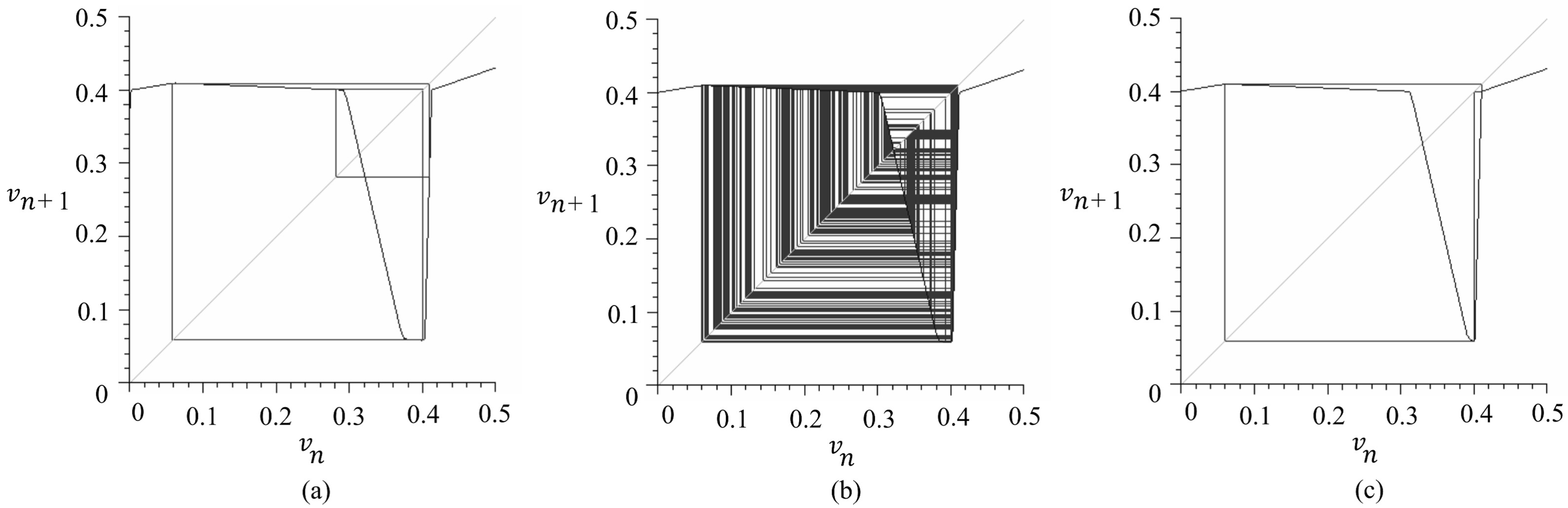
In the following, we show , , and and illustrate the v-i characteristic of and the graphs of and in Figure 8 and Figure 9, respectively. Further graphical iterative paths of and voltage map by Corollary 2 and iterative time series data of the voltage map at iterative time n are illustrated in Figure 10, Figure 11 and Figure 12, respectively. The conditions of these graphical iterations are as follows: the initial point of these iterations is , and with the use of Maple 8, the graphical iterations in these figures are illustrated by 2000 iterations such that the iterations from first until 1000 are not used in the total 3000 iterations. In addition, the real parameters of the conditions above are reasonable because [V], [V], , , , if , [V], and . The real transmission line circuit with three-segment piecewise linear resistor can be implemented.
5.2. Several Examples of Bifurcation Behavior of 1-D Maps
In this subsection, by using , we present various bifurcation behavior (including the found formal chaos) of 1-D voltage maps of Equation (18) with maximal Lyapunov exponent. The degree of observability of chaotic states is given by Lyapunov exponent of Equation (28) for any initial point [14].
Here, codimension one bifurcation diagrams with one of the bifurcation parameters: ζ, η, ξ, or E, and representative iterative paths are summarized as follows. With one of the following bifurcation parameters from bifurcation parameter ζ until bifurcation parameter E, the codimension one bifurcation diagrams including the found formal chaos togethar with the Lyapunov exponents, are illustrated in Figure 13, Figure 14, Figure 15 and Figure 16, respectively ( [V], [A], ).
- (1) bifurcation parameter:
- , ,, , .
- (2) bifurcation parameter:
- , , , , .
- (3) bifurcation parameter:
- , , , , .
- (4) bifurcation parameter E:
- , , , , .
Representative iterative paths in bifurcation diagrams of Figure 13, Figure 14, Figure 15 and Figure 16 are illustrated in Figure 17, Figure 18, Figure 19 and Figure 20, respectively. Graphical iterations in these figures are illustrated by 60 iterations such that the iterations from first until 40 are not used in the total 100 iterations. Since the voltage maps are composite maps consisting of incident waves or reflected waves, etc., it takes too much computation time to obtain bifurcation diagrams with Lyapunov exponents in Figure 13, Figure 14, Figure 15 and Figure 16. Therefore, the number of iterations for the voltage maps is intentionally reduced.
6. Conclusions
- We have described an implicit 1-D map of the incident and reflected waves that is derived from a lossless transmission line circuit with a dc bias voltage source in series with a load resistor at one side terminal and with a three-segment piecewise linear resistor at another side terminal.
- We have provided Theorem 1 establishing a 1-D map such as an incident wave: a reflected wave: ; Corollary 1 establishing 1-D map such as an incident wave: a reflected wave: ; and Corollary 2 establishing 1-D map such as a voltage: a voltage: in the case of Nagumo’s 3SPWL resistor or TD 3SPWL Resistor at the side terminal: .
- We have provided Theorem 3 such as an easy-to-use sufficient condition implying formal chaos existence in Definition 1.
- We have provided Theorem 2 to guarantee that for any initial point, every orbit by the iteration of the 1-D map ultimately penetrates in an invariant interval.
- We have provided Theorems 2 and 5 to guarantee that the dynamics of the second iterate map of the 1-D map on an invariant subset of the invariant interval has formal chaos.
- We have found that formal chaos exists under the condition such that [V], , , , , , , and .
- We have obtained the codimension of one type of four various bifurcation diagrams including the found formal chaos, with one of the bifurcation parameters: ζ, η, ξ, or E. From each bifurcation diagram with the Lyapunov exponent, the obsavability of the found formal chaos is considered to be rather high.
- As with the case of [12] such that the hidden dynamics of the circuit based on the integrated device has been unveiled on the basis of an analogy with the well-known Colpitts oscillator with the chaotic oscillations, we think that the hidden dynamics of imperfect transmission lines with parasitic effects and nonidealities inside real integrated devices can be unveiled on the basis of an analogy with the transmission line circuit of Equations (2)–(6) with formal chaos and that the parameters of the hidden dynamics can also be estimated by synchronizing a transmission line circuit with the chaotic oscillations acquired from the experimental circuit.
- We will report bifurcation processes with each of bifurcation parameters, Z or R, because nonlinear phenomena such as intermittency of chaos or blue sky bifurcation are observed in simulations.
- We will establish a method to find the bifurcation parameter ranges such that formal chaos exists for applications relative to several digital communication systems.
Author Contributions
H.O. supervised this research. H.N. and H.O. initiated the research, and contributed of a lossless transmission line circuit conceptualization and investigation of the transmission line circuit. K.O. and H.O. managed all of the research. H.O. provided theorems, and proofs. H.O. and K.O. contributed development of MAPLE simulation algorithm. K.O. also carried out the simulations. K.I. contributed validation of the methodology. K.O., K.I. and H.O. contributed the all of analysis result. The original manuscript was written by K.O., K.I. and H.O. And all of authors reviewed and edited the manuscript. All authors have read and agreed to the published version of the manuscript.
Funding
This research was supported by the research budget of the Graduate School of Electrical and Computer Engineering, Shonan Institute of Technology.
Institutional Review Board Statement
Not Applicable.
Informed Consent Statement
Not Applicable.
Data Availability Statement
Data is contained within the article.
Conflicts of Interest
The authors declare no conflict of interest.
Appendix A. Proofs of Theorems and Corollaries
Proof of Theorem 1.
Each of the proof for the case , or T, is given as follows.
- 1.
- In the case of : By using Equations (5) and (8), the break points and are transformed into and , respectively, such that the following is the case.and hold because and , respectively. Since -coordinate system is identical with the rotation of -coordinate system and and , as shown in Figure A1, is explicitly described by a three-segment piecewise linear function of Equation (16). , , , and hold because of the conditions such that and . Therefore, , , and hold.
- 2.
- In the case of : By using Equations (6) and (8), the break points and are transformed into and , respectively, such that the following is the case:and hold because and , respectively. Since the -coordinate system is identical with the rotation of -coordinate system and and , as shown in Figure A2, is explicitly described by a three-segment piecewise linear function of Equation (16). , , , , , and hold because of the conditions such that and . Therefore, , , and hold.
Figure A1.
The characteristics of Nagumo’s 3SPWL Resistor in and coordinate systems.
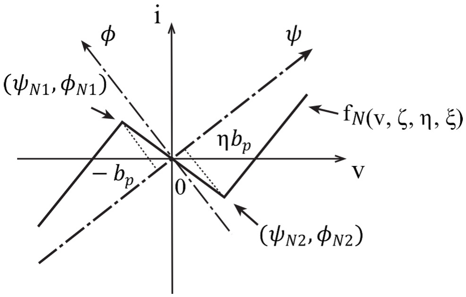
Figure A2.
The characteristics of TD 3SPWL Resistor in and coordinate systems.

The proof is now complete. □
Proof of Corollary 1.
Proof of Corollary 2.
Proof of Theorem 2.
Under the conditions that Theorem 2 holds, the following is the case.
In the case of : It is easy to check the following properties: (1) holds because and . (2) and , i.e., hold in the case of and .
Therefore, in the case of and , obviously holds because . Furthermore, for all x such as , holds because and for all x such as . = holds in the case of .
Therefore, for all x such as , the following is the case.
In a similar manner as the above, for all x such as , holds because and for all x such as .
= holds in the case of .
Therefore, for all x such as , the following is the case.
It is easy to check that and . Thus the 1-D map: has a unique unstable fixed point in the interval .
In the case of : It is easy to check the following properties: (1) holds because and . (2) and , i.e., hold in the case of and .
Furthermore, for all x such as , holds because and for all x such as . holds in the case of .
Therefore, for all x such as , the following is the case.
In the similar way above, for all x such as , holds because and for all x such as . holds in the case of .
Therefore, for all x such as , the following is the case.
It is easy to check that and . Thus, the 1-D map has a unique unstable fixed point in the interval .
Item 1 is proved.
Next, under the conditions that Theorem 2 holds, the following is the case.
In the case of , it is easy to check the following properties.
(1) , , and hold from Corollary 1. (2) because holds in the case of . (3) because holds in the case of .
In the case of , it is easy to check the following properties: (1) , , and hold from Corollary 1. (2) because holds in the case of . (3) because holds in the case of .
Therefore, there exists interval = such that . Furthermore, in the interval , has a positive slope such as . In the interval , has negative slope such as . In the interval , has positive slope such as .
Then, holds because holds. In the similar way above, holds because holds. Therefore, it is confirmed that and . Thus holds.
Item 2 is proved.
Finally for any , clearly . for any , from Equation (A1) or Equation (A3). is a monotonically increasing sequence. Therefore, for any , there exists jth iterate of such that . In the similar way for any , from Equation (A2) or Equation (A4). is a monotonically decreasing sequence. Therefore, for any , there exists jth iterate of such that . Item 3 is proved. The proof is now complete. □
Proof of Theorem 3.
Definition A1
(Devaney [15])
or .
is called the sequence space on the two symbols 0 and 1. Elements of are infinite sequences of integers, such as or . We may make into a metric space as follows. For two sequences and , define the distance between them by . Since is either 0 or 1, this infinite series is dominated by the geometric series ; therefore, it converges.
Definition A2
(Devaney [15]). The shift map is given by .
The shift map simply “forgets” the first entry in a sequence, and shifts all other entries one place to the left. Clearly, σ is a two-to-one map of , as may be either 0 or 1. Moreover, in the metric defined above, σ is a continuous map.
Proposition A1
(Devaney [15]). is a metric on .
Proposition A2
(Devaney [15]). Let and suppose for . Then, . Conversely, if , then for .
Proposition A3
(Devaney [15]). is continuous.
Definition A3
(Devaney [15]). The itinerary of x is a sequence where if , , if,.
Thus, the itinerary of x is an infinite sequence of 0s and 1s. That is, is a point in the sequence space . We think of S as a map from Λ to . This map has several interesting properties.
Let or be a closed interval. Let . . Since item above holds, exists as the preimage of J under functions .
Let
.
consists of two closed subintervals, one in and one in . Hence, consists of four disjoint closed subintervals, two in and two in . Similarly, in general, consists of closed subintervals, in and in . Hence, consists of disjoint closed subintervals, in and in . Then, the sequence is not empty. We have . First, we consider the properties of the sequence . Note that and hold. We may assume that is a nonempty subinterval so that, by the observation above, consists of two closed intervals, one in and one in . Hence, is a single closed interval. forms a nested sequence of nonempty closed intervals because .
Therefore, we conclude that is nonempty closed, set and Λ is also nonempty closed set such that .
Secondly, we show that S is one to one. Let and suppose . Then, for each n, and lie on the same interval or . This implies that f is monotone on the interval between and . Consequently, all points in this interval remain in when we apply f. Now, at all points in this interval; thus, as in item , each iteration of f expands this interval by a factor of K. Hence, the distance between and grows without bound, so these two points and must eventually lie on and (or and ), respectively. This contradicts the fact that they have the same itinerary.
Thirdly, to see that S is onto, let . We must produce with . Note that if , then , etc. Hence, there exists such that . This proves that S is onto. Observe that consists of a unique point because S is one to one. In particular, we have that diameter of tending to 0 as .
Furthermore, to prove the continuity of S, we choose and suppose that . Let . Pick n so that . Consider the closed subintervals defined above for all possible combinations . These subintervals are all disjoint, and Λ is contained in their union. These are such intervals, and is one of them. Hence, we may choose δ such that and implies that . Therefore, agrees with in the first terms. Thus, by Proposition A2, we have . This proves the continuity of S. Since Λ is compact (bounded closed sets) and S is continuous and one to one, is also continuous. Thus, S is a homeomorphism.
Finally, to prove that , i.e., S provides an equivalence between the dynamics of f on Λ and σ on . Let and suppose that . Then, we have and so forth. However, the fact that , etc., says that , so , which is what we wanted to prove. The proof is now complete. □
Proof of Theorem 4.
Let be the set of real numbers. Under the conditions that Theorem 4 holds, it is easy to check the following properties: (1) the break points and are given by the solutions of and , respectively. (2) The break points of : and are also the break points of . (3)The break points and are given by the solutions of and , respectively. (4) holds because , and hold. (5) The break points and are given by the solutions of and , respectively. (6) holds because and hold.
Furthermore, because and . because , , and . because and . because and . because , and . because and . The proof is now complete. □
Proof of Theorem 5.
Under the conditions of Theorem 5, Theorem 4 holds. In the following, is given by the map of Theorem 4. Then , , and . Therefore, clearly . also holds for because . , , and . Therefore, holds because holds. also holds for because . Thus, item 1 is proved.
Next to prove the item 2, it is sufficient that is considered as the map f in Theorem 3. Under the item 1 condition, is satisfied with the condition of Theorem 3. The item 2 is also proved. The proof is now complete. □
References
- Saito, T. A Chaos Generator Based on a Quasi-Harmonic Oscillator. IEEE Trans. Circuits Syst. 1985, 32, 320–331. [Google Scholar] [CrossRef]
- Saito, T.; Nakagawa, S. Chaos from a hysteresis and switched circuit. Philos. Trans. R. Soc. Lond. Math Phys. Sci. 1995, 352, 47–57. [Google Scholar]
- Miyoshi, T.; Saito, T.; Inaba, N. Chaotic Phenomena in a Iron Resonant Circuit Including an Inductor with Complete Saturation Characteristic. IEICE Trans. 1997, 80, 346–354. (In Japanese) [Google Scholar]
- Kennedy, M.P.; Rovatti, R.; Setti, G. (Eds.) Chaotic Electronics in Telecommunications; CRC Press: Boca Raton, FL, USA, 2000. [Google Scholar]
- Nagumo, J.; Shimura, M. Self-oscillation in a transmission line with a tunnel diode. Proc. IRE. 1961, 49, 1281–1291. [Google Scholar] [CrossRef]
- Nagumo, J.; Sato, S. On a Response Characteristic of a Mathematical Neuron Model. Kybernetik 1972, 10, 155–164. (In Japanese) [Google Scholar] [CrossRef] [PubMed]
- Nakano, H.; Okazaki, H. Bifurcation Phenomena of a Distributed parameter System with a Nonlinear Element Having Negative Resistance. IEICE Trans. Fundam. 1992, 75, 339–346. [Google Scholar]
- Sharkovsky, A.N.; Maistrenko, Y.U.; Deregel, P.H.; Chua, L.O. Dry Turbulence a Time-Delayed Chua’s Circuit. J. Circuits Syst. Comput. 1993, 3, 645–668. [Google Scholar] [CrossRef]
- Sharkovsky, A.N. Chaos from a Time-Delayed Chua’s Circuit. IEEE Trans. Circuits Syst. 1993, 40, 781–783. [Google Scholar] [CrossRef]
- Sharkovsky, A.N.; Romanenko, E.; Berezovsky, S. Ideal turbulence: Definition and models. In Proceedings of the 2003 IEEE International Workshop on Workload Characterization (IEEE Cat. No.03EX775), St. Petersburg, Russia, 20–22 August 2003; Volume 1, pp. 23–30. [Google Scholar]
- Miyabayashi, N.; Moro, S.; Mori, S. Spatio-temporal dynamics in an array of time delayed Van der Pol oscillators. In Proceedings of the 1997 IEEE International Symposium on Circuits and Systems (ISCAS ’97), Hong Kong, China, 12 June 1997; Volume 2, pp. 917–920. [Google Scholar]
- Bucolo, M.; Buscarino, A.; Famoso, C.; Fortuna, L.; Gagliano, S. Imperfections in Integrated Devices Allow the Emergence of Unexpected Strange Attractors in Electronic Circuits. IEEE Access 2021, 9, 29573–29583. [Google Scholar] [CrossRef]
- Kohda, T. Discrete Dynamics and Chaos; Corona Publishing: Tokyo, Japan, 1998. (In Japanese) [Google Scholar]
- Guckenheimer, J.; Holmes, P. Nonlinear Oscillations Dynamical Systems, and Bifurcation of Vector Fields; Springer: New York, NY, USA, 1983. [Google Scholar]
- Devaney, R.L. An Introduction to Chaotic Dynamical Systems; The Benjamin/Cummings Publishing: San Francisco, CA, USA, 1986. [Google Scholar]
- Robinson, C. Dynamical Systems, Stability, Symbolic Dynamics, and Chaos, 2nd ed.; CRC Press: Boca Raton, FL, USA, 1999. [Google Scholar]
- Kokubu, H. Foundation of Dynamical Systems; Asakura Publishing: Tokyo, Japan, 2000. (In Japanese) [Google Scholar]
- Thunberg, H. Periodicity versus Chaos in One-Dimensional Dynamics. SIAM Rev. 2001, 43, 3–30. [Google Scholar] [CrossRef] [Green Version]
- Moser, J. Stable and Random Motions in Dynamical Systems; Princeton University Press: Princeton, NJ, USA, 1973. [Google Scholar]
- Oono, Y.; Oshikawa, M. Chaos in Nonlinear Difference Equations I. Prog. Theor. Phys. 1980, 64, 54–67. [Google Scholar] [CrossRef] [Green Version]
- Aoki, N. Dynamical Systems and Chaos-Geometric Construction of Nonlinear Phenomena; Kyoritsu Publishing: Tokyo, Japan, 2000. (In Japanese) [Google Scholar]
- Okazaki, H.; Okazaki, C.; Honda, H.; Nakano, H. Rigorous verification of formal chaos produced by one-dimensional discrete dynamical system with use of interval arithmetic. In Proceedings of the 2005 IEEE 48th Midwest Symposium on Circuits and Systems (The IEEE MWSCAS 2005), Covington, KY, USA, 7–10 August 2005; pp. 1597–1660. [Google Scholar]
- Lynch, S. Dynamical Systems with Applications Using MAPLE; Birkhäuser: Basel, Switzerland, 2010. [Google Scholar]
Figure 1.
Op amp circuit based Nagumo’s 3SPWL resistor.
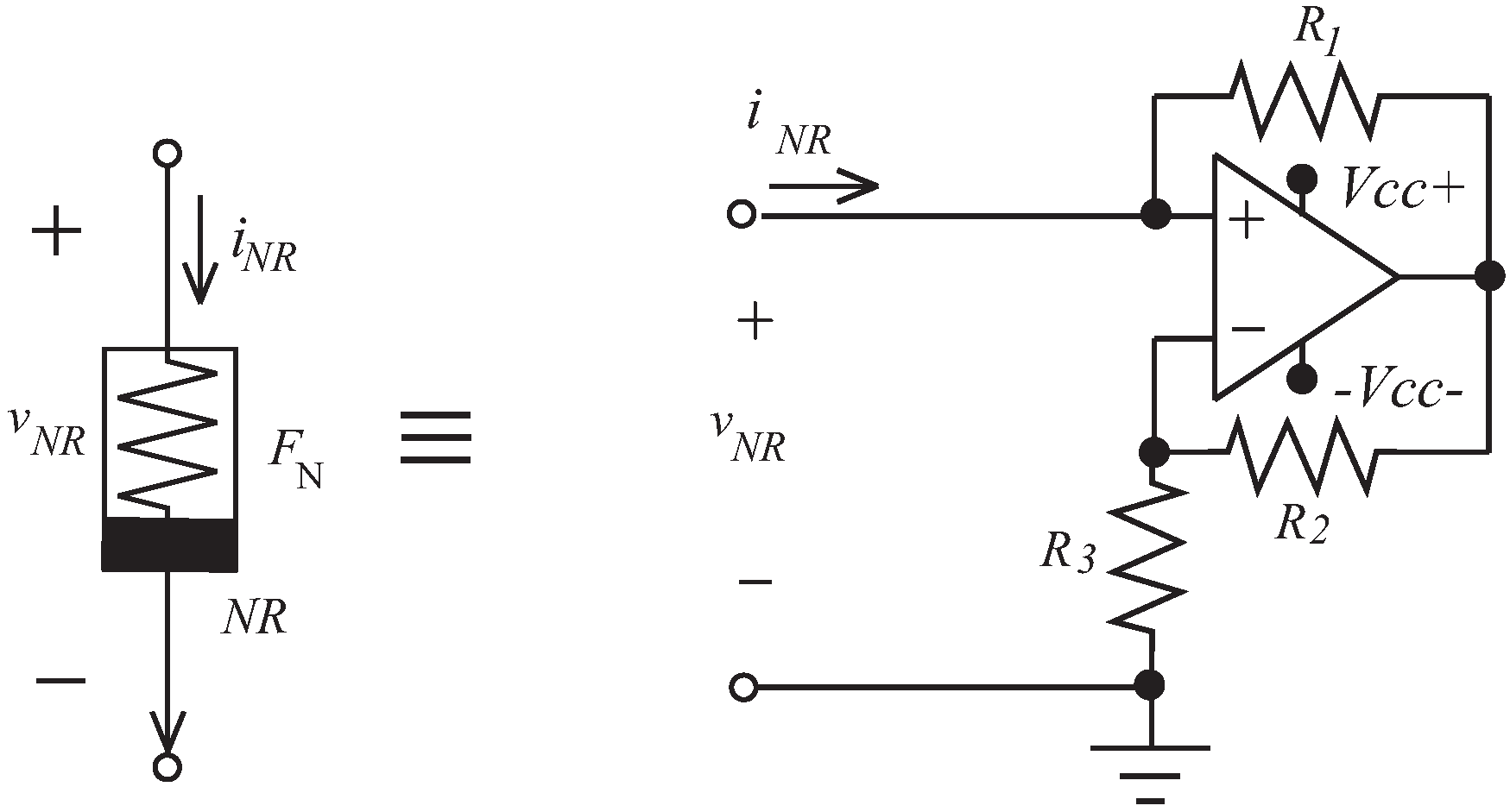
Figure 2.
− characteristic of Nagumo’s 3SPWL resistor.

Figure 3.
Op amp circuit based Modeled Tunnnel Diode 3SPWL resistor.
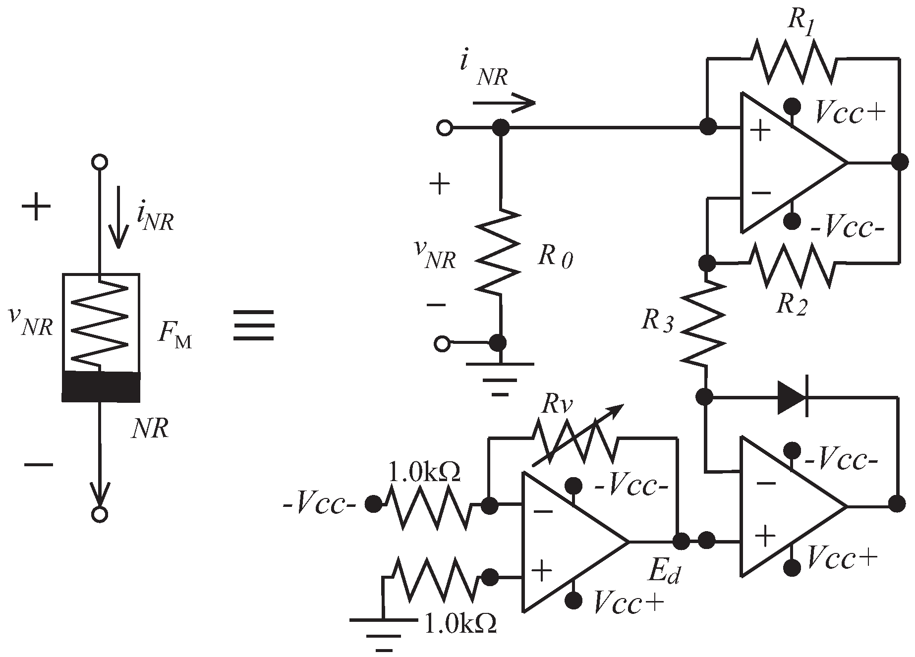
Figure 4.
− characteristic of Modeled Tunnnel Diode 3SPWL resistor.
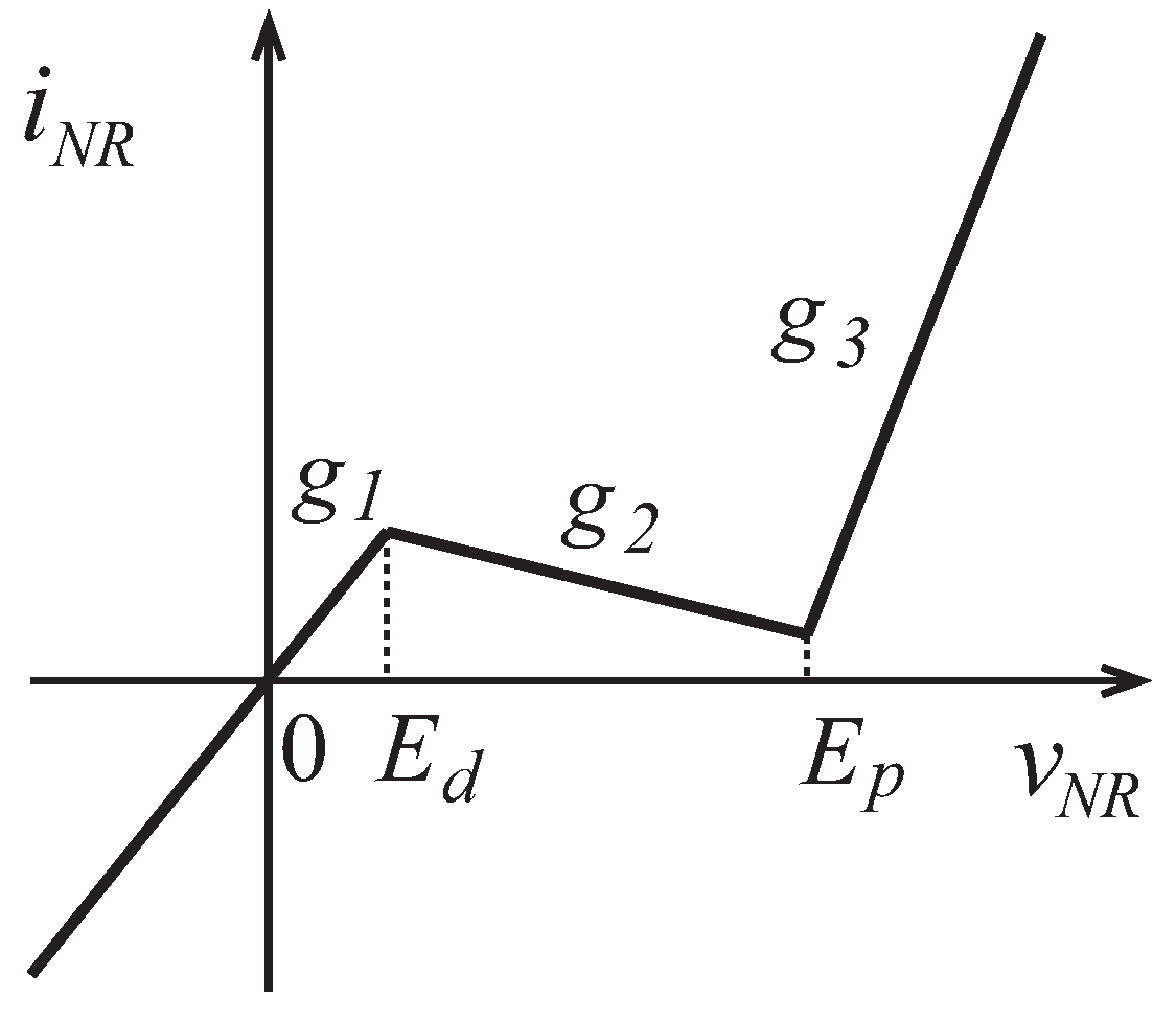
Figure 5.
Transmission line circuit with generally practical side terminal conditions.
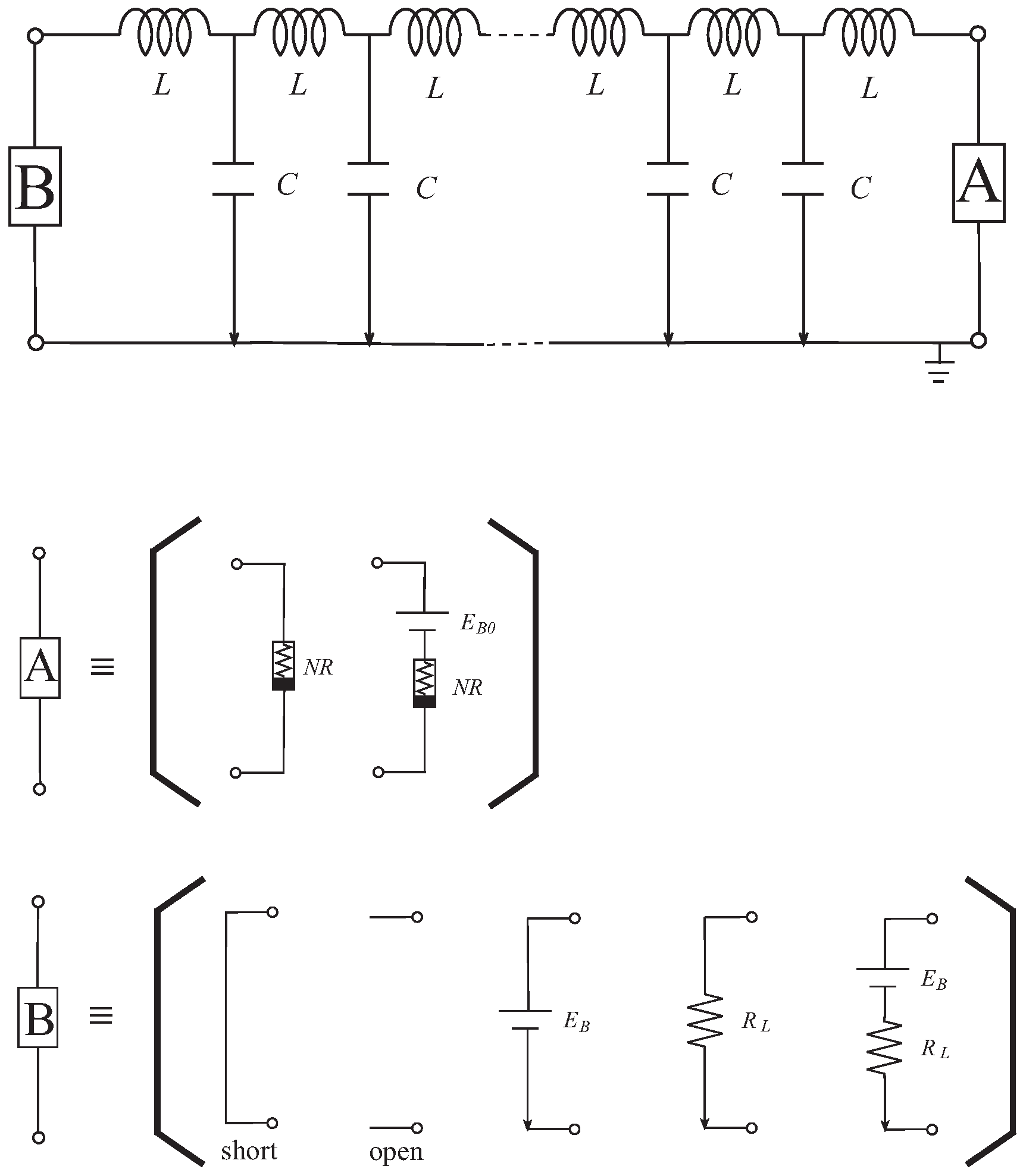
Figure 6.
Transmission line circuit with standard side terminal conditions.
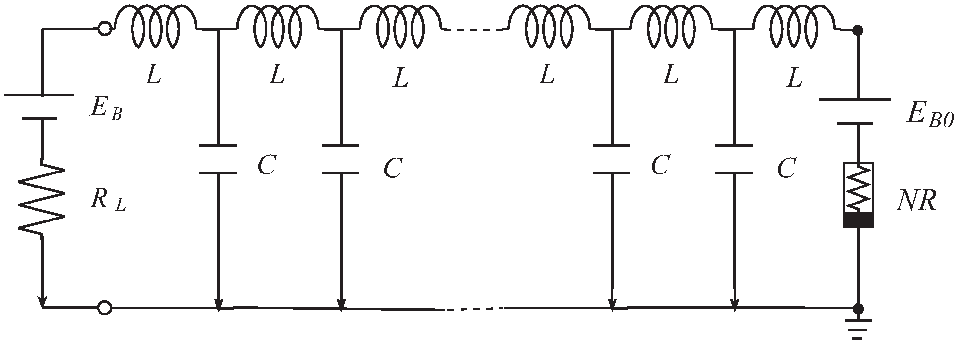
Figure 7.
Normalized 1-D map.
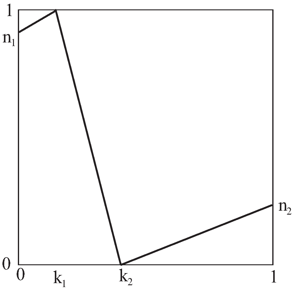
Figure 8.
v-i characteristic of .
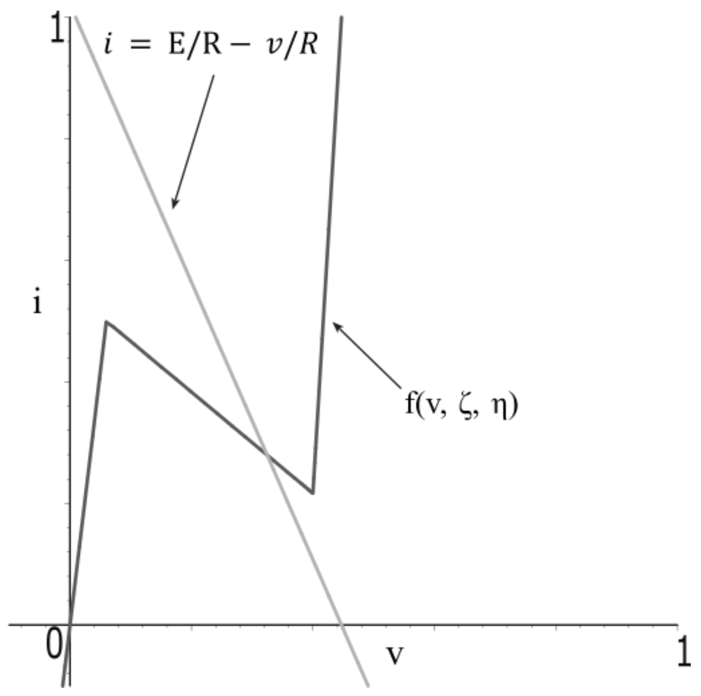
Figure 9.
and .
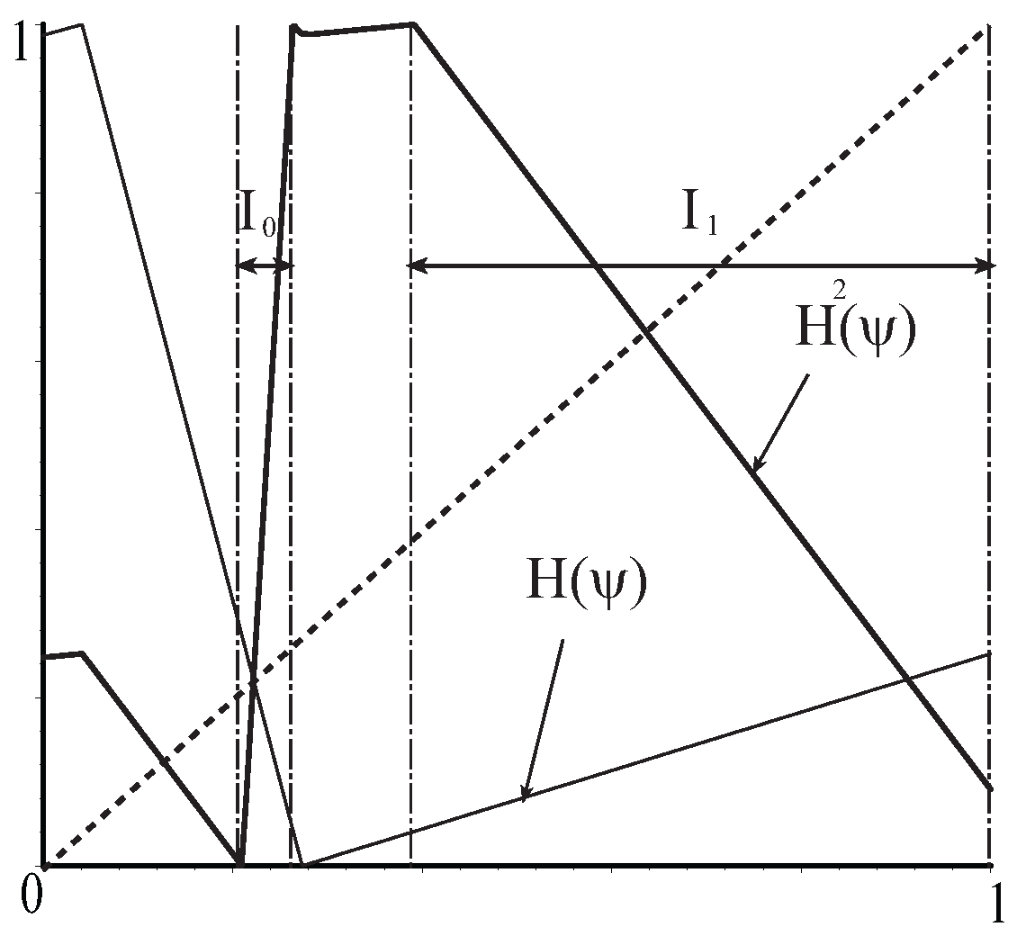
Figure 10.
Iterative paths of .
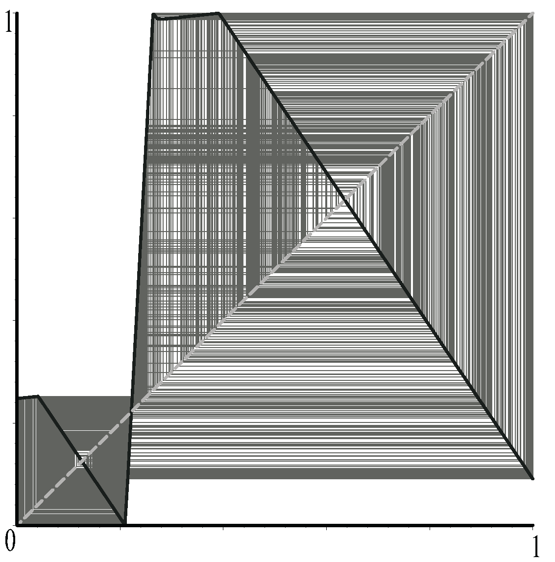
Figure 11.
Iterative paths of voltage map.

Figure 12.
Time series data of voltage map at iterative time n.
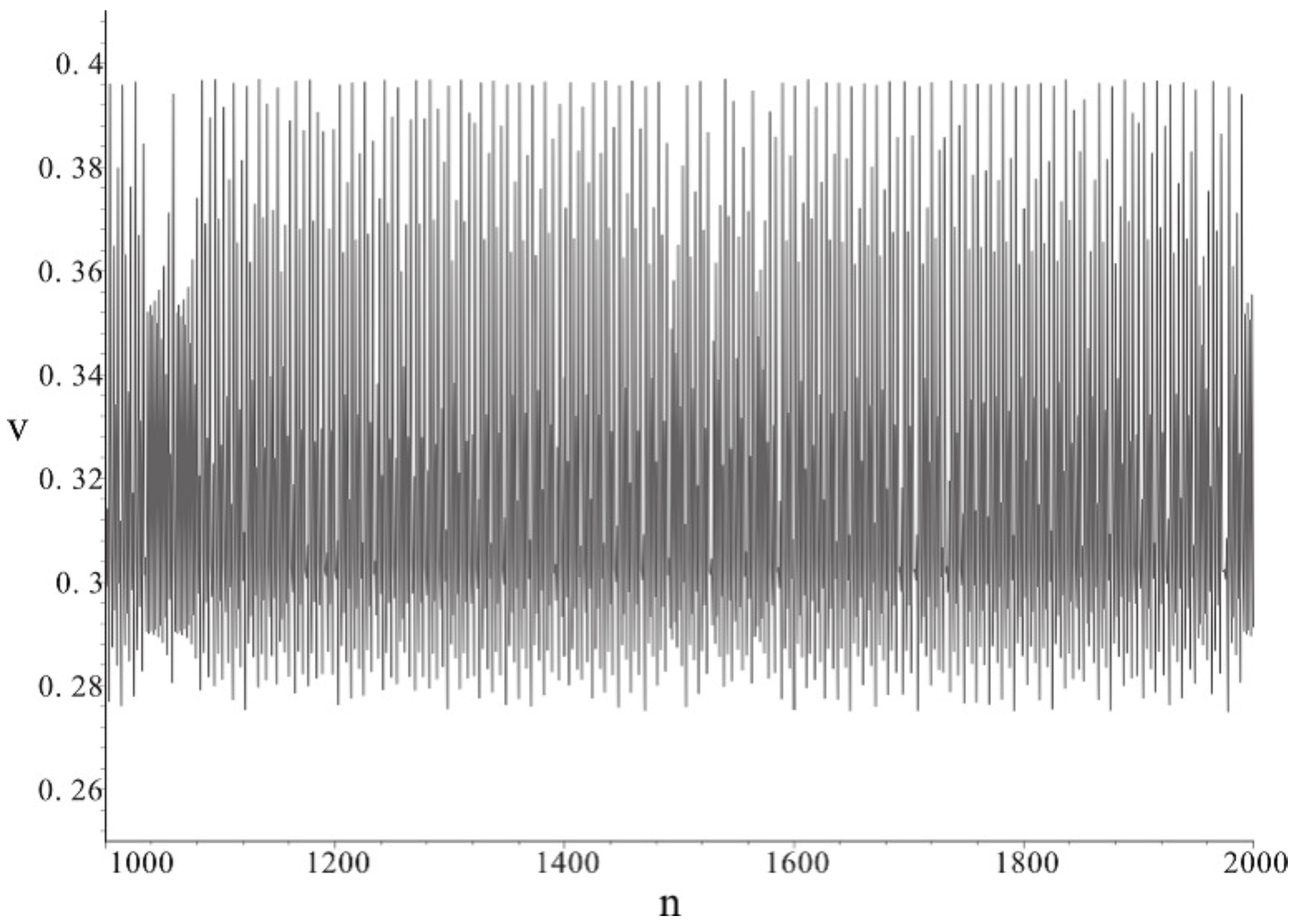
Figure 13.
Bifurcation diagram with ζ parameter.
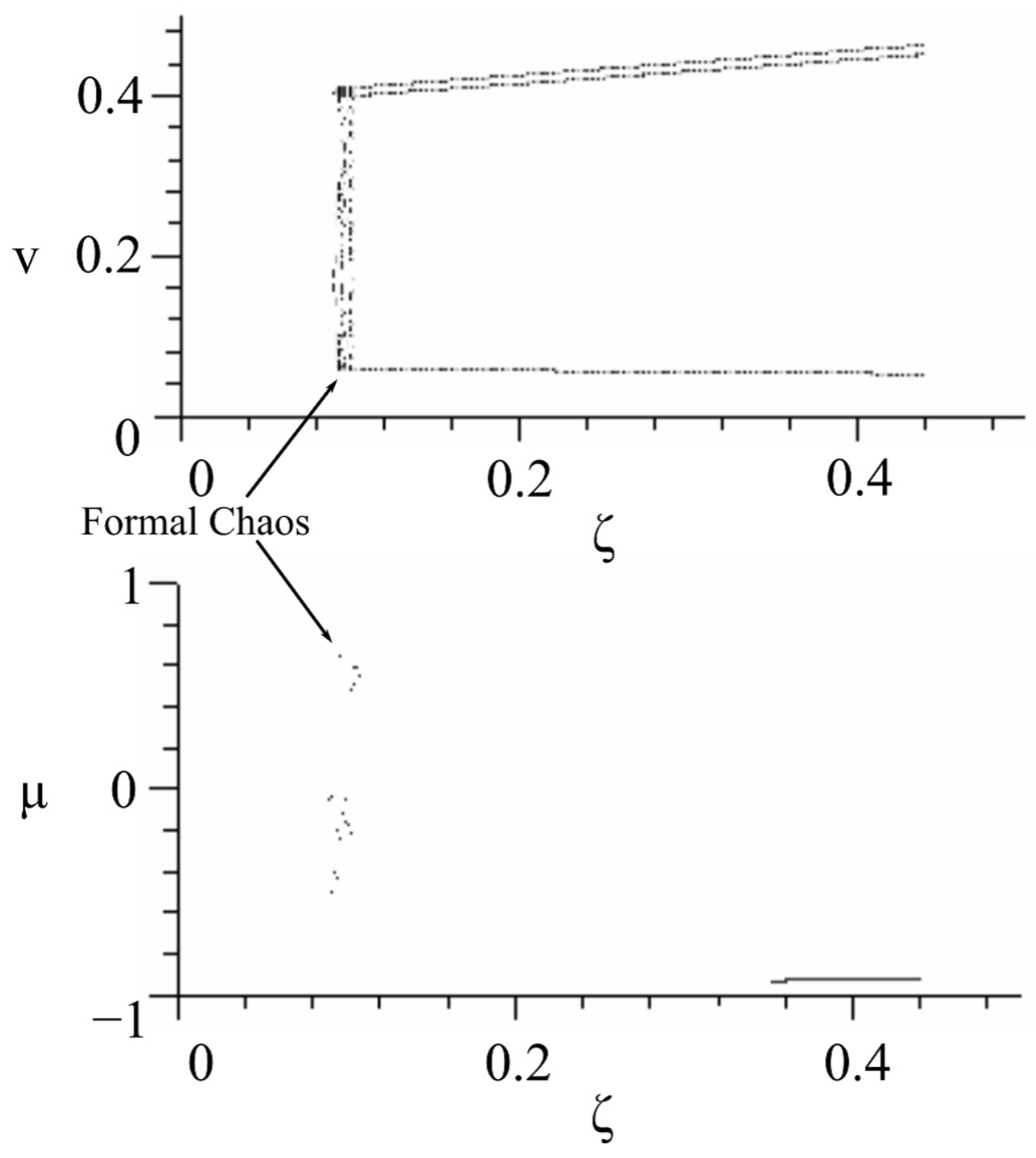
Figure 14.
Bifurcation diagram with η parameter.
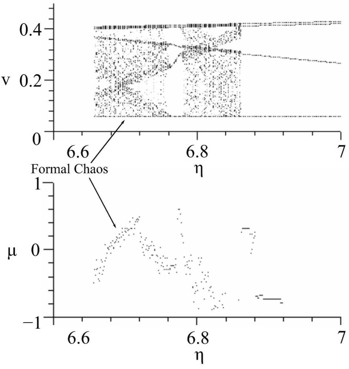
Figure 15.
Bifurcation diagram with ξ parameter.

Figure 16.
Bifurcation diagram with E parameter.
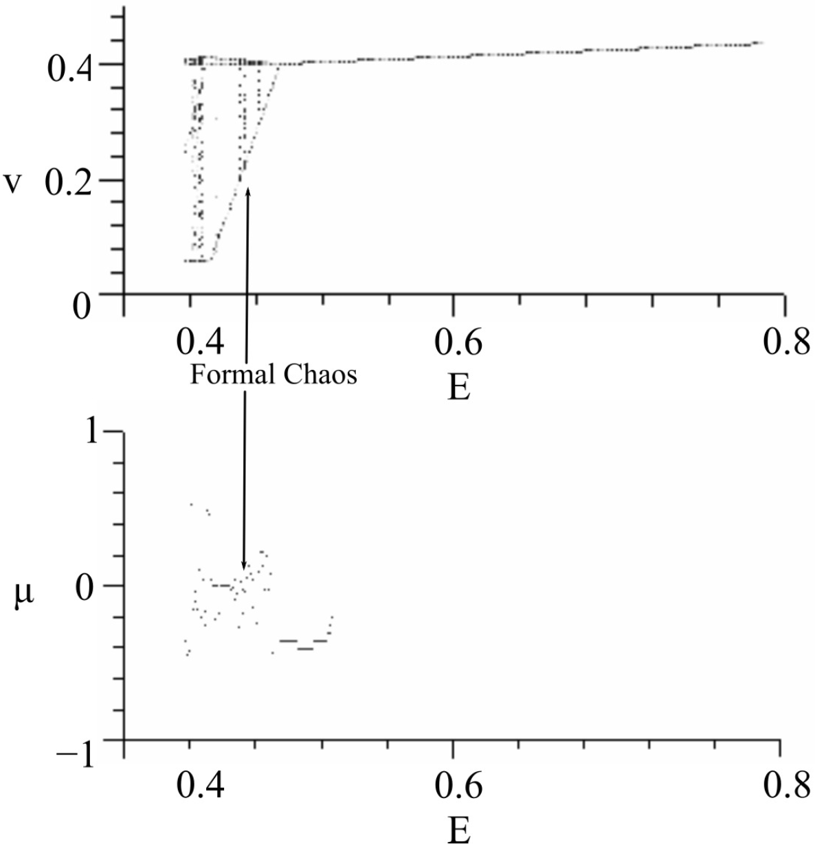
Figure 17.
Iterative paths with the initial point: . (a) . (b) . (c) .
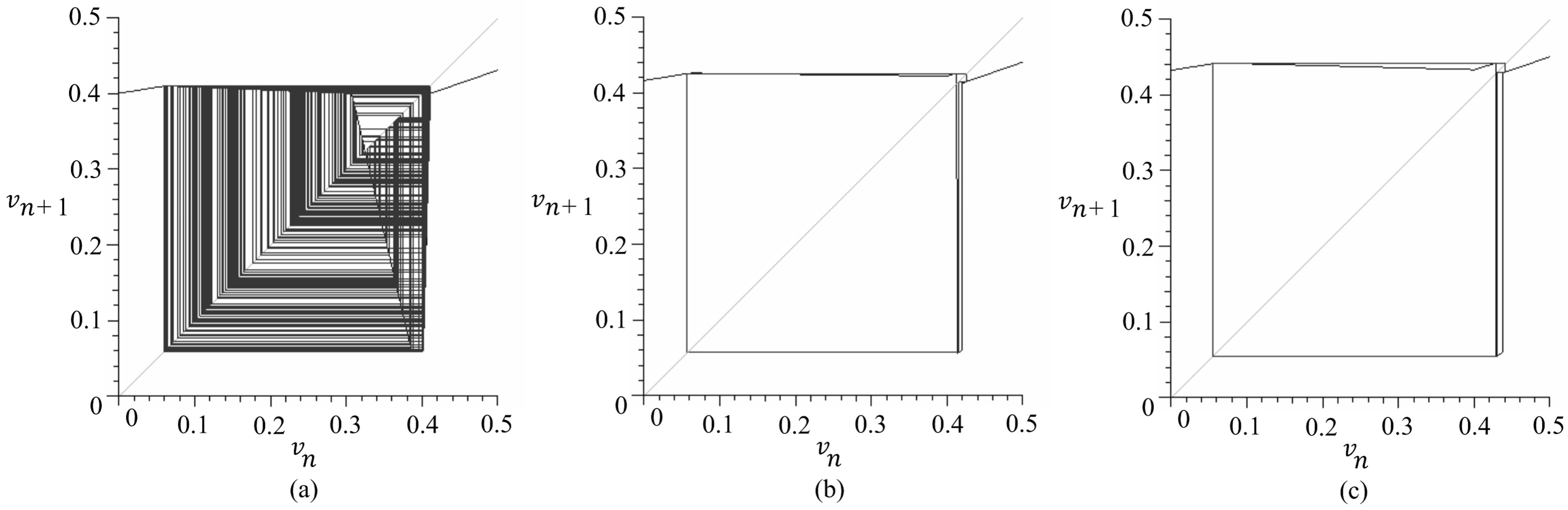
Figure 18.
Iterative paths with the initial point: . (a) . (b) . (c) .
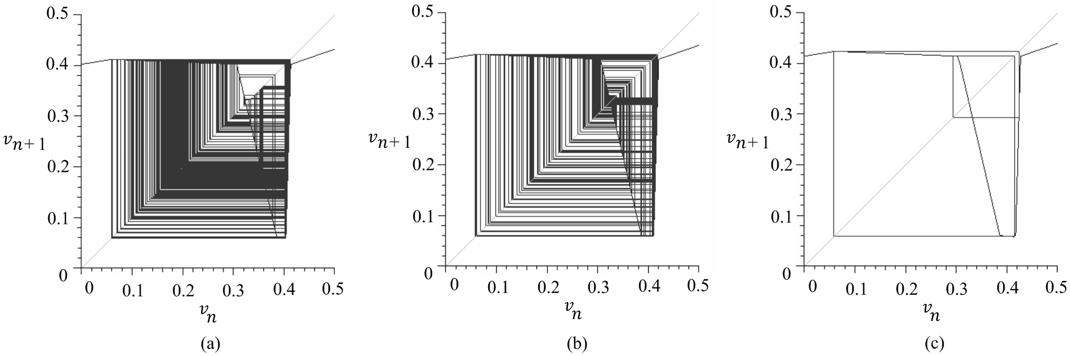
Figure 19.
Iterative paths with the initial point: . (a) . (b) . (c) .
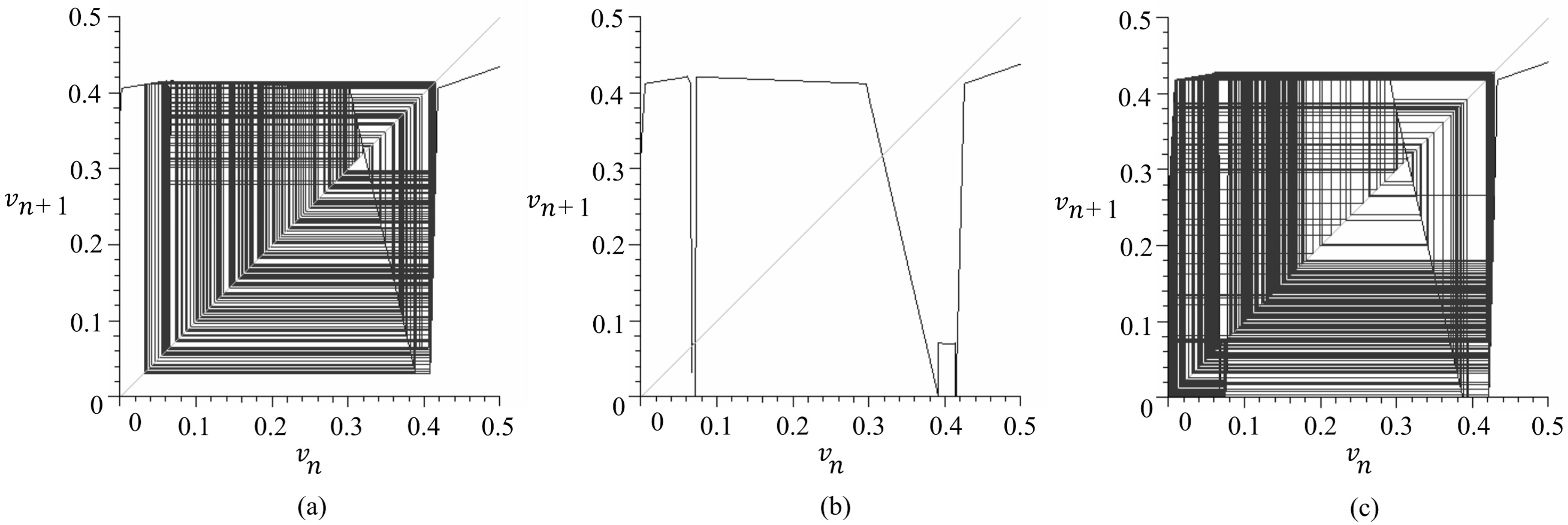
Figure 20.
Iterative paths with the initial point: . (a) . (b) . (c) .
Publisher’s Note: MDPI stays neutral with regard to jurisdictional claims in published maps and institutional affiliations. |
© 2021 by the authors. Licensee MDPI, Basel, Switzerland. This article is an open access article distributed under the terms and conditions of the Creative Commons Attribution (CC BY) license (https://creativecommons.org/licenses/by/4.0/).
Share and Cite
MDPI and ACS Style
Ozawa, K.; Isogai, K.; Nakano, H.; Okazaki, H. Formal Chaos Existing Conditions on a Transmission Line Circuit with a Piecewise Linear Resistor. Appl. Sci. 2021, 11, 9672. https://doi.org/10.3390/app11209672
AMA Style
Ozawa K, Isogai K, Nakano H, Okazaki H. Formal Chaos Existing Conditions on a Transmission Line Circuit with a Piecewise Linear Resistor. Applied Sciences. 2021; 11(20):9672. https://doi.org/10.3390/app11209672
Chicago/Turabian StyleOzawa, Kazuya, Kaito Isogai, Hideo Nakano, and Hideaki Okazaki. 2021. "Formal Chaos Existing Conditions on a Transmission Line Circuit with a Piecewise Linear Resistor" Applied Sciences 11, no. 20: 9672. https://doi.org/10.3390/app11209672
Note that from the first issue of 2016, this journal uses article numbers instead of page numbers. See further details here.