
Compact Beam Homogenizer Module with Laser-Fabricated Lens-Arrays

1
Applied Laser and Photonics Group, University of Applied Sciences Aschaffenburg, Würzburger Straße 45, 63743 Aschaffenburg, Germany
2
Applied Laser Technologies, Ruhr University Bochum, Universitätsstraße 150, 44801 Bochum, Germany
*
Author to whom correspondence should be addressed.
Appl. Sci. 2021, 11(3), 1018; https://doi.org/10.3390/app11031018
Submission received: 8 December 2020
/
Revised: 20 January 2021
/
Accepted: 21 January 2021
/
Published: 23 January 2021
(This article belongs to the Special Issue Advanced Laser Beam Shaping for Micro Material Processing)
Abstract
:We report on manufacturing of a compact beam homogenizer module including two lens arrays and an aperture. Lens arrays are fabricated by an all laser-based technology employing a precise femtosecond pulsed laser ablation and a CO laser polishing step. Each lens array is processed revealing a high contour accuracy and a roughness of 25 nm. The 8x8 lens arrays are designed to have a square footprint to generate a quadratic Top-Hat beam profile and focal length of 10 mm to realize compact packaging. Firstly, the lens arrays are tested in an experimental setup using commercial lens holders with their functionality being demonstrated by shaping a uniform 4.5 mm squared Top-Hat beam profile, as being calculated. Afterwards, a 3D printer is used to additively manufacture the housing for the beam homogenizer module having a length of only 16 mm. After assembling the laser-fabricated lens arrays and a laser-cutted aperture into the housing, the functionality of the miniaturized module is proven.
1. Introduction
Lens arrays have been demonstrated to be applied in numerous fields of optics such as, e.g., in sensor applications as in Shack-Hartman sensors for wave front detection [1], in imaging systems as for microscopy [2] or photolithography [3] or for increasing the light extraction efficiency in organic light-emitting diodes/devices [4,5]. Furthermore, lens arrays are used for beam homogenization to ensure uniform illumination as being employed in, e.g., beam-shaping of excimer laser beam profile [6], petawatt-class Ti:sapphire amplifier [7], planar laser diagnostics [8] or illumination systems [9]. Two types of lens array based beam homogenizers are discussed in literature, the non-imaging applying one lens array and a Fourier lens and the imaging beam homogenizer including two lens arrays and a Fourier lens [10]. Figure 1 shows an imaging beam homogenizer with two lens arrays LA1 and LA2 as well as a Fourier lens. The first lens array is used to split the incoming light into several beamlets which are located on the second lens array and further focused and overlapped by a Fourier lens, forming a homogeneous intensity profile. The contour of the final beam profile is given by the footprint of the single elements within the lens arrays. Using Equation (1) [6], the size of the corresponding Top-Hat profile in the focal plane of the Fourier lens can be calculated with p being the lens pitch, a the distance between the two lens arrays, F the focal length of the Fourier lens, as well as and the arrays’ focal lengths.
If the imaging condition () is fulfilled, the size of the Top-Hat can be calculated with the simplified Equation (2) while the distance b between the second lens array and the Fourier lens can be chosen freely due to not affecting the size of the formed Top-Hat (see Equation (2)) and will only influence its divergence [7,11].
While lens arrays are often fabricated via thermal reflow processes [22,23,24], several alternative methods such as ink-jetting [25], reactive ion etching [26] or hot embossing [27] have been demonstrated. Recently, femtosecond laser-based lens array fabrication techniques have been developed which are summarized in Table 1. Hua et al. [12] demonstrated the usage of the femtosecond laser in a backside wet etching process for geometry generation, which is followed by thermal annealing to smoothen the surface to fabricate microlens arrays in silica. Pan et al. [13] and Zhang et al. [14] showed the microlens array fabrication by femtosecond laser production of microholes and a subsequent wet etching step forming the lens geometry on silicon as well as silica and sapphire, respectively. Lin et al. [15] modified photosensitive glass with a femtosecond laser which is further processed via thermal treatment, wet etching and annealing to fabricate the finalized optic. Yong et al. [16] fabricated microlens arrays with femtosecond lasers, while a single pulse is sufficient to form a single lens in PDMS by the laser-induced plasma expansion and its mechanical pressure as well as a long resolidification time of the material. A similar process has been shown by Kardan et al. [17] to fabricate single shot lenses in chalcohalide glass. Also the two-photon polymerization process can be used to fabricate different types of polymeric lens arrays shown by Wu et al. [18] and He et al. [19]. Choi et al. [20] and Delgado et al. [21] applied the femtosecond laser to fabricate periodic microstructures in fused silica and soda lime glass, respectively, which are further polished and reshaped by a CO-laser step to polish the preform and form the desired geometry. A similar process applying both, a femtosecond and a CO-laser is also used in our lens array fabrication process. While a reshaping is essential in the previous publications, we define the lens geometry by precise layer-wise ablation with the femtosecond laser. In a second process, the CO laser is used to reduce the previously introduced surface roughness while a reshaping of the initially femtosecond laser-generated geometry is supposed to be minimized. Furthermore, the most standard lens array fabrication processes use polymer substrates or include an etching step, while our process offers the fabrication of glass lens arrays without using polymer substrates or etching.
2. Experimental
Lens arrays are fabricated out of fused silica within a two-step all laser-based manufacturing process shown in Figure 2. Firstly, a Yb:KGW femtosecond pulsed laser (Pharos, Light Conversion, Vilnius, Lithuania) having a wavelength of 1030 nm, a pulse duration of 230 fs (FWHM) and a repetition rate of 50 kHz is used to ablate the lens array preforms. The laser is equipped to a micromachining system (MM200-USP, Optec, Frameries, Belgium) including a galvanometer scanner (RTA AR800 2G+, Newson, Dendermonde, Belgium) with a telecentric f-Theta-lens having a focal length of 100 mm resulting in a focal diameter of 33 µm (1/e), measured with a high-resolution camera (UI-1490SE-M-GL, IDS, Obersulm, Germany). Due to its wide-ranging usage for optical components, polished fused silica (GVB GmbH, Herzogenrath, Germany) is applied in our experiments having a diameter of 14 mm and a thickness of 2 mm. The lens array geometries are created by a layer-wise removal of the silica substrate in steps of 1 µm in height for a high contour accuracy. Within each layer, contour adapted hatches consisting of parallel lines are scanned by the laser. Therefore, a pulse distance of 12 µm in both, scanning direction and perpendicular thereto is chosen resulting in a scanning speed of 600 mm/s and a line distance of 12 µm corresponding to a pulse overlap of 64%. A fluence of 2.37 J/cm is applied to precisely remove 1 µm substrate within each layer. After each layer, the focal position of the laser is adjusted by a motorized z-stage (PRO165, Aerotech, Pittsburgh, PA, USA) and the hatch orientation is rotated by 100 to avoid consecutive overlapping scanning paths for a homogeneous ablation process. Please note, the glass substrate was initially roughened with adapted laser parameters due to changes in morphology and absorption behaviour (compared to the polished substrate) which is necessary in order to achieve comparable absorption and ablation behaviour of each ablated layer. Secondly, a CO laser (Infinity, Iradion, Uxbridge, MA, USA) having a wavelength of 10.6 µm is used to polish the previously generated preform. The CO laser is scanned across the sample by a flying optic having a focal length of 63.5 mm. A defocus of 20 mm is applied resulting in a spot diameter on the sample surface of 1.5 mm (1/e). Hatches consisting of straight, parallel lines having a line distance of 25.4 µm are scanned twice. The geometry of the hatch is designed to be a circle with a diameter of 16 mm to scan over the entire samples (Ø = 14 mm) for a complete heating of the glass substrate. Both scans are executed with a laser power of 73 W at the sample surface allowing a high scanning speed. The first pass is used to polish the sample, while the second pass removes smaller debris remaining at the surface. For both passes, different scanning speeds are chosen, 142 mm/s for the first and 178 mm/s for the second pass, respectively. A similar process chain for the manufacturing of optical elements such as cylindrical lenses [28], convex and concave axicons [29,30] as well as axicon arrays [31] has been demonstrated previously. To analyze the generated 3D structures in detail, a laser scanning microscope (LSM, VK-X210, Keyence, Osaka, Japan) is used.
3. Results and Discussion
Figure 3a shows a LSM image of the final fused silica lens array consisting of 64 lenses. The lenses are designed to have a radius of 4.5 mm resulting in a focal length of 10 mm, calculated by f = R/(n−1), with R being the lens radius and n = 1.45 the refractive index of fused silica at 1030 nm [32]. Furthermore, the individual lenses reveal a square footprint for both, resulting in a fill factor of 100% and required to generate square shaped Top-Hat beam profiles when used in a beam homogenizer setup. The edge length of the individual lenses is designed to be 1 mm. Apparently, the lens array consists of uniform lenses, while the magnification exemplarily shows the contour of a single lens. Here, the roughness R is 25 nm, measured along lines within an area of 900 µm × 900 µm (to exclude the corner points). The corresponding cross-section (blue line) also demonstrates the smooth surface contour of the lens, while a circle fit (red area) revealing a radius of 4.5 mm is added to show comparison with the ideal radius. Apparently, the fabricated lens is in excellent agreement with the designed curvature. Smaller roundings are found at the intersection points of two adjacent lenses, which are caused by the melted glass within the polishing process. However, the lens arrays are fabricated with high contour accuracy and a high degree of uniformity overall. Before applying the lens arrays in a beam homogenizer setup, the fabricated optics are tested in a simple setup consisting of a screen, showing the letter “A”, the fabricated lens array and a USB microscope (VMS-004 Deluxe, Veho, Southampton, England) shown in Figure 3b. The captured image clearly shows multiple letters “A”, demonstrating the proper imaging quality and thus the functionality of the tested lens array.
To demonstrate the beam homogenizing properties in detail, an optical setup as shown in Figure 4 is used in our experiments. The setup includes a halogen light source (LS 100-130, Instrument Systems, Munich, Germany), a plano-convex collimator lens (CL), an iris diaphragm, the laser-fabricated lens arrays, a Fourier lens (FL) and a CMOS camera (LaserCam-HR, Coherent, Santa Clara, CA, USA).
Figure 5a shows the beam profile taken behind the iris diaphragm. Obviously, the halogen light source reveals inhomogeneous intensity distribution, which is clearly visible in the cross-sections. Figure 5b shows the beam profile taken after beam homogenisation. Apparently, a flat Top-Hat profile is formed, demonstrating the functionality of our lens arrays. The flat Top-Hat is also visible in the cross-sections in both, x- and y-direction, with a marker showing the Top-Hat size of 4.5 mm at full width half maximum. By using two lens arrays with equal focal lengths (10 mm), the theoretical size of the Top-Hat can be calculated by the simplified Equation (2). With the lens pitch being 1 mm, the focal length of the Fourier lens being 50 mm and the distance between the two lens arrays being 11 mm, the Top-Hat is calculated to have a size of 4.5 mm. Based on Equation (2), the Top-Hat size can be easily altered by changing the focal length of the Fourier lens.
Obviously, the generated Top-Hat is in excellent agreement with theoretical assumptions. To characterize the generated profile in more detail, the applied laser camera offers calculations of the most important parameters according to ISO 13694:2000(E) for a threshold of 90%, important for the calculation of beam uniformity and flatness factor. The results are summarized in Table 2 with the beam uniformity being 1.8%, the plateau uniformity 2.1%, the flatness factor 95.2% and the edge steepness 32.8%. Direct comparison of the individual beam parameters are hard to find due to different calculations and thresholds used in literature. However, Hwang et al. [7] designed a beam homogenizer for petawatt-class Ti:sapphire amplifier and found an edge steepness (calculated with adapted method to avoid significant influence of local hot spots) of 5.1% and a beam uniformity (also for 90% threshold) of 2.7%. Zimmermann et al. [11] mentioned a beam uniformity of ±5% (note, no threshold was specified) being standard for laser machining applications. Ibrahim et al. [33] investigated different Top-Hat shaping systems i.e., Köhler Integrator (similar setup as used in our experiments consisting of lens arrays and Fourier lens) and two commercial refractive field-mapping beam shapers the PiShaper from AdlOptica and the TopShape from asphericon. They found an edge steepness (calculated with cross-sections instead of areas) of 28.1% for the Köhler Integrator, 21.38% for the PiShaper and 32.56% for the TopShape, respectively. The plateau uniformity as well as the flatness factor (no threshold was specified) for all three systems showed inferior values than obtained with our beam homogenizer. Compared to these results, a good performance of our beam homogenizer is found, while comparing it with an ideal Top-Hat, a larger deviation is only obtained for the edge steepness.
After testing the lens arrays within an experimental setup including commercial lens holders and an iris diaphragm with adjustable aperture, the entire beam shaping components are supposed to be assembled into a single module, indicated by the dashed box in Figure 4. Therefore, a housing was designed (Figure 6a) as two parts which can be joined together being fabricated by an additive manufacturing method using stereolithograpy (SLA, Form 2, Formlabs). This laser-based process allows fast production of objects with a high layer resolution combined with smooth surfaces. Basically, a 405 nm diode laser (250 mW, laserspot 140 µm) cures a photosensitive resin (Clear, Formlabs) successively layer by layer (50 µm height) forming a 3D shaped object, shown in Figure 6b. The printed element is fixed with an orientation of 45 (orientation has direct impact on the emerging support structures and the final quality of the sample [34,35]) by an adhesion layer on the basic build platform of the printer. The final precise housing is shown in Figure 7a with the lens arrays are glued into the housing with a transparent instant adhesive (Loctite 495) while a 7 mm aperture is cutted out of molybdenum by the afore used femtosecond pulsed laser. Furthermore, the outer diameter of the housing is 22.5 mm, with a larger ring, allowing to be placed in commercial optics mounts for 1” lenses. The length of the module reveals only 16 mm, making it applicable in setups where only limited space is available. The functionality of the finalized beam shaping module is also tested while Figure 7b depicts the resulting Top-Hat profile. Hence, we have successfully demonstrated the fabrication of a beam shaping module revealing a good Top-Hat quality while different laser-based processes are used i.e., laser ablation, laser polishing, laser remote cutting and laser 3D printing.
4. Conclusions
We have presented the manufacturing of a beam shaping module consisting of two lens arrays and an aperture, mounted in a 3D printed housing. The lens arrays consist of 64 lenses having a focal length of 10 mm and a square footprint of 1 mm × 1 mm are fabricated by femtosecond pulsed laser ablation and CO laser polishing. Good agreement between the designed geometry and the fabricated elements is found while the roughness is measured to be 25 nm. Testing of the lens arrays show, that an excellent Top-Hat beam profile is generated, having an edge length of 4.5 mm, exactly as being calculated. After testing, the arrays are mounted into an additively manufactured housing which is fabricated via stereolithographic technology. The housing is designed to reveal a length of only 16 mm and a diameter suitable for being mounted into commercial 1” optic holders. With the laser-cutted aperture, the finalized module demonstrates good beam shaping quality.
Author Contributions
S.S., B.G. and S.R. conceived, designed and performed the experiments and analyzed the data. S.S., C.E. and R.H. wrote the paper. All authors have read and agreed to the published version of the manuscript.
Funding
This research received no external funding.
Institutional Review Board Statement
Not applicable.
Informed Consent Statement
Not applicable.
Data Availability Statement
The data presented in this manuscript can be obtained from the corresponding author upon request.
Conflicts of Interest
The authors declare no conflict of interest.
References
- Platt, B.C.; Shack, R. History and principles of Shack-Hartmann wavefront sensing. J. Refract. Surg. 2001, 17, 573–577. [Google Scholar] [CrossRef]
- Orth, A.; Crozier, K. Microscopy with microlens arrays: High throughput, high resolution and light-field imaging. Opt. Express 2012, 20, 13522–13531. [Google Scholar] [CrossRef] [PubMed] [Green Version]
- Wu, M.H.; Whitesides, G.M. Fabrication of two-dimensional arrays of microlenses and their applications in photolithography. J. Micromech. Microeng. 2002, 12, 747–758. [Google Scholar] [CrossRef]
- Möller, S.; Forrest, S.R. Improved light out-coupling in organic light emitting diodes employing ordered microlens arrays. J. Appl. Phys. 2002, 91, 3324–3327. [Google Scholar] [CrossRef] [Green Version]
- Wrzesniewski, E.; Eom, S.H.; Cao, W.; Hammond, W.T.; Lee, S.; Douglas, E.P.; Xue, J. Enhancing light extraction in top-emitting organic light-emitting devices using molded transparent polymer microlens arrays. Small 2012, 8, 2647–2651. [Google Scholar] [CrossRef] [PubMed]
- Jin, Y.; Hassan, A.; Jiang, Y. Freeform microlens array homogenizer for excimer laser beam shaping. Opt. Express 2016, 24, 24846–24858. [Google Scholar] [CrossRef]
- Hwang, S.; Kim, T.; Lee, J.; Yu, T.J. Design of square-shaped beam homogenizer for petawatt-class Ti:sapphire amplifier. Opt. Express 2017, 25, 9511–9520. [Google Scholar] [CrossRef]
- Pfadler, S.; Beyrau, F.; Löffler, M.; Leipertz, A. Application of a beam homogenizer to planar laser diagnostics. Opt. Express 2006, 14, 10171–10180. [Google Scholar] [CrossRef]
- Pan, J.W.; Wang, C.M.; Lan, H.C.; Sun, W.S.; Chang, J.Y. Homogenized LED-illumination using microlens arrays for a pocket-sized projector. Opt. Express 2007, 15, 10483–10491. [Google Scholar] [CrossRef]
- Dickey, F.M. Laser Beam Shaping: Theory and Techniques, 2nd ed.; CRC Press: Boca Raton, FL, USA, 2014. [Google Scholar]
- Zimmermann, M.; Lindlein, N.; Voelkel, R.; Weible, K.J. Microlens laser beam homogenizer: From theory to application. Proc. SPIE 2007, 6663, 666302. [Google Scholar]
- Hua, J.G.; Ren, H.; Jia, A.; Tian, Z.N.; Wang, L.; Juodkazis, S.; Chen, Q.D.; Sun, H.B. Convex silica microlens arrays via femtosecond laser writing. Opt. Lett. 2020, 45, 636–639. [Google Scholar] [CrossRef] [PubMed]
- Pan, A.; Gao, B.; Chen, T.; Si, J.; Li, C.; Chen, F.; Hou, X. Fabrication of concave spherical microlenses on silicon by femtosecond laser irradiation and mixed acid etching. Opt. Express 2014, 22, 15245–15250. [Google Scholar] [CrossRef] [PubMed]
- Zhang, F.; Wang, C.; Yin, K.; Dong, X.R.; Song, Y.X.; Tian, Y.X.; Duan, J.A. Quasi-periodic concave microlens array for liquid refractive index sensing fabricated by femtosecond laser assisted with chemical etching. Sci. Rep. 2018, 8, 1–10. [Google Scholar] [CrossRef] [Green Version]
- Lin, C.H.; Jiang, L.; Chai, Y.H.; Xiao, H.; Chen, S.J.; Tsai, H.L. Fabrication of microlens arrays in photosensitive glass by femtosecond laser direct writing. Appl. Phys. 2009, 97, 751–757. [Google Scholar] [CrossRef]
- Yong, J.; Chen, F.; Yang, Q.; Du, G.; Bian, H.; Zhang, D.; Si, J.; Yun, F.; Hou, X. Rapid fabrication of large-area concave microlens arrays on PDMS by femtosecond laser. ACS Appl. Mater. Interfaces 2013, 5, 9382–9385. [Google Scholar] [CrossRef]
- Kadan, V.; Blonskyi, I.; Shynkarenko, Y.; Rybak, A.; Calvez, L.; Mytsyk, B.; Spotyuk, O. Single-pulse femtosecond laser fabrication of concave microlens- and micromirror arrays in chalcohalide glass. Opt. Laser Technol. 2017, 96, 283–289. [Google Scholar] [CrossRef]
- Wu, D.; Wu, S.Z.; Niu, L.G.; Chen, Q.D.; Wang, R.; Song, J.F.; Fang, H.H.; Sun, H.B. High numerical aperture microlens arrays of close packing. Appl. Opt. Lett. 2010, 97, 031109. [Google Scholar] [CrossRef] [Green Version]
- He, Z.; Lee, Y.H.; Chanda, D.; Wu, S.T. Adaptive liquid crystal microlens array enabled by two-photon polymerization. Opt. Express 2018, 26, 21184–21193. [Google Scholar] [CrossRef]
- Choi, H.K.; Ryu, J.; Kim, C.; Noh, Y.C.; Sohn, I.B.; Kim, J.T. Formation of micro-lens array using femtosecond and CO2 lasers. J. Laser Micro/Nanoeng. 2016, 11, 341–345. [Google Scholar]
- Delgado, T.; Nieto, D.; Flores-Arias, M.T. Soda-lime glass microlens arrays fabricated by laser: Comparison between a nanosecond and a femtosecond IR pulsed laser. Opt. Laser Eng. 2016, 86, 29–37. [Google Scholar] [CrossRef]
- Popovic, Z.D.; Sprague, R.A.; Connell, G.A.N. Technique for monolithic fabrication of microlens arrays. Appl. Opt. 1988, 27, 1281–1284. [Google Scholar] [CrossRef] [PubMed]
- Daly, D.; Stevens, R.F.; Hutley, M.C.; Davies, N. The manufacture of microlenses by melting photoresist. Meas. Sci. Technol. 1990, 1, 759–766. [Google Scholar] [CrossRef]
- Lin, C.P.; Yang, H.; Chao, C.K. Hexagonal microlens array modeling and fabrication using a thermal reflow process. J. Micromech. Microeng. 2003, 13, 775–781. [Google Scholar] [CrossRef]
- Luo, Y.; Wang, L.; Ding, Y.; Wei, H.; Hao, X.; Wang, D.; Dai, Y.; Shi, J. Direct fabrication of microlens arrays with high numerical aperture by ink-jetting on nanotextured surface. Appl. Surf. Sci. 2013, 279, 36–40. [Google Scholar] [CrossRef]
- Stern, M.B.; Jay, T.R. Dry etching for coherent refractive microlens arrays. Opt. Eng. 1994, 33, 3547–3551. [Google Scholar]
- Ong, N.S.; Koh, Y.H.; Fu, Y.Q. Microlens array produced using hot embossing process. Microelectron. Eng. 2002, 60, 365–379. [Google Scholar] [CrossRef]
- Schwarz, S.; Hellmann, R. Fabrication of cylindrical lenses by combining ultrashort pulsed laser and CO2 laser. J. Laser Micro/Nanoeng. 2017, 12, 76–79. [Google Scholar] [CrossRef]
- Schwarz, S.; Rung, S.; Esen, C.; Hellmann, R. Fabrication of a high-quality axicon by femtosecond laser ablation and CO2 laser polishing for quasi-Bessel beam generation. Opt. Express 2018, 26, 23287–23294. [Google Scholar] [CrossRef]
- Schwarz, S.; Roth, G.L.; Rung, S.; Esen, C.; Hellmann, R. Fabrication and evaluation of negative axicons for ultrashort pulsed laser applications. Opt. Express 2020, 28, 26207–26217. [Google Scholar] [CrossRef]
- Schwarz, S.; Rung, S.; Esen, C.; Hellmann, R. Rapid fabrication of precise glass axicon arrays by an all laser-based manufacturing technology. J. Laser Appl. 2020, 32, 012001. [Google Scholar] [CrossRef]
- Malitson, I.H. Interspecimen comparison of the refractive index of fused silica. J. Opt. Soc. Am. 1965, 55, 1205–1209. [Google Scholar] [CrossRef]
- Ibrahim, K.A.; Mahecic, D.; Manley, S. Characterization of flat-fielding systems for quantitative microscopy. Opt. Express 2020, 28, 22036–22047. [Google Scholar] [CrossRef] [PubMed]
- Unkovskiy, A.; Bui, P.H.B.; Schille, C.; Geis-Gerstorfer, J.; Huetting, F.; Spintzyk, S. Objects build orientation, positioning, and curing influence dimensional accuracy and flexural properties of stereolithographically printed resin. Dent. Mater. 2018, 34, e324–e333. [Google Scholar] [CrossRef] [PubMed]
- Saini, J.S.; Dowling, L.; Kennedy, J.; Trimble, D. Investigations of the mechanical properties on different print orientations in SLA 3D printed resin. Proc. Inst. Mech. Eng. Part J. Mech. Eng. Sci. 2020, 234, 2279–2293. [Google Scholar] [CrossRef]
Figure 1.
Schematic illustration of the beam homogenizer principle for an imaging beam homogenizer consisting of two lens arrays (LA1 & LA2) and a Fourier lens (FL). The incoming intensity distribution is transferred into a Top-Hat profile while its shape is defined by the footprint of the single lens geometry.

Figure 2.
Schematic of the all laser-based lens array fabrication process. First, the predefined geometry is generated out of the bulk silica sample in a layer-by-layer ablation process by femtosecond pulsed laser. Second, a CO laser is applied to reduce the previously introduced surface roughness finalizing the optical element.
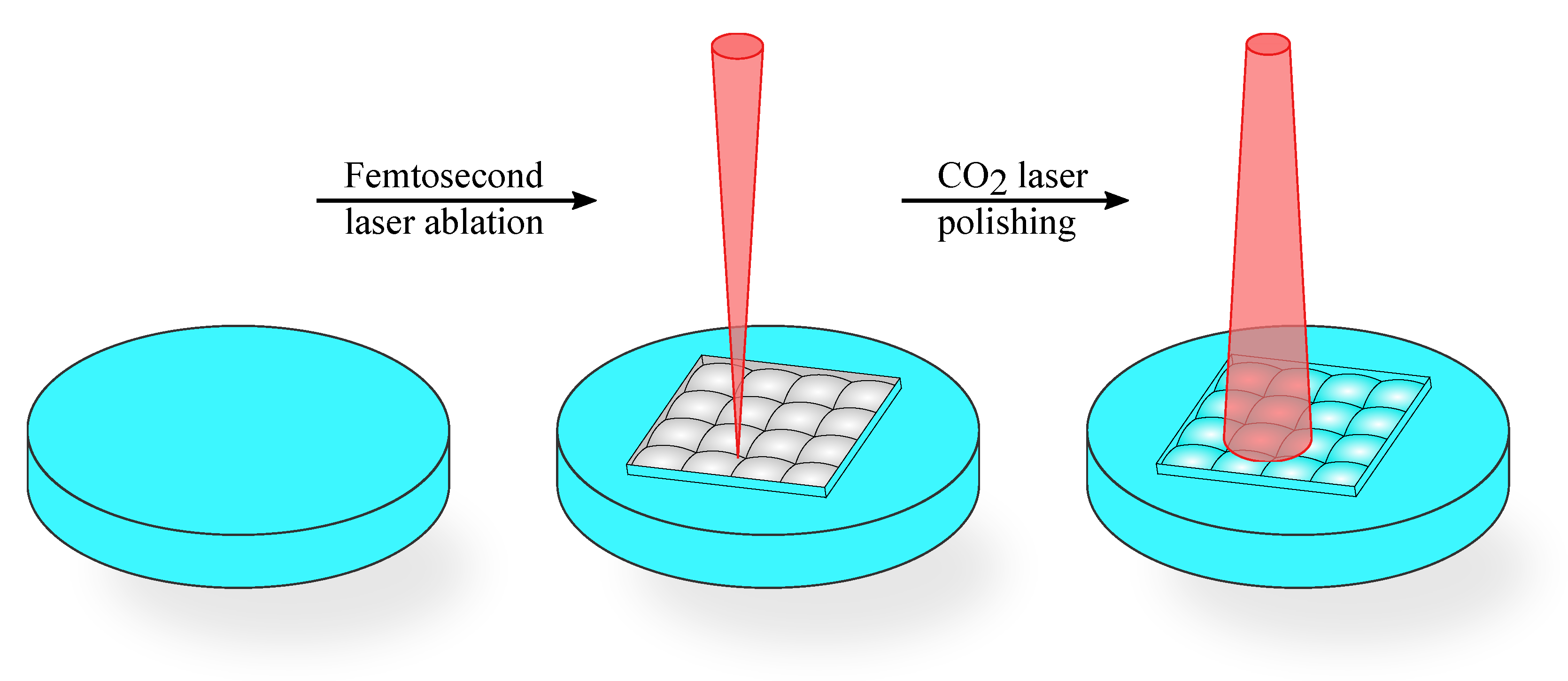
Figure 3.
Evaluation of the fabricated lens array (a) laser-scanning microscope image of the 8 × 8 lens array with magnification and cross-section of a single lens element (b) schematic setup for optical testing of the microlens array with the letter “A”, including a screen, a lensarray and a USB microscope and a section of the captured image.

Figure 4.
Schematic of experimental setup including a halogen light source, a collimator lens (CL), an iris diaphragm/ aperture, the two lens arrays (LA1 & LA2), a Fourier lens (FL) and a camera. The dashed box marks the beam homogenizer used in one housing.
Figure 4.
Schematic of experimental setup including a halogen light source, a collimator lens (CL), an iris diaphragm/ aperture, the two lens arrays (LA1 & LA2), a Fourier lens (FL) and a camera. The dashed box marks the beam homogenizer used in one housing.

Figure 5.
2D, 3D and cross-sectional intensity profiles of the halogen light source (a) after the iris diaphragm and (b) after beam homogenization with the fabricated lens arrays. Note, intensity has been normalized for a better visibility.
Figure 5.
2D, 3D and cross-sectional intensity profiles of the halogen light source (a) after the iris diaphragm and (b) after beam homogenization with the fabricated lens arrays. Note, intensity has been normalized for a better visibility.

Figure 6.
(a) Designed housing (lower part) for beam homogenization with the assembled lens arrays and aperture and (b) schematic of the additive manufacturing process using stereolithography for building the designed object layer by layer out of photosensitive resin.
Figure 6.
(a) Designed housing (lower part) for beam homogenization with the assembled lens arrays and aperture and (b) schematic of the additive manufacturing process using stereolithography for building the designed object layer by layer out of photosensitive resin.
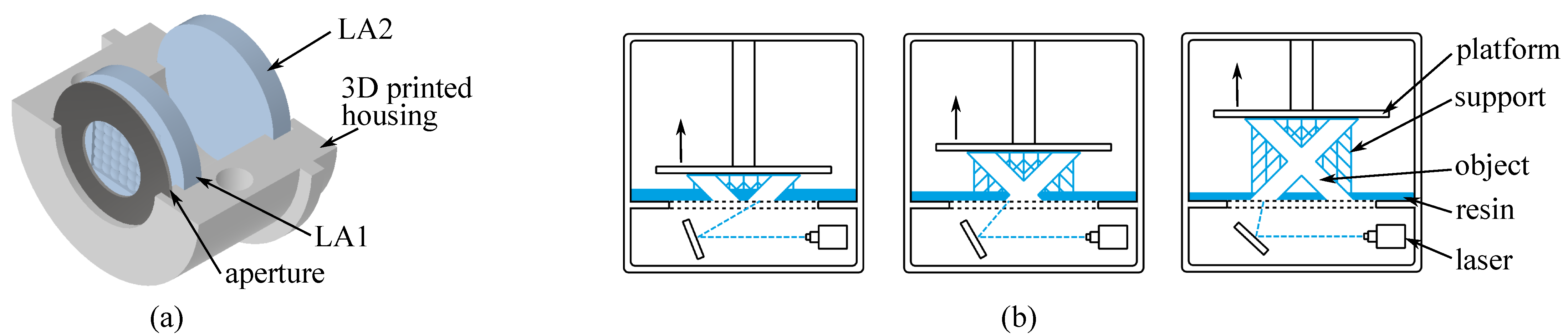
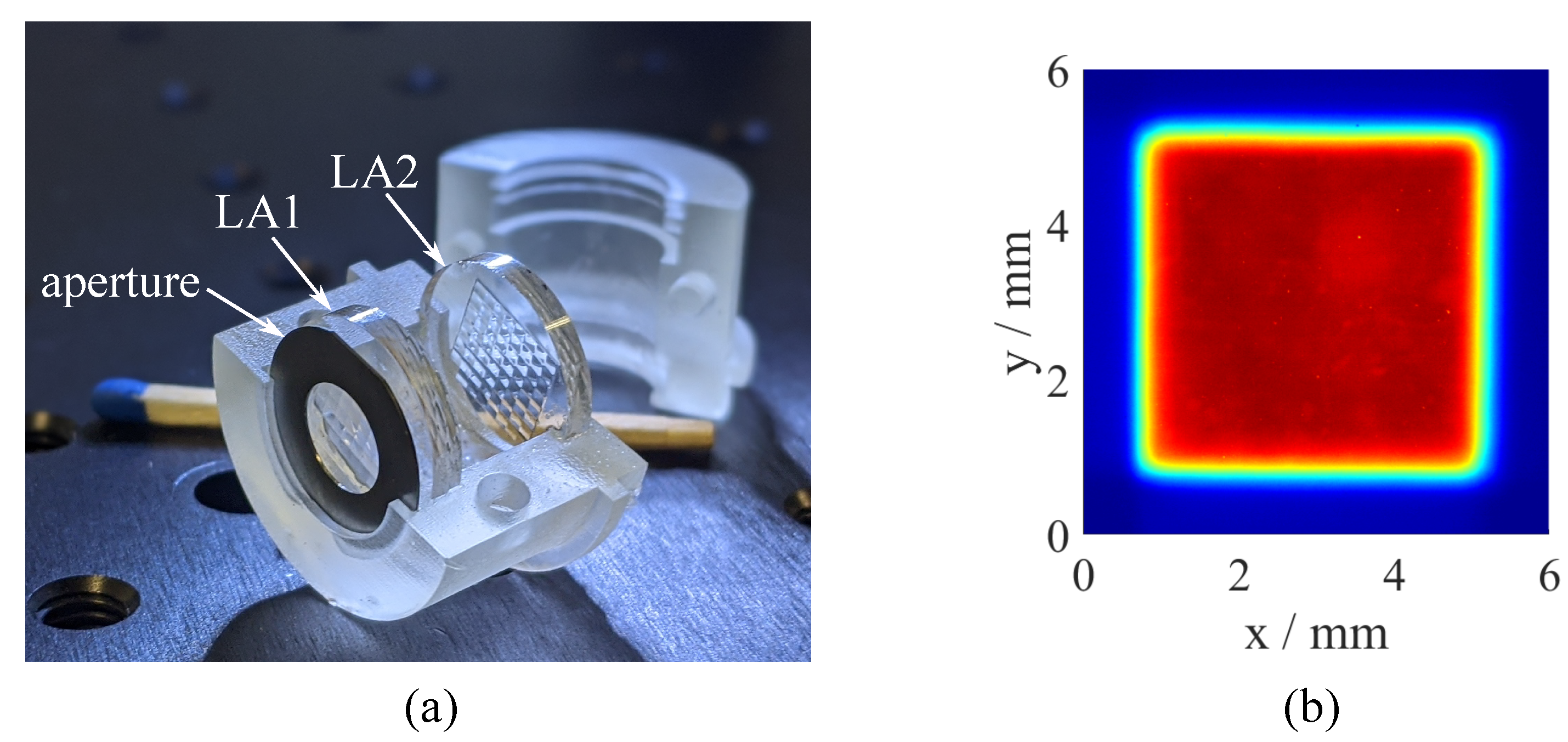
Figure 7.
(a) Final beam shaping module consisting of two lens arrays and an aperture, assembled within a 3D printed housing and (b) Top-Hat beam profile formed by the beam shaping module.
Figure 7.
(a) Final beam shaping module consisting of two lens arrays and an aperture, assembled within a 3D printed housing and (b) Top-Hat beam profile formed by the beam shaping module.

Table 1.
Femtosecond laser based optics fabrication processes.
| Technology | Material | Reference |
|---|---|---|
| Backside wet etching + thermal annealing | Fused silica | Hua et al. [12] |
| Ablation of microholes + wet etching | Silicon | Pan et al. [13] |
| Ablation of microholes + wet etching | Fused silica, sapphire | Zhang et al. [14] |
| Modification of photosensitive glass + thermal treatment, wet etching, annealing | Foturan glass | Lin et al. [15] |
| Ablation (pressure & resoldification) | PDMS | Yong et al. [16] |
| Ablation (pressure & resoldification) | Chalcohalide glass | Kadan et al. [17] |
| Two-photon polymerization | Photoresist | Wu et al. [18] |
| Two-photon polymerization | Photoresist | He et al. [19] |
| Laser ablation + CO laser polishing | Fused silica | Choi et al. [20] |
| Laser ablation + CO laser polishing | Soda-lime glass | Delgado et al. [21] |
Table 2.
Characterization parameters of the generated Top-Hat, calculated by the applied laser camera based on ISO 13694:2000(E) for a threshold of 90%.
Table 2.
Characterization parameters of the generated Top-Hat, calculated by the applied laser camera based on ISO 13694:2000(E) for a threshold of 90%.
| Beam Uniformity | Plateau Uniformity | Flatness Factor | Edge Steepness |
|---|---|---|---|
| 1.8% (ideal 0%) | 2.1% (ideal 0%) | 95.2% (ideal 100%) | 32.8% (ideal 0%) |
Publisher’s Note: MDPI stays neutral with regard to jurisdictional claims in published maps and institutional affiliations. |
© 2021 by the authors. Licensee MDPI, Basel, Switzerland. This article is an open access article distributed under the terms and conditions of the Creative Commons Attribution (CC BY) license (http://creativecommons.org/licenses/by/4.0/).
Share and Cite
MDPI and ACS Style
Schwarz, S.; Götzendorfer, B.; Rung, S.; Esen, C.; Hellmann, R. Compact Beam Homogenizer Module with Laser-Fabricated Lens-Arrays. Appl. Sci. 2021, 11, 1018. https://doi.org/10.3390/app11031018
AMA Style
Schwarz S, Götzendorfer B, Rung S, Esen C, Hellmann R. Compact Beam Homogenizer Module with Laser-Fabricated Lens-Arrays. Applied Sciences. 2021; 11(3):1018. https://doi.org/10.3390/app11031018
Chicago/Turabian StyleSchwarz, Simon, Babette Götzendorfer, Stefan Rung, Cemal Esen, and Ralf Hellmann. 2021. "Compact Beam Homogenizer Module with Laser-Fabricated Lens-Arrays" Applied Sciences 11, no. 3: 1018. https://doi.org/10.3390/app11031018
Note that from the first issue of 2016, this journal uses article numbers instead of page numbers. See further details here.